Fig. 1.
Diagram of a strip of GaAs semi-insulating.
SEMICONDUCTOR DEVICES
A. Resfa, Brahimi.R. Menezla and M. Benchhima
Corresponding author: A. Resfa, Email:rophson@hotmail.com
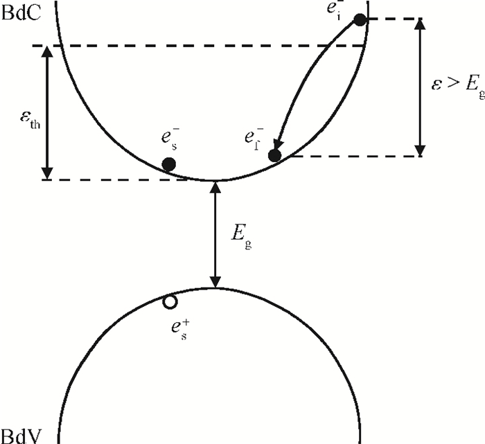
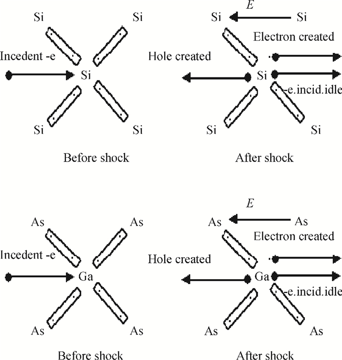
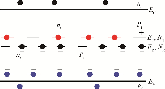
Abstract: This work aims to determine the characteristic I (breakdown voltage) of the inverse current in a GaAs PN junction diode, subject to a reverse polarization, while specifying the parameters that influence the breakdown voltage of the diode. In this work, we simulated the behavior of the ionization phenomenon by impact breakdown by avalanche of the PN junctions, subject to an inverse polarization.We will take into account both the trapping model in a stationary regime in the P+N structure using like material of basis the Ⅲ-Ⅴ compounds and mainly the GaAs semi-insulating in which the deep centers have in important densities. We are talking about the model of trapping in the space charge region (SCR) and that is the trap density donor and acceptor states.The carrier crossing the space charge region (SCR) of W thickness creates N electron-hole pairs:for every created pair, the electron and the hole are swept quickly by the electric field, each in an opposite direction, which comes back, according to an already accepted reasoning, to the crossing of the space charge region (SCR) by an electron or a hole. So the even N pair created by the initial particle provoke N2 ionizations and so forth.The study of the physical and electrical behaviour of semiconductors is based on the influence of the presence of deep centers on the characteristic I(V) current-tension, which requires the calculation of the electrostatic potential, the electric field, the integral of ionization, the density of the states traps, the diffusion current of minority in the regions (1) and (3), the current thermal generation in the region (2), the leakage current in the surface, and the breakdown voltage.
Keywords: the phenomenon of ionization by impact, the integrals of ionizations In and Ip, the potential electrostatic and electric field, variation of the trap state density Nt, the integral of ionization reverse current-breakdown voltage, the current-breakdown voltage characteristics of the P+N junction diode
| [1] |
Mathieu H. Physics of semiconductors and electronic components. Masson Paris, 1996.
|
| [2] |
Kittel C. Physics of the solid state. 7th ed. DUNOD, vol, 7917
|
| [3] |
Brahimi R M, Rahmani N M, Sehil H, et al. Multigridee method for the resolution of coupled system of partiel equations. Conference, Plovdiv, Bulgaria, Aug 13/17, 1995
|
| [4] |
Sze S M. Book of physics of semiconductor devices. 2nd ed. New York:John Wiley, 1981
|
| [5] |
Bonnaud O. PhD Thesis, Central School of Lyon, 1978
|
| [6] |
Mui D S L, Biswas D, Reed J, et al. Investigations of the Si3N4/Si/n-GaAs insulator-semiconductor interface with low interface trap density. Appl Phys Lett, 1992, 60(20):2511 doi: 10.1063/1.106950
|
| [7] |
Pearsall T P. Impact ionization rates for electrons and holes in Ga0.47In0.53As. Appl Phys Lett, 1980, 36(3):218 doi: 10.1063/1.91431
|
| [8] |
Van Overstraeten R, De Man H. Measurement of the ionization rates in diffused silicon PN junction. Solid-State Electron, 1970, 13(5):583 doi: 10.1016/0038-1101(70)90139-5
|
| [9] |
Vapaille et R Castagné A. Semiconductor devices and integrated circuits. Physics and Technology Dunod, 1987 http://www.freepatentsonline.com/9479166.html
|
| [10] |
Boisson V. Study of the optimal geometry the outskirts of planar junction. Thesis, Central School De Lyon, 1985
|
| [11] |
Shockley-Read W. Czech J Phys, 1961, B11(1): 81
|
| [12] |
Grove A S. Physics and technology of semiconductor devices. Dunod-Paris, 1971 https://www.amazon.com/Physics-Technology-Semiconductor-Devices-International/dp/0471329983
|
| [13] |
Fulop W. Solid-State Electron, 1967, 10(1): 39
|
| [14] |
Sze S M, Gibbons G. Avalanche breakdown voltages of abrupt and linearly graded p-n junctions in Ge, Si, GaAs, and GaP. Appl Phys Lett, 1966, 8(5):111 doi: 10.1063/1.1754511
|
| [15] |
Adler M S, Temple V A K. Maximum surface and bulk electric fields at breakdown for planar and beveled devices. IEEE Trans Electron Devices, 1978, 25(10):1266 doi: 10.1109/T-ED.1978.19263
|
| [16] |
Baliga B J, Gandhi J K. Analytical solutions for the breakdown voltage of abrupt cylindrical and spherical junctions. Solid-State Electron, 1976, 19(9):739 doi: 10.1016/0038-1101(76)90152-0
|
| [17] |
Conti F, Conti M. Surface breakdown in silicon planar diodes equipped with field plate. Solid-State Electron, 1972, 15(1):93 doi: 10.1016/0038-1101(72)90070-6
|
| [18] |
Chynoweth A G. Phys Rev, 1950, 109(5): 1537
|
| [19] |
Lee C A, Logan R A, Batdorf R L, et al. Phys Rev, 1964, 134(3A): 761
|
| [20] |
Miller S L. I-MOS:a novel semiconductor device with a subthreshold slope lower than kT/q. Phys Rev, 1955, 99(4):1234 doi: 10.1103/PhysRev.99.1234
|
| [21] |
Taylor D M, Tong D W. The contours of the drilling hole in pulsed laser drilling with inclination angles. Appl Phys, 1984, 56(6):1881 doi: 10.1063/1.334178
|
| [22] |
Urgell J J. Analysis of weak avalanche multiplication in collector junctions:Avalanche injection measurements on standard transistors like devices. Rev Phys Appl (Paris), 1978, 13(12):673 doi: 10.1051/rphysap:019780013012067300
|
| [23] |
Urgell J, Leguerre J R. Experimental determination of the avalanche region of one-sided abrupt barriers. Solid-State Electron, 1974, 17(3):239 doi: 10.1016/0038-1101(74)90011-2
|
| [24] |
Leturcq P. Current-mode analog IC and linearization techniques in CMOS technologies. Thesis, State University of Toulouse, 1976
|
| [25] |
Van Overstraeten R, De Man H. Solid-State Electron, 1970, 13: 583
|
| [26] |
Adler M S, Temple V A K, Rustay R C. Theoretical basis for field calculations on multi-dimensional reverse biased semiconductor devices. Solid-State Electron., 1982, 25(12):1179 doi: 10.1016/0038-1101(82)90077-6
|
| [27] |
Amrani M. Mono-and two-dimensional modeling of CV and Ⅳ characteristics of a PN junction made polycrystalline silicon. Thesis Status Doctor, 1996-2000
|


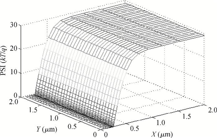
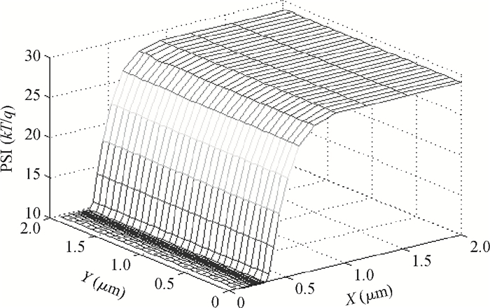
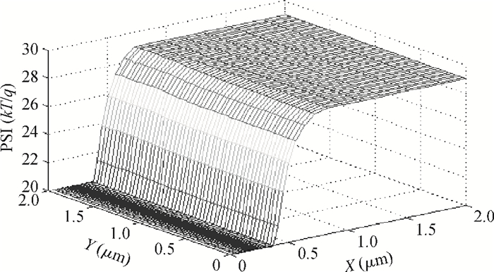
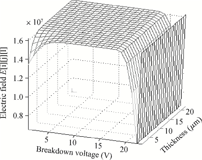


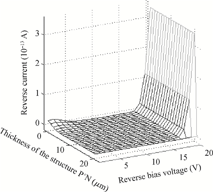
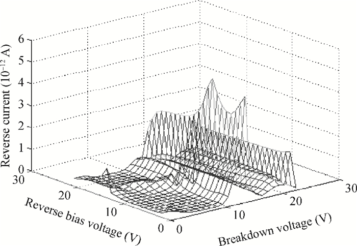
Table 1. The coefficients of ionization.

|
| [1] |
Mathieu H. Physics of semiconductors and electronic components. Masson Paris, 1996.
|
| [2] |
Kittel C. Physics of the solid state. 7th ed. DUNOD, vol, 7917
|
| [3] |
Brahimi R M, Rahmani N M, Sehil H, et al. Multigridee method for the resolution of coupled system of partiel equations. Conference, Plovdiv, Bulgaria, Aug 13/17, 1995
|
| [4] |
Sze S M. Book of physics of semiconductor devices. 2nd ed. New York:John Wiley, 1981
|
| [5] |
Bonnaud O. PhD Thesis, Central School of Lyon, 1978
|
| [6] |
Mui D S L, Biswas D, Reed J, et al. Investigations of the Si3N4/Si/n-GaAs insulator-semiconductor interface with low interface trap density. Appl Phys Lett, 1992, 60(20):2511 doi: 10.1063/1.106950
|
| [7] |
Pearsall T P. Impact ionization rates for electrons and holes in Ga0.47In0.53As. Appl Phys Lett, 1980, 36(3):218 doi: 10.1063/1.91431
|
| [8] |
Van Overstraeten R, De Man H. Measurement of the ionization rates in diffused silicon PN junction. Solid-State Electron, 1970, 13(5):583 doi: 10.1016/0038-1101(70)90139-5
|
| [9] |
Vapaille et R Castagné A. Semiconductor devices and integrated circuits. Physics and Technology Dunod, 1987 http://www.freepatentsonline.com/9479166.html
|
| [10] |
Boisson V. Study of the optimal geometry the outskirts of planar junction. Thesis, Central School De Lyon, 1985
|
| [11] |
Shockley-Read W. Czech J Phys, 1961, B11(1): 81
|
| [12] |
Grove A S. Physics and technology of semiconductor devices. Dunod-Paris, 1971 https://www.amazon.com/Physics-Technology-Semiconductor-Devices-International/dp/0471329983
|
| [13] |
Fulop W. Solid-State Electron, 1967, 10(1): 39
|
| [14] |
Sze S M, Gibbons G. Avalanche breakdown voltages of abrupt and linearly graded p-n junctions in Ge, Si, GaAs, and GaP. Appl Phys Lett, 1966, 8(5):111 doi: 10.1063/1.1754511
|
| [15] |
Adler M S, Temple V A K. Maximum surface and bulk electric fields at breakdown for planar and beveled devices. IEEE Trans Electron Devices, 1978, 25(10):1266 doi: 10.1109/T-ED.1978.19263
|
| [16] |
Baliga B J, Gandhi J K. Analytical solutions for the breakdown voltage of abrupt cylindrical and spherical junctions. Solid-State Electron, 1976, 19(9):739 doi: 10.1016/0038-1101(76)90152-0
|
| [17] |
Conti F, Conti M. Surface breakdown in silicon planar diodes equipped with field plate. Solid-State Electron, 1972, 15(1):93 doi: 10.1016/0038-1101(72)90070-6
|
| [18] |
Chynoweth A G. Phys Rev, 1950, 109(5): 1537
|
| [19] |
Lee C A, Logan R A, Batdorf R L, et al. Phys Rev, 1964, 134(3A): 761
|
| [20] |
Miller S L. I-MOS:a novel semiconductor device with a subthreshold slope lower than kT/q. Phys Rev, 1955, 99(4):1234 doi: 10.1103/PhysRev.99.1234
|
| [21] |
Taylor D M, Tong D W. The contours of the drilling hole in pulsed laser drilling with inclination angles. Appl Phys, 1984, 56(6):1881 doi: 10.1063/1.334178
|
| [22] |
Urgell J J. Analysis of weak avalanche multiplication in collector junctions:Avalanche injection measurements on standard transistors like devices. Rev Phys Appl (Paris), 1978, 13(12):673 doi: 10.1051/rphysap:019780013012067300
|
| [23] |
Urgell J, Leguerre J R. Experimental determination of the avalanche region of one-sided abrupt barriers. Solid-State Electron, 1974, 17(3):239 doi: 10.1016/0038-1101(74)90011-2
|
| [24] |
Leturcq P. Current-mode analog IC and linearization techniques in CMOS technologies. Thesis, State University of Toulouse, 1976
|
| [25] |
Van Overstraeten R, De Man H. Solid-State Electron, 1970, 13: 583
|
| [26] |
Adler M S, Temple V A K, Rustay R C. Theoretical basis for field calculations on multi-dimensional reverse biased semiconductor devices. Solid-State Electron., 1982, 25(12):1179 doi: 10.1016/0038-1101(82)90077-6
|
| [27] |
Amrani M. Mono-and two-dimensional modeling of CV and Ⅳ characteristics of a PN junction made polycrystalline silicon. Thesis Status Doctor, 1996-2000
|


Article views: 3793 Times PDF downloads: 38 Times Cited by: 0 Times
Received: 27 December 2013 Revised: 15 February 2014 Online: Published: 01 August 2014
| Citation: |
A. Resfa, Brahimi.R. Menezla, M. Benchhima. Simulating and modeling the breakdown voltage in a semi-insulating GaAs P+N junction diode[J]. Journal of Semiconductors, 2014, 35(8): 084002. doi: 10.1088/1674-4926/35/8/084002
****
A. Resfa, B. R. Menezla, M. Benchhima. Simulating and modeling the breakdown voltage in a semi-insulating GaAs P+N junction diode[J]. J. Semicond., 2014, 35(8): 084002. doi: 10.1088/1674-4926/35/8/084002.

|
| [1] |
Mathieu H. Physics of semiconductors and electronic components. Masson Paris, 1996.
|
| [2] |
Kittel C. Physics of the solid state. 7th ed. DUNOD, vol, 7917
|
| [3] |
Brahimi R M, Rahmani N M, Sehil H, et al. Multigridee method for the resolution of coupled system of partiel equations. Conference, Plovdiv, Bulgaria, Aug 13/17, 1995
|
| [4] |
Sze S M. Book of physics of semiconductor devices. 2nd ed. New York:John Wiley, 1981
|
| [5] |
Bonnaud O. PhD Thesis, Central School of Lyon, 1978
|
| [6] |
Mui D S L, Biswas D, Reed J, et al. Investigations of the Si3N4/Si/n-GaAs insulator-semiconductor interface with low interface trap density. Appl Phys Lett, 1992, 60(20):2511 doi: 10.1063/1.106950
|
| [7] |
Pearsall T P. Impact ionization rates for electrons and holes in Ga0.47In0.53As. Appl Phys Lett, 1980, 36(3):218 doi: 10.1063/1.91431
|
| [8] |
Van Overstraeten R, De Man H. Measurement of the ionization rates in diffused silicon PN junction. Solid-State Electron, 1970, 13(5):583 doi: 10.1016/0038-1101(70)90139-5
|
| [9] |
Vapaille et R Castagné A. Semiconductor devices and integrated circuits. Physics and Technology Dunod, 1987 http://www.freepatentsonline.com/9479166.html
|
| [10] |
Boisson V. Study of the optimal geometry the outskirts of planar junction. Thesis, Central School De Lyon, 1985
|
| [11] |
Shockley-Read W. Czech J Phys, 1961, B11(1): 81
|
| [12] |
Grove A S. Physics and technology of semiconductor devices. Dunod-Paris, 1971 https://www.amazon.com/Physics-Technology-Semiconductor-Devices-International/dp/0471329983
|
| [13] |
Fulop W. Solid-State Electron, 1967, 10(1): 39
|
| [14] |
Sze S M, Gibbons G. Avalanche breakdown voltages of abrupt and linearly graded p-n junctions in Ge, Si, GaAs, and GaP. Appl Phys Lett, 1966, 8(5):111 doi: 10.1063/1.1754511
|
| [15] |
Adler M S, Temple V A K. Maximum surface and bulk electric fields at breakdown for planar and beveled devices. IEEE Trans Electron Devices, 1978, 25(10):1266 doi: 10.1109/T-ED.1978.19263
|
| [16] |
Baliga B J, Gandhi J K. Analytical solutions for the breakdown voltage of abrupt cylindrical and spherical junctions. Solid-State Electron, 1976, 19(9):739 doi: 10.1016/0038-1101(76)90152-0
|
| [17] |
Conti F, Conti M. Surface breakdown in silicon planar diodes equipped with field plate. Solid-State Electron, 1972, 15(1):93 doi: 10.1016/0038-1101(72)90070-6
|
| [18] |
Chynoweth A G. Phys Rev, 1950, 109(5): 1537
|
| [19] |
Lee C A, Logan R A, Batdorf R L, et al. Phys Rev, 1964, 134(3A): 761
|
| [20] |
Miller S L. I-MOS:a novel semiconductor device with a subthreshold slope lower than kT/q. Phys Rev, 1955, 99(4):1234 doi: 10.1103/PhysRev.99.1234
|
| [21] |
Taylor D M, Tong D W. The contours of the drilling hole in pulsed laser drilling with inclination angles. Appl Phys, 1984, 56(6):1881 doi: 10.1063/1.334178
|
| [22] |
Urgell J J. Analysis of weak avalanche multiplication in collector junctions:Avalanche injection measurements on standard transistors like devices. Rev Phys Appl (Paris), 1978, 13(12):673 doi: 10.1051/rphysap:019780013012067300
|
| [23] |
Urgell J, Leguerre J R. Experimental determination of the avalanche region of one-sided abrupt barriers. Solid-State Electron, 1974, 17(3):239 doi: 10.1016/0038-1101(74)90011-2
|
| [24] |
Leturcq P. Current-mode analog IC and linearization techniques in CMOS technologies. Thesis, State University of Toulouse, 1976
|
| [25] |
Van Overstraeten R, De Man H. Solid-State Electron, 1970, 13: 583
|
| [26] |
Adler M S, Temple V A K, Rustay R C. Theoretical basis for field calculations on multi-dimensional reverse biased semiconductor devices. Solid-State Electron., 1982, 25(12):1179 doi: 10.1016/0038-1101(82)90077-6
|
| [27] |
Amrani M. Mono-and two-dimensional modeling of CV and Ⅳ characteristics of a PN junction made polycrystalline silicon. Thesis Status Doctor, 1996-2000
|

 WeChat ID
Journal of Semiconductors © 2017 All Rights Reserved 京ICP备05085259号-2

 DownLoad: