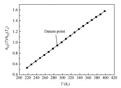
Fig. 1.
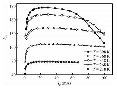
The $h_{\rm FE}$ -$I_{\rm C}$ curve at different temperatures
SEMICONDUCTOR DEVICES
Haochun Qi1, 2, , Xiaoling Zhang1, Xuesong Xie1, Li Zhao1, Chengju Chen1 and Changzhi Lü1
Corresponding author: Qi Haochun, Email:jetqi@sina.com
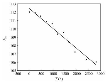
Abstract: Considering the impacts of ideal factor n, VBE and band gap changes with the temperature on current gain, the current gain expression has been corrected to make the results closer to the actual test. Besides, the accelerating lifetime study method in the constant temperature-humidity stress is used to estimate the reliability of the same batch transistors. Applying the revised findings from the expression, the current gains before and after the test are compared and analyzed, and, according to the degradation data of the current gain, the transistor lifetimes in the test stress are respectively extrapolated in the different failure criteria.
Keywords: bipolar transistors, temperature feature, current gain, accelerating lifetime
| [1] |
Li Xuexin, Lin Yayun. Investigation of current-gain temperature dependence in bipolar transistors. Acta Electronica Sinica, 1984, 5:45
|
| [2] |
Li Zhiguo, Cheng Yaohai, Sun Yinghua, et al. The analysis of bipolar transistor hFE failure under low temperature and its reliability in application. Journal of Beijing Polytechnic University, 1996, 4:25
|
| [3] |
He Jian, Xu Xueliang. Study on temperature effects on current gain of bipolar transistor. J Microelectron, 2012, 2:270
|
| [4] |
Zheng J, Wu J, Wei T. Silicon bipolar transistors with temperature stable current gain. J Electron Devices, 1991, 1:44
|
| [5] |
Gao Guangbo, Li Xuexing. Semiconductor device reliability physics. Science Press, 1987:71
|
| [6] |
Pierret R F. Semiconductor device fundamentals. 2nd ed. Addison Wesley, 1996
|
| [7] |
Vol'fson A A, Suvashiev V K. Fundamental absorption edge of silicon heavily doped with donor or acceptor impurities. Sov Physics Semiconductors, 1961, 1:327
|
| [8] |
He M, Li H F, Wang P I, et al. Bias temperature stress of Al on porous low-k dielectric. Microelectron Reliab, 2011, 51(8):1342 doi: 10.1016/j.microrel.2011.03.004
|
| [9] |
Qi Haochun, Lü Changzhi, Zhang Xiaoling, et al. Accelerating the life of transistors. Journal of Semiconductors, 2013, 34(6):064010 doi: 10.1088/1674-4926/34/6/064010
|
| [10] |
Zhao L, Tokei Z, Croes K, et al. Direct observation of the 1/E dependence of time dependent dielectric breakdown in the presence of copper. Appl Phys Lett, 2011, 98:032107 doi: 10.1063/1.3543850
|
| [11] |
Lloyda J R, Liniger E, Shaw T M. Simple model for time-dependent dielectric breakdown in inter-and intralevel low-k dielectrics. J Appl Phys, 2005, 98:084109 doi: 10.1063/1.2112171
|
| [12] |
Chen F, Bravo B, Chanda K, et al. A comprehensive study of low-k SiCOH TDDB phenomena and its reliability lifetime model development. Proceedings of International Reliability Physics Symposium, 2006:46
|
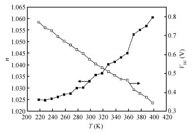
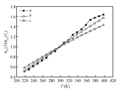
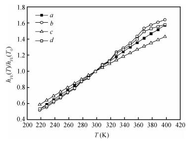
Table 1.

|
Table 2.

|
Table 3. Extrapolated lifetimes of test samples at three groups

|
Table 4. Parameter assessment in three common distributions

|
| [1] |
Li Xuexin, Lin Yayun. Investigation of current-gain temperature dependence in bipolar transistors. Acta Electronica Sinica, 1984, 5:45
|
| [2] |
Li Zhiguo, Cheng Yaohai, Sun Yinghua, et al. The analysis of bipolar transistor hFE failure under low temperature and its reliability in application. Journal of Beijing Polytechnic University, 1996, 4:25
|
| [3] |
He Jian, Xu Xueliang. Study on temperature effects on current gain of bipolar transistor. J Microelectron, 2012, 2:270
|
| [4] |
Zheng J, Wu J, Wei T. Silicon bipolar transistors with temperature stable current gain. J Electron Devices, 1991, 1:44
|
| [5] |
Gao Guangbo, Li Xuexing. Semiconductor device reliability physics. Science Press, 1987:71
|
| [6] |
Pierret R F. Semiconductor device fundamentals. 2nd ed. Addison Wesley, 1996
|
| [7] |
Vol'fson A A, Suvashiev V K. Fundamental absorption edge of silicon heavily doped with donor or acceptor impurities. Sov Physics Semiconductors, 1961, 1:327
|
| [8] |
He M, Li H F, Wang P I, et al. Bias temperature stress of Al on porous low-k dielectric. Microelectron Reliab, 2011, 51(8):1342 doi: 10.1016/j.microrel.2011.03.004
|
| [9] |
Qi Haochun, Lü Changzhi, Zhang Xiaoling, et al. Accelerating the life of transistors. Journal of Semiconductors, 2013, 34(6):064010 doi: 10.1088/1674-4926/34/6/064010
|
| [10] |
Zhao L, Tokei Z, Croes K, et al. Direct observation of the 1/E dependence of time dependent dielectric breakdown in the presence of copper. Appl Phys Lett, 2011, 98:032107 doi: 10.1063/1.3543850
|
| [11] |
Lloyda J R, Liniger E, Shaw T M. Simple model for time-dependent dielectric breakdown in inter-and intralevel low-k dielectrics. J Appl Phys, 2005, 98:084109 doi: 10.1063/1.2112171
|
| [12] |
Chen F, Bravo B, Chanda K, et al. A comprehensive study of low-k SiCOH TDDB phenomena and its reliability lifetime model development. Proceedings of International Reliability Physics Symposium, 2006:46
|


Article views: 2999 Times PDF downloads: 12 Times Cited by: 0 Times
Received: 09 January 2014 Revised: 13 March 2014 Online: Published: 01 September 2014
| Citation: |
Haochun Qi, Xiaoling Zhang, Xuesong Xie, Li Zhao, Chengju Chen, Changzhi Lü. The expression correction of transistor current gain and its application in reliability assessment[J]. Journal of Semiconductors, 2014, 35(9): 094008. doi: 10.1088/1674-4926/35/9/094008
****
H C Qi, X L Zhang, X S Xie, L Zhao, C J Chen, C Z Lü. The expression correction of transistor current gain and its application in reliability assessment[J]. J. Semicond., 2014, 35(9): 094008. doi: 10.1088/1674-4926/35/9/094008.

|
| [1] |
Li Xuexin, Lin Yayun. Investigation of current-gain temperature dependence in bipolar transistors. Acta Electronica Sinica, 1984, 5:45
|
| [2] |
Li Zhiguo, Cheng Yaohai, Sun Yinghua, et al. The analysis of bipolar transistor hFE failure under low temperature and its reliability in application. Journal of Beijing Polytechnic University, 1996, 4:25
|
| [3] |
He Jian, Xu Xueliang. Study on temperature effects on current gain of bipolar transistor. J Microelectron, 2012, 2:270
|
| [4] |
Zheng J, Wu J, Wei T. Silicon bipolar transistors with temperature stable current gain. J Electron Devices, 1991, 1:44
|
| [5] |
Gao Guangbo, Li Xuexing. Semiconductor device reliability physics. Science Press, 1987:71
|
| [6] |
Pierret R F. Semiconductor device fundamentals. 2nd ed. Addison Wesley, 1996
|
| [7] |
Vol'fson A A, Suvashiev V K. Fundamental absorption edge of silicon heavily doped with donor or acceptor impurities. Sov Physics Semiconductors, 1961, 1:327
|
| [8] |
He M, Li H F, Wang P I, et al. Bias temperature stress of Al on porous low-k dielectric. Microelectron Reliab, 2011, 51(8):1342 doi: 10.1016/j.microrel.2011.03.004
|
| [9] |
Qi Haochun, Lü Changzhi, Zhang Xiaoling, et al. Accelerating the life of transistors. Journal of Semiconductors, 2013, 34(6):064010 doi: 10.1088/1674-4926/34/6/064010
|
| [10] |
Zhao L, Tokei Z, Croes K, et al. Direct observation of the 1/E dependence of time dependent dielectric breakdown in the presence of copper. Appl Phys Lett, 2011, 98:032107 doi: 10.1063/1.3543850
|
| [11] |
Lloyda J R, Liniger E, Shaw T M. Simple model for time-dependent dielectric breakdown in inter-and intralevel low-k dielectrics. J Appl Phys, 2005, 98:084109 doi: 10.1063/1.2112171
|
| [12] |
Chen F, Bravo B, Chanda K, et al. A comprehensive study of low-k SiCOH TDDB phenomena and its reliability lifetime model development. Proceedings of International Reliability Physics Symposium, 2006:46
|

 WeChat ID
Journal of Semiconductors © 2017 All Rights Reserved 京ICP备05085259号-2

 DownLoad: