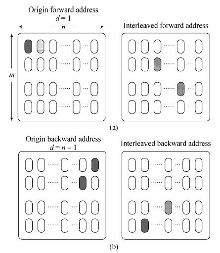
Loading [MathJax]/jax/output/HTML-CSS/jax.js
J. Semicond. > 2015, Volume 36 > Issue 7 > 075003

SEMICONDUCTOR INTEGRATED CIRCUITS

LTE turbo decoder design

Le Yang, Tianchun Ye, Bin Wu and Ruiqi Zhang

+ Author Affiliations

 Corresponding author: Bin Wu, E-mail: wubin@ime.ac.cn

DOI: 10.1088/1674-4926/36/7/075003

PDF

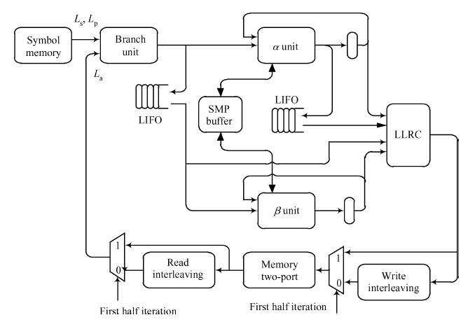
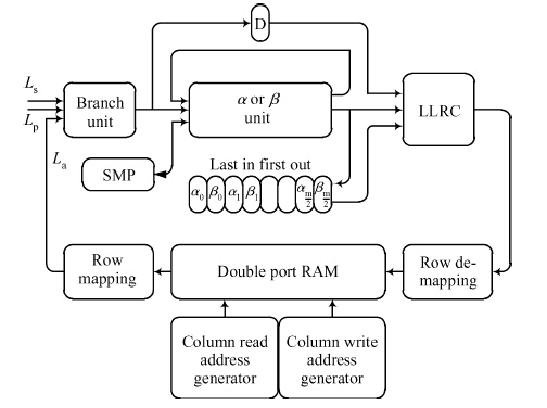
Abstract: This paper presents a turbo decoder supporting all 188 block sizes in 3GPP long term evolution (LTE) standard which can be employed in the LTE micro-eNodB system. The design allows 1, 2, 4, 8 or 16 soft-in/soft-out (SISO) decoders to concurrently process each block size, and the number of iterations can be adjusted. This article proposes an improved SISO algorithm and interleaving design, calculated forward state matrix and backward state matrix alternately, and the branch transition probability can be used in the Turbo decode process directly just after one clock delay. The structure enables a decoder processing radix-2 algorithm with high speed, instead of radix-4 as the conventional decoder. Moreover, the paper details an interleaver/de-interleaver, which is combined by two operational steps. One is column address mapping and the other is intra-row permutation. Decoder realizes interleaving by loading data from memories whose address is generated by column mapping and then lets data passing through inter-row permutation. For de-interleaving, the system can adopt reverse operation.

Key words: LTEturbo decoder(quadratic polynomial permutation) QPP interleaver

3GPP LTE, which is a set of enhancements to the 3G Universal Mobile Telecommunications System (UMTS)[1], has received tremendous attention recently and is considered to be a very promising 4G wireless technology. The Turbo decoder is typically one of the major blocks in a LTE wireless receiver. Key requirements of LTE include packet data support with peak data rates up to 150 Mbps on the downlink and 75 Mbps on the uplink, a low latency of 10 ms layer-2 round trip delay, flexible bandwidths (up to 20 MHz), improved system capacity and coverage[2]. Advanced technologies were selected to meet these requirements including the turbo decoder.

The bottleneck of turbo decoder design is the high latency which is due to the iterative decoding process, the forward-backward recursion in the maximum a posteriori (MAP) decoding algorithm and the interleaving/de-interleaving between iterations. In this brief, the codeword can be processed concurrently by four, eight or sixteen SISO decoders. The design challenge for these parallel modes is how to transmit parallel data simultaneously through the interconnection between SISO decoders and the memory module[3].

To achieve high throughput decoder, the low-latency of SISO and interleaver/de-interleaver had to be considered. This brief focuses on these issues and proposes an improved architecture. For a novel SISO system, forward state matrix α and backward state matrix β are calculated alternately, where the design made both algorithms share the same structure and had less crucial path delay. The improved interleaver/de-interleaver structure realized interleaving and de-interleaving in one cycle.

The rest of the sections in this paper are organized as follows. Section 2 describes the basic structure of QPP and its several algebraic properties. Then this article proposes an interleaver/de-interleaver design based on QPP algebraic properties. Section 3 concentrates on novel SISO architecture, which uses less resources and has low-latency for the Log{\_}map algorithm. Section 4 provides the implementation results followed by a conclusion.

The interleaver is essential to the impressive performance of the Turbo code, but its pseudorandom property complicates the parallel processing of a single codeword. A specific mechanism is required to handle parallel data transmission with traditional interleavers[4].

The QPP interleaver of a size-N block can be expressed as

f(x)=f1x+f2x2modN,(1)
The x stands for the original address and the f(x) is the interleaved address. The determination of f1 and f2 is related to the block size. In LTE standard specification, f1 is always defined as an odd number while f2 is even. Moreover LTE, the block size N is always divisible by 16, 32, and 64 when N 512, 1024, and 2048, respectively. This formula requires intensive calculation as it uses a square, a multiply and reminder operation. An approach to reduce operations is to consider the calculations are done in a progressive way. The reminder of the operations are done in every calculation cycle, then it can be reduced simply. The square and multiply would not be needed anymore. The QPP interleaver can transfer as follows.
f(x+d)=[f(x)+g(x)]modN,(2)
g(x)=(2df2x+d2f2+f1d)modN,(3)
g(x+d)=[g(x)+2d2f2]modN,(4)
where g(x) is middle stage and d is interleaver step. In this article, decode data would divide into several groups, while all groups can be processed at the same time[5].

As Figure 1 shows, decode data is saved in m×n matrix, where m indicates the number of groups and n stands for each group length. Two steps are exploited in parallel interleaving design. Step d is equal to 1 for the forward interleaver while for the backward one, d would be n1. Figure 1(a) shows the forward interleaver. Successive two sequences after the interleaver are mapped in different line and row. Figure 1(b) illustrates the backward interleaving process. In backward interleaver sequences, two original adjacent numbers lie with both neighbor in column and line. After backward interleaving, they are separated in a different line and column. The setting means the two interleavers can be uniform disposal.

Figure  1.  Matrix interleaving.

However, we can deduce some properties from QPP interleaver formula which is very useful for interleaving processing. QPP equator can be rewritten as follows.

f(x)=f1(x+w)+f2(x+w)2modn=f1x+f2x2modn,(5)
where w can be divided by n. From Equation (5), we can draw a conclusion that parallel data can be read at the same address from different memories.

Figure 2 shows that process. The column interleaving generator combines by two progressive adders. Forward column address generator equations, for computing forward state matrix α, shown as follows.

f(x+1)=[f(x)+G(x)]modn,(6)
f(x+1)=[f(x)+G(x)]modn,(7)
G(x+1)=[G(x)+delta]modn,(8)
delta=(2f2)modn,(9)
G(0)=(f1+f2)modn,(10)
f(0)=0,(11)
where x ranged from 0 to n - 1, is the forward sequence. f(x) is the forward interleaved column address. The same as the forward address generator, backward address generator equations can be expressed as follows:

f(x1)=[f(x)+G(x)]modn,

(12)

G(x1)=[G(x)+delta]modn,

(13)

delta=(2f2)modn,

(14)

G(n1)=(3f2f1)modn,

(15)

f(n1)=(f2f1)modn.

(16)

In these group formulas, x is the backward sequence, covered from n - 1 to 0. f(x1) is the backward interleaved column address. The signal column{\_}c{\_}in would be used in an intra-row permutation process.

Figure 2 illustrates only half of the interleaver/de-interleaver operation and intra-row permutation is another half. Figure 3 gives more detail.

Figure  2.  Column mapping address generator.
Figure  3.  Intra-row permutation generator.

Intra-row permutation includes 16-groups progressive adders. Figure 3 illustrates one group work. Equations (17)-(19) show intra-row permutation. Where m is the number of groups covered 1, 4, 8 or 16, so we can just keep 2, 3 or 4 bits corresponding to the final result instead of the reminder operation.

f(x+1)={[f(x)+g(x)]%n}modm,

(17)

g(x+1)={[g(x)+delta]%n}modm,

(18)

delta=[(2f2)%n]modm.

(19)

For forward address calculation, the equator can be transformed to

row_f(w+x+1)=(row_f(w+x)+row_g(x))modm,

(20)

row_g(w+x+1)=(row_g(w+x)+row_delta)modm,

(21)

row_delta=((2f2)%n+column_c_in)modm,

(22)

row_g(0)=[g(0)%n]modm,

(23)

row_f(0)=[f(0)%n]modm.

(24)

The same as the forward intra-row permutation, backward calculation can use the same architecture with different initial inputs. Two permutations can share the same adders in various time slots. However, backward intra-row permutation should be adjusted, because the next permutation is in the following line. By this way, the Turbo decoder can generate a mapping/demapping address every cycle.

row_f(w+x1)=(row_f(w+x)+row_g(w+x))modm,

(25)

row_g(w+x1)=(row_g(w+x)+row_delta)modm,

(26)

row_delta=((2f2)%n+column_c_in)modm,

(27)

row_g(n1)=[g(n1)%n]modm,

(28)

row_f(n1)=[f(n1)%n]modm.

(29)

In order to illustrate the improved MAP shown in Figure 5, we compare it with original sliding window MAP (SW-MAP). Figure 4 shows common SW-MAP decoder architecture which requires one set of α unit, β unit, branch unit, and a Log Likelihood Ratio Calculator (LLRC) unit. A SMP buffer is used to save the stakes for use in the next Turbo iteration. In the SW algorithm, the parity Lp is loaded from the symbol memory in the sequential order. Priori information La is loaded from the double port memory in the sequential order for the first half iteration, and in the interleaving order for the second half iteration[6]. The same as the La information loading scheme, the systematic Ls is the load from the symbol memory. However, the ordinary SW-MAP design has two problems. One is α and β calculation which employs fully parallel add-compare-select-add[7]. This operation needs to be completed in one cycle which means the decoder cannot work in the high speed clock system. Another problem is resource consumption. The new design scopes on these two issues and employs mending structure.

Figure  4.  SW-MAP decoder architecture.
Figure  5.  Improved SISO decoder.

The new add-compare-select-add operator idea is separated into two parts by a register. Two parts can deal different operation, one calculated α while the other calculated β or vice versa. Both α unit and β unit can be replaced by α or β unit. In this way, two α or β units can finish all α and β computation with one clock more than conversion SISO but shorten the critical path delay. Since the output sequence is different, the construction has to be taken.

Compared with a conventional SW-MAP decoder, the improved decoder does not use a sliding window and has only one α or β unit instead of α unit and β unit in the old one. Because α and β calculator structures are almost the same except branch transition probability mapping which can be control by mode select. What is more, the branch of last in first out memory (LIFO) had been saved because it takes parts in LLRC calculation directly.

In the improved MAP decoder, α and β are calculated alternately. Both α unit and β unit employ an add-compare-select-add operator, which is decided critical path delay in IC design ascertaining the system clock. To solve this bottleneck, a register is utilized to split the operator into add-compare and select-add. Because state matrix α and backward state β are independent of each other, the α or β unit calculates α and β in turn. The novel scheme not only yields a fast system clock but also reduces resource consumption by reusing the unit. Alternatively calculating α and β has another advantage: the transition probability computed by the branch unit need not save at all, which takes part in LLRC decoding directly with a clock delay. The new design finished half an iteration in the double group length clock, while SW-MAP using a group length and the width of the window. In short, two new MAP decoders are equivalent~to one SW-MAP decoder in complex, and spend less time in decoding.

Table 1 summarizes the implementation result of the proposed decoder and the hardware comparison with existing decoders. The new SISO architecture was only a trial by FPGA and would be verified by a trial chip in the future.

Table  1.  Key characteristics comparison with published turbo decoders.
DownLoad: CSV  | Show Table

This paper details the implementation of a parallel Turbo decoder for the LTE standard, analyzing aspects including interleaving and SISO design, and the verification idea in FPGA. The proposed circuit is designed to achieve high throughput. Interleaver and Log-MAP algorithm optimizations in a parallelized architecture make it possible to achieve high throughput rates with low latency, without performance loss.


[1]
[2]
[3]
[4]
[5]
[6]
[7]
[8]
[9]
Fig. 1.  Matrix interleaving.

Fig. 2.  Column mapping address generator.

Fig. 3.  Intra-row permutation generator.

Fig. 4.  SW-MAP decoder architecture.

Fig. 5.  Improved SISO decoder.

DownLoad: CSV
DownLoad: CSV
DownLoad: CSV
DownLoad: CSV
DownLoad: CSV
DownLoad: CSV
DownLoad: CSV
DownLoad: CSV
DownLoad: CSV
DownLoad: CSV
DownLoad: CSV

Table 1.   Key characteristics comparison with published turbo decoders.

DownLoad: CSV
[1]
[2]
[3]
[4]
[5]
[6]
[7]
[8]
[9]
1

Magnetic LEGO: van der Vaals interlayer magnetism

Lifeng Yin

Journal of Semiconductors, 2019, 40(12): 120201. doi: 10.1088/1674-4926/40/12/120201

2

Dual material gate doping-less tunnel FET with hetero gate dielectric for enhancement of analog/RF performance

Sunny Anand, R.K. Sarin

Journal of Semiconductors, 2017, 38(2): 024001. doi: 10.1088/1674-4926/38/2/024001

3

Effect of band gap energy on the electrical conductivity in doped ZnO thin film

Said Benramache, Okba Belahssen, Hachemi Ben Temam

Journal of Semiconductors, 2014, 35(7): 073001. doi: 10.1088/1674-4926/35/7/073001

4

Structural, morphological, dielectrical and magnetic properties of Mn substituted cobalt ferrite

S. P. Yadav, S. S. Shinde, A. A. Kadam, K. Y. Rajpure

Journal of Semiconductors, 2013, 34(9): 093002. doi: 10.1088/1674-4926/34/9/093002

5

A saw-less direct conversion long term evolution receiver with 25% duty-cycle LO in 130 nm CMOS technology

Siyuan He, Changhong Zhang, Liang Tao, Weifeng Zhang, Longyue Zeng, et al.

Journal of Semiconductors, 2013, 34(3): 035002. doi: 10.1088/1674-4926/34/3/035002

6

Structural parameters improvement of an integrated HBT in a cascode configuration opto-electronic mixer

Hassan Kaatuzian, Hadi Dehghan Nayeri, Masoud Ataei, Ashkan Zandi

Journal of Semiconductors, 2013, 34(9): 094001. doi: 10.1088/1674-4926/34/9/094001

7

A high linearity downconverter for SAW-less LTE receivers

Jiang Peichen, Guan Rui, Wang Wufeng, Chen Dongpo, Zhou Jianjun, et al.

Journal of Semiconductors, 2012, 33(10): 105002. doi: 10.1088/1674-4926/33/10/105002

8

A multi-mode multi-band RF receiver front-end for a TD-SCDMA/LTE/LTE-advanced in 0.18-μm CMOS process

Guo Rui, Zhang Haiying

Journal of Semiconductors, 2012, 33(9): 095003. doi: 10.1088/1674-4926/33/9/095003

9

A 6th order wideband active-RC LPF for LTE application

Wei Baoyue, Li Hongkun, Wang Yunfeng, Zhang Haiying

Journal of Semiconductors, 2012, 33(6): 065003. doi: 10.1088/1674-4926/33/6/065003

10

A wide-band low phase noise LC-tuned VCO with constant KVCOosc for LTE PLL

Huang Jiwei, Wang Zhigong, Li Kuili, Li Zhengping, Wang Yongping, et al.

Journal of Semiconductors, 2012, 33(2): 025008. doi: 10.1088/1674-4926/33/2/025008

11

A 1.2-V CMOS front-end for LTE direct conversion SAW-less receiver

Wang Riyan, Huang Jiwei, Li Zhengping, Zhang Weifeng, Zeng Longyue, et al.

Journal of Semiconductors, 2012, 33(3): 035005. doi: 10.1088/1674-4926/33/3/035005

12

Analysis and design of a 1.8–2.7 GHz tunable 8-band TDD LTE receiver front-end

Wang Xiao, Wang Yuji, Wang Weiwei, Chang Xuegui, Yan Na, et al.

Journal of Semiconductors, 2011, 32(5): 055006. doi: 10.1088/1674-4926/32/5/055006

13

First-principle study on anatase TiO2 codoped with nitrogen and ytterbium

Gao Pan, Zhang Xuejun, Zhou Wenfang, Wu Jing, Liu Qingju, et al.

Journal of Semiconductors, 2010, 31(3): 032001. doi: 10.1088/1674-4926/31/3/032001

14

Design and implementation of a low-pass filter for microsensor signal processing

Wang Zhuping, Zhong Shun'an, Ding Yingtao, Wang Xiaoqing

Journal of Semiconductors, 2010, 31(12): 125002. doi: 10.1088/1674-4926/31/12/125002

15

A reconfigurable OTA-C baseband filter with wide digital tuning for GNSS receivers

Pan Wenguang, Ma Chengyan, Gan Yebing, Ye Tianchun

Journal of Semiconductors, 2010, 31(9): 095006. doi: 10.1088/1674-4926/31/9/095006

16

A novel fully differential telescopic operational transconductance amplifier

Li Tianwang, Ye Bo, Jiang Jinguang

Journal of Semiconductors, 2009, 30(8): 085002. doi: 10.1088/1674-4926/30/8/085002

17

NTC and electrical properties of nickel and gold doped n-type silicon material

Dong Maojin, Chen Zhaoyang, Fan Yanwei, Wang Junhua, Tao Mingde, et al.

Journal of Semiconductors, 2009, 30(8): 083007. doi: 10.1088/1674-4926/30/8/083007

18

An asymmetric MOSFET-C band-pass filter with on-chip charge pump auto-tuning

Chen Fangxiong, Lin Min, Ma Heping, Jia Hailong, Shi Yin, et al.

Journal of Semiconductors, 2009, 30(8): 085005. doi: 10.1088/1674-4926/30/8/085005

19

Transport Properties of Two Coupled Quantum Dots Under Optical Pumping

Ge Chuannan, Wen Jun, Peng Ju, Wang Baigeng

Chinese Journal of Semiconductors , 2006, 27(4): 598-603.

20

A 4.8GHz CMOS Fully Integrated LC Balanced Oscillator with Symmetrical Noise Filter Technique and Large Tuning Range

Yang Fenglin, Zhang Zhaofeng, Li Baoqi, and Min Hao

Chinese Journal of Semiconductors , 2005, 26(3): 448-454.

  • Search

    Advanced Search >>

    GET CITATION

    Le Yang, Tianchun Ye, Bin Wu, Ruiqi Zhang. LTE turbo decoder design[J]. Journal of Semiconductors, 2015, 36(7): 075003. doi: 10.1088/1674-4926/36/7/075003
    L Yang, T C Ye, B Wu, R Q Zhang. LTE turbo decoder design[J]. J. Semicond., 2015, 36(7): 075003. doi: 10.1088/1674-4926/36/7/075003.
    shu

    Export: BibTex EndNote

    Article Metrics

    Article views: 2456 Times PDF downloads: 25 Times Cited by: 0 Times

    History

    Received: 25 November 2014 Revised: Online: Published: 01 July 2015

    Catalog

      Email This Article

      User name:
      Email:*请输入正确邮箱
      Code:*验证码错误
      Le Yang, Tianchun Ye, Bin Wu, Ruiqi Zhang. LTE turbo decoder design[J]. Journal of Semiconductors, 2015, 36(7): 075003. doi: 10.1088/1674-4926/36/7/075003 ****L Yang, T C Ye, B Wu, R Q Zhang. LTE turbo decoder design[J]. J. Semicond., 2015, 36(7): 075003. doi: 10.1088/1674-4926/36/7/075003.
      Citation:
      Le Yang, Tianchun Ye, Bin Wu, Ruiqi Zhang. LTE turbo decoder design[J]. Journal of Semiconductors, 2015, 36(7): 075003. doi: 10.1088/1674-4926/36/7/075003 ****
      L Yang, T C Ye, B Wu, R Q Zhang. LTE turbo decoder design[J]. J. Semicond., 2015, 36(7): 075003. doi: 10.1088/1674-4926/36/7/075003.

      LTE turbo decoder design

      DOI: 10.1088/1674-4926/36/7/075003
      Funds:

      Project supported by the LTE-Advanced User Equipment Software Baseband Technology Major Project of China (No. 2013ZX0300315- 001).

      More Information
      • Corresponding author: E-mail: wubin@ime.ac.cn
      • Received Date: 2014-11-25
      • Accepted Date: 2015-02-25
      • Published Date: 2015-01-25

      Catalog

        /

        DownLoad:  Full-Size Img  PowerPoint
        Return
        Return