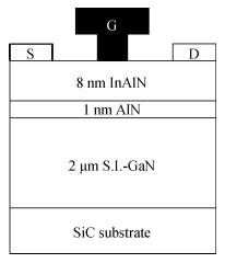
J. Semicond. > 2016, Volume 37 > Issue 2 > 024007

SEMICONDUCTOR DEVICES

70-nm-gated InAlN/GaN HEMTs grown on SiC substrate with fT/fmax > 160 GHz

Tingting Han1, Shaobo Dun1, Yuanjie Lü1, Guodong Gu2, Xubo Song2, Yuangang Wang2, Peng Xu2 and Zhihong Feng1,

+ Author Affiliations

 Corresponding author: Corresponding author. Email: ga917vv@163.com

DOI: 10.1088/1674-4926/37/2/024007

PDF

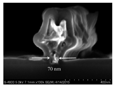
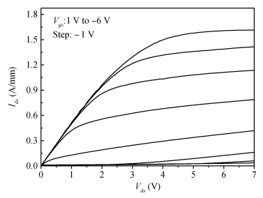
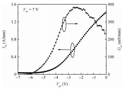
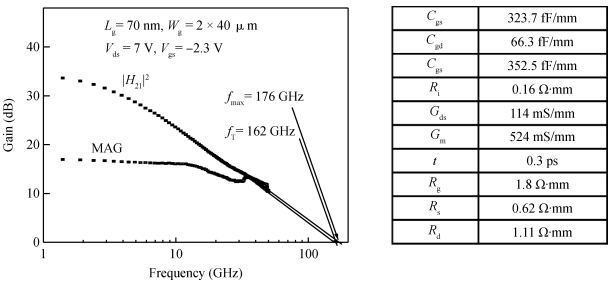
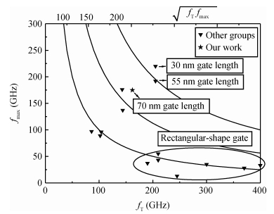
Abstract: InAlN/GaN high-electron-mobility transistors (HEMTs) on SiC substrate were fabricated and characterized. Several techniques, consisting of high electron density, 70 nm T-shaped gate, low ohmic contacts and a short drain-source distance, are integrated to gain high device performance. The fabricated InAlN/GaN HEMTs exhibit a maximum drain saturation current density of 1.65 A/mm at Vgs = 1 V and a maximum peak transconductance of 382 mS/mm. In addition, a unity current gain cut-off frequency (fT) of 162 GHz and a maximum oscillation frequency (fmax) of 176 GHz are achieved on the devices with the 70 nm gate length.

Key words: InAlN/GaNhigh-electron-mobility transistors (HEMTs)T-shaped gatecurrent gain cut-off frequency (fT)maximum oscillation frequency (fmax)

The energy issue is a hot topic in today’s world. With the reduction of non-renewable energy, people turned their attention to the development and utilization of new energy sources. Harvesting energy from our ambient environment as a sustainable power source for these applications including sensors[1, 2], micro/nano-system, environmental monitoring[3], medical science[4, 5], personal electronics[6, 7], and defense technology[8] has attracted increasing interest. Various approaches for scavenging mechanical energy in the surrounding environment have been developed and they are based on piezoelectrics[915], electrom agnetics[16, 17], and electrostatics[18, 19]. The recently invented triboelectric nanogenerator (TENG)[2026] provides an effective approach to convert mechanical energy into electricity by a conjunction of triboelectrification and electrostatic induction. So far, there are mainly two friction modes of TENGs: vertical contact-separation[27, 28], in-plane sliding[29, 30]. Except for the electric output of the disk or cylindrical rotating TENG is a similar sinusoidal signal, the output of the others are discontinuous and alternating short pulse which has the common characteristic of high voltage but low current and power[31]. The output voltage of TENGs, which is always up to several hundred volts, is extremely much higher than commercial electronics’ operating voltage that is generally just a few volts. However, the traditional step-down technology by using a transformer is not applicable for TENGs because the output power of the vast majority of TENGs just stay in the milliwatt power level and the transformer’s consumption of power is appreciable and mostly more than the output power of a TENG. Previous letters showed that we would get no energy output by using a transformer to reduce the output voltage except Zhu Guang’s two-dimensional planar-structured triboelectric nanogenerator that kept the maximum average output power record of 1.5 W[32]. Reported research and papers about TENGs focused on improving the output performance of TENGs. In contrast, the energy storage technologies of TENGs were rarely reported. So far, only several papers have reported the energy storage technologies of TENGs. Song developed an integrated self-charging power unit which stored energy in a flexible supercapacitor, but the supercapacitor connected to loads directly, so it could not provide stable voltage and regulate the value of output voltage[33]. All energy storage methods mentioned in these papers either have limitations or are complicated to operate and not practical. However, other related articles only stay at the stage of using triboelectric generators to charge the capacitor, but due to the unstable and low storage capacity of the capacitor, it is not suitable for direct power supply for commercial electronic products, and this will greatly restrict the practical application range of triboelectric generators. To solve this problem, we add an energy storage unit. The interface circuit is composed of six sections, namely a rectifier filter circuit, large-capacity electrolytic capacitors, a switching chip, a control chip, a charge management chip and a rechargeable lithium ion battery. The schematic circuit block diagram is shown in Fig. 1. Firstly, alternating current generated by triboelectric generators is processed to be stored in the electrolytic capacitors temporarily by the rectifier filter circuit. When the electric charge in the electrolytic capacitor is accumulated to a certain amount, the subsequent switch control circuit starts to work and charge the lithium-ion battery intermittently. The feasibility of the interface circuit is verified by experiment. Tests shows that the electricity generated by the triboelectric generator can be efficiently converted and stored in the electrolytic capacitor. When the capacitor’s voltage shoots to 5 V, the switch control system is driven, and the charging chip begins to work, so that the output electricity of the triboelectric generator is finally successfully stored in lithium-ion rechargeable batteries. It means that triboelectric generators can be a real application.

Figure  1.  (Color online) The schematic circuit block of the complete power management system.

In this work, we used a segmentally structured disk triboelectric nanogenerator that can harvest energy during both contact and non-contact modes. In contact mode, the TENG operates in the lateral sliding mode that is dominated by a parallel triboelectrification and electrostatic-induction process. In non-contact mode, the TENG relies on electrostatic induction for energy harvesting. The basic structure of the disk TENG is composed of two disk-shaped components with eighteen sectors each, as schematically illustrated in Fig. 2. It contains two circular poly(methyl methacrylate) (PMMA) sheets substrate, two electrode layers and one PTFE insulated layer. Eighteen fan-shaped Al foils are connected by an annular electrode as an electrode/induction layer. On the back side of the PTFE layer, a thick copper layer which serves as another electrode is deposited. Both parts can freely rotate in both contact and non-contact modes. During the process of spinning, the distance between the Al foil and the PTFE layer will change. As a result the switch between electrostatic-induction and triboelectrication can be achieved. All of the fan-shaped structures have the same diameter, inner diameter and radial angle.

Figure  2.  (Color online) (a) The photograph of the segmentally structured disk TENG. (b) The lateral view of the schematic structure of the segmentally structured disk TENG. (c) The sectional drawing of the schematic structure of the segmentally structured disk TENG.

The electric energy generation process can be explained by the coupling between triboelectric effect and electrostatic effect, as sketched in Fig. 3(a). When the two discs are separated at original position, TENG is in non-contact mode. Then the two rotating discs approach each other, and the induced charges will flow from Cu to Al and generate an electric current. The two discs will relatively rotate towards each other and generate extra triboelectric charges, hence two higher electric currents are induced when the two discs are in full contact. Afterwards the two discs begin to separate and another induced current is produced. Figs. 3(b) and 3(c) are respectively the open-circuit voltage curve and short-circuit current curve of the TENG. We can see that the peak current and voltage generated from contact mode are slightly higher than corresponding values from the non-contact mode because the amount of the transferring triboelectric charges is different. Due to the triboelectric charges remaining on the insulator surface for hours without much leakage, their subsequent induction is possible.

Figure  3.  (Color online) (a) The basic mechanism of electronic current generation process in a complete cycle. (b) The open-circuit voltage of the segmentally structured disk TENG. (c) The short-circuit current of the segmentally structured disk TENG.

The final purpose of research about TENGs is to drive commercial electronics with harvested ambient mechanical energy, or, in other words, realize industrialization. As for the energy conversion devices such as TENGs, there are generally two technical methods to use these devices as power sources. The first choice is using directly the pulses generated by energy conversion devices, such as LCDs. However, in many cases, the short AC pulses from TENGs, which have the common characteristic of high voltage but low current, cannot be applied to drive some commercial electronics directly, because the normal operation of many electronic products requires steady DC or the higher power than the power generated by TENGs. Therefore, it is necessary to regulate the output power by using a power management circuit. Meanwhile, in order to facilitate industrialization, the circuit should be composed of chips as much as possible. Some previous papers proposed using a capacitor as the final energy storage unit to supply power for electronics such as cell phones, however it should be noticed that the capacitor’s storage capacity is limited and its voltage is unstable when it discharges.

In order to solve these problems, this article employs a lithium ion battery (LIB) instead of a capacitor as the ultimate energy storage device. The complete interface circuit consists of a rectifier bridge, two filter capacitors, a large-capacity storage electrolytic capacitor, a control chip, a switch chip, a charging chip and a lithium ion battery. Fig. 4 is the schematic. The circuit will start to charge the LIB in regulation mode 480 s after the TENG begins to rotate.

Figure  4.  (Color online) The complete interface circuit schematic for triboelectric nanogenerator.

First, the rectifier bridge, consisting of four FR607 diodes whose reverse voltage is 1000 V, can be used in high-frequency applications. This is reasonable because the output of the TENG is a high-voltage short pulse AC signal and we do not use a step-down transformer. Then, it is noticed that the core difficulty for the interface circuit for the TENG is the low power output. Therefore the energy management circuit must use large capacity electrolytic capacitor as the primary energy storage device and the electrolytic capacitor discharge to drive the subsequent electricity system only when enough energy has been accumulated in it. For consideration of the high voltage of several hundred volts of pulsating DC, which is the rectified output of the TENG, and the need for enough energy to drive the follow-up chips, here we choose a model 450 V/680 μF electrolytic capacitor. Afterwards, the switch control circuit, which controls the electrolytic capacitor when to charge or discharge, is a key part. If there is no switch control circuit, no external load can be connected to the electrolytic capacitor because the consumption power of the load will most likely be greater than that generated by the TENG. In this paper, the integrated switch control circuit mainly consists of two chips, one is a double hysteresis comparator chip ICL7665 which serves as the control chip and provides high and low level voltage to the switch chip, the other is the switch chip CD4051 which controls whether the electrolytic capacitor discharges to the subsequent circuit or not according to the change of the level of the received voltage signal. Their chip pins and electrical connections are shown in Fig. 4. We choose ICL7665 as the control chip for the reason that its power consumption is extremely low and its working voltage and current can be provided by the electrolytic capacitor directly. Moreover, we can set the discharge voltage of the electrolytic capacitor named threshold voltage by adjusting the resistance of R1, R2 and R3, for example the threshold voltage is set to 5 V in this article. When the voltage across the electrolytic capacitor reaches the threshold voltage of 5 V, the OUT1 outputs low level, otherwise when the electrolytic capacitor discharge to below 5 V, OUT1 outputs high level. The chip CD4051 is a low-power eight channel multiplexer which selects one channel from 1 to 8 to connect it with its output terminal O/I to serve as a switch when A, B, C input different binary signal. Thus, the switch control circuit is conductive only when the voltage across the electrolytic capacitor reaches up to the settled threshold voltage of 5 V. In the end, in order to realize that the TENG charges the LIB, we need a charging management chip which supports intermittent charging because the output of the TENG is commonly an AC pulse. The charging management chip CN3153 can exactly meet the above requirements because it is specially dedicated to charge a single lithium ion battery by using input voltage source whose output power is extremely low. Finally, we experimentally verify the feasibility of this circuit. The experiment showed that the interface circuit diagrammed in Fig. 4 can start to charge the LIB in regulation mode 480 s after the TENG began to rotate.

Based on the principles described above, we designed the circuit. The photograph is shown in Fig. 5(a). Through experiments, we got the contrastive charging curves of the electrolytic capacitor with and without charging circuit, as shown in Fig. 5(b). It can be seen from the figure that the charging rate slowed down and the voltage did not rise up any longer but only fluctuated up and down after it reached 5 V, if the electrolytic capacitor was not connected to charging management circuit. The reason is that the electrolytic capacitor discharges to the interface circuit at the same time while it charges the electrolytic capacitor. When the electrolytic capacitor was charged to 5 V which is the threshold voltage of the control chip, the red indicator light of the charging chip CN3153 was lit up, as shown in Fig. 5(c). It indicated that the charging management chip had been driven and began to charge the lithium ion battery. Because the instantaneous discharge power of the electrolytic capacitor was greater than the output power of the triboelectric generator, the electrolytic capacitor performed for discharging. Therefore the capacitor’s voltage soon dropped below the threshold voltage 5 V. It made the switch control circuit disconnect again, so that the charging chip stopped working. Then the electrolytic capacitor was charged to 5 V again and restarted driving the switching control circuit. It moved in cycles in this way, hence the voltage of the electrolytic capacitor fluctuated up and down around 5 V and the indicator light of the charging chip glinted intermittently. These proved the feasibility of the interface circuit, designed for the triboelectric generator, for intermittently charging the lithium ion battery. As a contrast, we added a transformer to our interface circuit between the TENG and the rectifier, but experiment showed that the voltage of the capacitor C3 almost could not increase because the transformer consumed almost all the output energy of the TENG. Therefore, the energy management circuit that we designed in this work has a much lower power consumption and has an absolute advantage in the energy harvesting from the low power TENG.

Figure  5.  (Color online) (a) A photograph of the real experimental circuit. (b) The contrastive charging curves of the electrolytic capacitor with and without charging circuit. (c) The red indicator light of the charging chip CN3063 was lit up.

This article reported an interface circuit for triboelectric nanogenerators. This circuit was able to intermittently store as low as milliwatt level energy output of triboelectric nanogenerators in a rechargeable lithium ion battery. It could reduce the power consumption of the circuit, increase the output power and improve the efficiency of energy conversion, so it make progress on the practical application and industrialization of triboelectric nanogenerators. It is a universal power management circuit for various types of triboelectric nanogenerators.


[1]
[2]
[3]
[4]
[5]
[6]
[7]
[8]
[9]
[10]
[11]
[12]
[13]
[14]
[15]
[16]
[17]
[18]
[19]
[20]
[21]
[22]
[23]
[24]
[25]
[26]
[27]
[28]
Fig. 1.  Schematic diagram of the InAlN/GaN heterostructure.

Fig. 2.  Cross-sectional SEM image of the 70-nm T-shaped gate.

Fig. 3.  Output characteristics of the InAlN/GaN HEMTs.

Fig. 4.  Transfer characteristics of the InAlN/GaN HEMTs.

Fig. 5.  Small signal RF performance of the InAlN/GaN HEMTs and the model parameters.

Fig. 6.  Comparison of measured fT and fmax in InAlN/GaN HEMTs from different groups.

[1]
[2]
[3]
[4]
[5]
[6]
[7]
[8]
[9]
[10]
[11]
[12]
[13]
[14]
[15]
[16]
[17]
[18]
[19]
[20]
[21]
[22]
[23]
[24]
[25]
[26]
[27]
[28]
  • Search

    Advanced Search >>

    GET CITATION

    shu

    Export: BibTex EndNote

    Article Metrics

    Article views: 2944 Times PDF downloads: 27 Times Cited by: 0 Times

    History

    Received: 08 July 2015 Revised: Online: Published: 01 February 2016

    Catalog

      Email This Article

      User name:
      Email:*请输入正确邮箱
      Code:*验证码错误
      Tingting Han, Shaobo Dun, Yuanjie Lü, Guodong Gu, Xubo Song, Yuangang Wang, Peng Xu, Zhihong Feng. 70-nm-gated InAlN/GaN HEMTs grown on SiC substrate with fT/fmax > 160 GHz[J]. Journal of Semiconductors, 2016, 37(2): 024007. doi: 10.1088/1674-4926/37/2/024007 ****T T Han, S B Dun, Y Lü, G D Gu, X B Song, Y G Wang, P Xu, Z H Feng. 70-nm-gated InAlN/GaN HEMTs grown on SiC substrate with fT/fmax > 160 GHz[J]. J. Semicond., 2016, 37(2): 024007. doi: 10.1088/1674-4926/37/2/024007.
      Citation:
      Tingting Han, Shaobo Dun, Yuanjie Lü, Guodong Gu, Xubo Song, Yuangang Wang, Peng Xu, Zhihong Feng. 70-nm-gated InAlN/GaN HEMTs grown on SiC substrate with fT/fmax > 160 GHz[J]. Journal of Semiconductors, 2016, 37(2): 024007. doi: 10.1088/1674-4926/37/2/024007 ****
      T T Han, S B Dun, Y Lü, G D Gu, X B Song, Y G Wang, P Xu, Z H Feng. 70-nm-gated InAlN/GaN HEMTs grown on SiC substrate with fT/fmax > 160 GHz[J]. J. Semicond., 2016, 37(2): 024007. doi: 10.1088/1674-4926/37/2/024007.

      70-nm-gated InAlN/GaN HEMTs grown on SiC substrate with fT/fmax > 160 GHz

      DOI: 10.1088/1674-4926/37/2/024007
      Funds:

      Project supported by the National Natural Science Foundation of China (No. 61306113).

      More Information
      • Corresponding author: Corresponding author. Email: ga917vv@163.com
      • Received Date: 2015-07-08
      • Accepted Date: 2015-08-14
      • Published Date: 2016-01-25

      Catalog

        /

        DownLoad:  Full-Size Img  PowerPoint
        Return
        Return