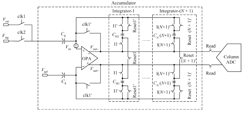
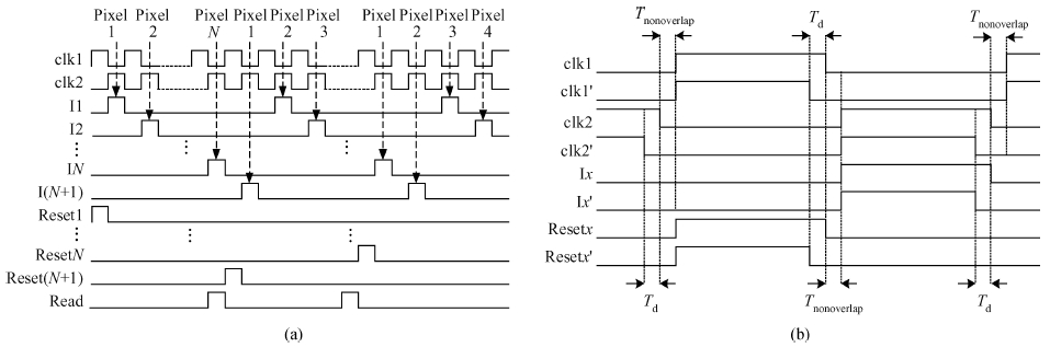
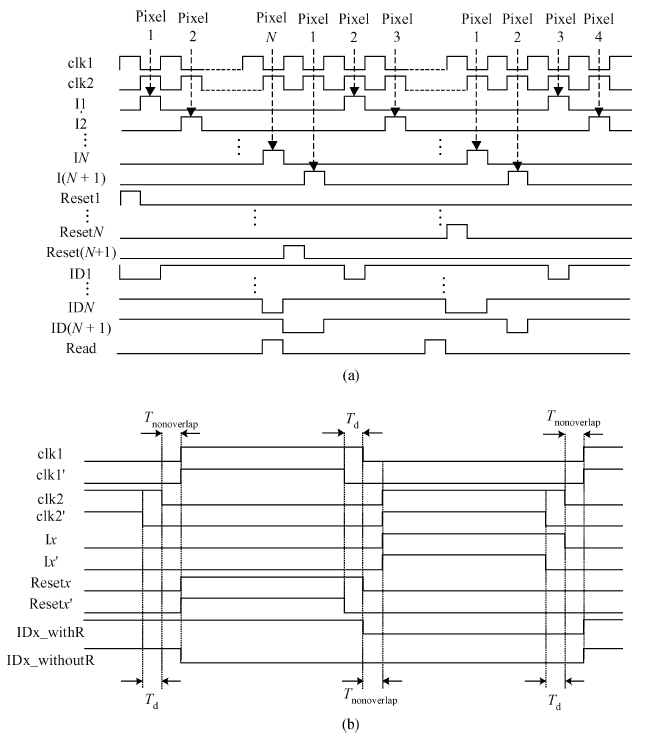
Processing math: 100%
J. Semicond. > 2016, Volume 37 > Issue 2 > 025001

SEMICONDUCTOR INTEGRATED CIRCUITS

High-stage analog accumulator for TDI CMOS image sensors

Jianxin Li, Fujun Huang, Yong Zong and Jing Gao

+ Author Affiliations

 Corresponding author: Jing Gao, Email: gaojing@tju.edu.cn

DOI: 10.1088/1674-4926/37/2/025001

PDF

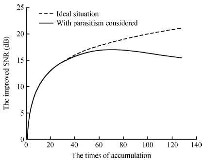
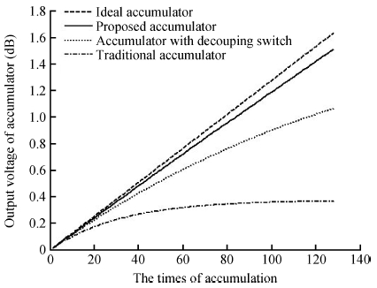
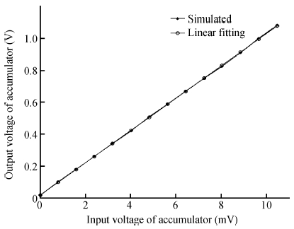
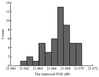
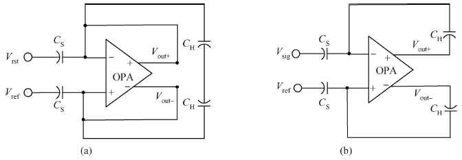
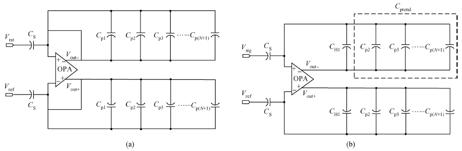
Abstract: The impact of the parasitic phenomenon on the performance of the analog accumulator in TDI CMOS image sensor is analyzed and resolved. A 128-stage optimized accumulator based on 0.18-μ m one-poly four-metal 3.3 V CMOS technology is designed and simulated. A charge injection effect from the top plate sampling is employed to compensate the un-eliminated parasitics based on the accumulator with a decoupling switch, and then a calibration circuit is designed to restrain the mismatch and Process, Voltage and Temperature (PVT) variations. The post layout simulation indicates that the improved SNR of the accumulator upgrades from 17.835 to 21.067 dB, while an ideal value is 21.072 dB. In addition, the linearity of the accumulator is 99.62%. The simulation results of two extreme cases and Monte Carlo show that the mismatch and PVT variations are restrained by the calibration circuit. Furthermore, it is promising to design a higher stage accumulator based on the proposed structure.

Key words: accumulatorsignal-to-noise ratio (SNR)time delay integration (TDI)CMOS image sensor (CIS)

Time delay integration (TDI) is a technology to improve the signal to noise ratio (SNR) by multiple sampling and signals accumulating,and it is widely used in applications where a line-scan system is required for high quality and low noise imaging even under low illumination conditions and at a high scanning speed[1, 2]. Since charge-coupled devices (CCDs) can accumulate the signal without noise,TDI is easy to realize by 2-D CCDs[3]. However,CCDs demand a high voltage supply,and can hardly integrate with the pixel signal processing circuit.

On the other hand,TDI CMOS image sensors (CIS) are gradually studied because of the development of CMOS in noise and dark current,etc.[4]. However,it is still the key for TDI CIS to design an accumulator with low-noise accumulation. Several reports on TDI CIS have been published recently. According to the exposure mode of pixels,TDI CIS can be divided into global shutter TDI CIS and rolling shutter TDI CIS. A global shutter TDI CIS is not the first option in TDI CIS,because the CDS operation cannot be adopted unless the transistors in pixel are more than five,which will result in a poor fill-factor and large pixel area. When the global shutter method is adopted,to get the high line readout speed,each TDI stage requires an individual amplifier and accumulation capacitors,which lead to the area increases,thus resulting in an increase in the price[5, 6]. When amplifiers and capacitors are integrated to the pixel,the pixel fill-factor will decrease seriously[7]. On the other hand,the CDS operation can be adopted in the rolling shutter TDI CIS,the column-level sharing amplifier can reduce the area and power consumption[8].

A 128-stage TDI CIS is designed[9],which is based on the rolling shutter structure[8]. It is shown that improved SNR for rolling shutter structure TDI CIS is limited by not only the noiseless accumulation but also the impact of layout parasitics of the accumulator[9]. Although the decoupling capacitor is added in the accumulator to decrease the impact of parasitics,the improved SNR reaches only 16.6 dB @ 128-stage,while it is 21.07 dB @ 128-stage in an ideal case[9]. Therefore,it is necessary to resolve the impact of parasitics completely in high-stage accumulators. To resolve the impact of parasitics,the decoupling switch and positive feedback capacitance compensation were employed in a previous design,but it limits the speed of the circuit. In this paper,a new accumulator structure based on the one presented[8] is proposed. The charge injection effect from the top plate sampling is employed to compensate the un-eliminated parasitics based on the accumulator with the decoupling switch. Then an additional calibration circuit is used to restrain the mismatch and process,voltage and temperature (PVT) variations. The result of post layout simulation indicates that the proposed accumulator is suitable for the design of high-stage TDI CIS.

The remainder of this paper is organized as follows. In Section 2,the principle of the proposed accumulator[8] and the impact of parasitic capacitance are introduced. In Section 3,an optimized accumulator is proposed. In Section 4,the post layout simulation results of the proposed accumulator are shown. A brief conclusion is drawn in Section 5.

The analog accumulator in the CMOS TDI image sensor[8] is shown in Figure 1,in which there are N+1 integrators,an operational amplifier (OPA) with the offset considered and the sample capacitor CS. Since the offset of the OPA due to the process variation is a very low-frequency noise,it can be modeled as a time-invariant voltage Vos as shown in Figure 1[10]. The N+1 integrators can realize N-stage signal accumulation in the N-stage CMOS TDI image sensor with a temporal oversampling rate of (N+1)/N[8, 11]. The common-mode noise including clock coupling,ground noise and charge injection will be restrained by the fully-differential topology. The timing diagram of the accumulator is shown in Figure 2,which is based on two-phase non-overlapping technology to avoid the signal dependent charge injections[12].

Figure  1.  The structure of the column parallel analog accumulator.
Figure  2.  The timing diagram of the accumulator. (a) All the controlling clocks. (b) The details of the controlling clocks.

Pixel noise and the offset of the OPA will be eliminated by the multi-stage switch-capacitor (SC) integrator. The first integrator of the accumulator is considered for an example to describe how the accumulator works as follows. The reset switch is closed by Reset1 and Reset1 to clear the charges stored in CH1 when the integrator is in the first sampling phase. Clk1 is closed to sample the pixel resetting signal Vrst and the OPA's input-referred offset Vos will be stored in the capacitor CS at the same time,as shown in Figure 3(a). In this phase,the output of the OPA is the output common mode voltage Vcom,out and the bottoms of the two holding capacitors have the same voltage VX. Then the integrator is in the integration phase when clk2 and I1 is closed to transfer the charges (VrstVsig)CS from CS to CH1 as shown in Figure 3(b). In this phase,the input common-mode voltage of the OPA is expressed as Vcom,in. Hence,the relation between the input and output of the first integrator can be expressed as:

(VrstVcom,outVos)CS+(VxVcom,outVos)CH=(VsigVcom,inVos)CS+(VoutVcom,inVos)CH(VrefVcom,out)CS+(VxVcom,out)CH=(VrefVcom,in)CS+(Vout+Vcom,in)CH}VoutVout+=CSCH(VrstVsig)\upDeltaVout(1)=CSCH\upDeltaVin\upDeltaVout(1)=VoutVout+,\upDeltaVin=VrstVsig.

(1)
Figure  3.  (a) The equivalent circuit during the first sampling phase. (b) The equivalent circuit during the holding phase.

After the N-th integration,the output of the first integrator can be expressed as:

\upDeltaVout[N]=\upDeltaVout[N1]+CSCH\upDeltaVin.

(2)

Because of the same holding capacitor in every integrator,Equation (2) is suitable for any integrator without considering mismatch. So the gain for any integrator in the accumulation can be got from Equation (2) as:

g[x]=\upDeltaVout[x]\upDeltaVout[x1]\upDeltaVin=CSCH.

(3)

Based on the TDI principle,SNRadd,which means the improved SNR,can be expressed as:

SNRadd=20lgNi=1g[i]Ni=1g2[i]=10lgN.

(4)

It can be seen from Equation (2) that the output of the accumulator does not include the pixel noise and offset of the OPA. At the same time,an ideal improved SNR is realized in Equation (4) without considering the impact of parasitics and the noise of the accumulator.

The thermal noise has set fundamental limits in the design of the analog circuits[13]. As analyzed in our previous work[8],with the assumption,CS=CH=C,the total thermal noise contributed by the accumulator can be expressed as:

¯VNtot=6N3kTC,

(5)

where k is the Boltzmann constant,and T is the absolute temperature. Therefore,the improved SNR of the accumulator will be smaller than the ideal ones due to the thermal noise. The layout parasitics of the accumulator will lower the effective number of accumulator stages; according to Equation (4),the improved SNR is also reduced[9]. The emphasis of this paper is to reduce the parasitics,and to improve the SNR,so the effect of noise is ignored in the next analysis.

The parasitics of the metal wires and vias in the layout design of the accumulator is the basic source which decreases the precision of the accumulator. The main parasitics include the internal parasitic capacitor of the holding capacitor,the parasitic capacitor of the input and output bus,and the parasitic capacitor of the OPA and sampling capacitance. Around the holding capacitor CH,there are more MOS switches,and the metal wire is more crowded relative to the sampling capacitor Cs. For the N-stage accumulator,the holding capacitor CH is located between the input and output bus. The parasitic capacitor of the holding capacitor CH is the main factor that influences the performance of the accumulator. The parasitic capacitor of the sampling capacitor Cs only affects the gain of the OPA and has little influence on the effective number of accumulator stages. Compared to the parasitic capacitor of the CH,the impact of the parasitic capacitor of Cs plays a negligible or minor role. We can restrain the impact of Cs by the symmetrical layout. Next we will analyse the parasitics of the CH and long bus in detail.

Because of the parasitics in the layout of the accumulator,there is a parasitic capacitor connected between the top or bottom plate of the holding capacitor in each integrator of the accumulator and the input or output of the OPA. The parasitic capacitors in the i-th integrator of the accumulator are shown in Figure 4. In Figure 4,the idle integrator can be equivalent to Cpi by Y-delta transformation[14].

{Cp12i=(Cpbbi×Cptti)/(Cpbbi+Cptti+CH)0,Cp23i=(Cptti×CH)/(Cpbbi+Cptti+CH)Cptti,Cp13i=(Cpbbi×CH)/(Cpbbi+Cptti+CH)Cpbbi.

(2)
Figure  4.  The equivalent circuits of the i -th idle integrator.

The parasitic capacitors Cp12i,Cp23i and Cp13i expressed as Equation (6) are the equivalent capacitors of CH,Cpbbi and Cptti. Therefore,the Cpi is:

Cpi=(Cp13i+Cptbi)(Cp23i+Cpbti)Cp13i+Cptbi+Cp12i+Cpbti+Cp12i(Cpbbi+Cptbi)(Cptti+Cpbti)Cpbbi+Cptbi+Cptti+Cpbti.

(7)

Therefore,the i-th idle integrator is equivalent to a parasitic capacitor Cpi. For analyzing the impact of parasitics,the models of the accumulator,where the 1st integrator is in the sampling phase or in the integration phase,are shown in Figures 5(a) and 5(b). In the sampling phase,the input and output of the OPA are reset by clk',so the charge in Cpi is cleared. In the integration phase,the lower plate of Cpi will get the charge from the sample capacitor,which decreases the gain of the accumulation. Furthermore,the higher the voltage on the top plate of CH1 is,the more charges the bottom plate of Cpi obtains.

Figure  5.  (a) The equivalent circuits of the accumulator in the sampling phase considering the parasitics. (b) The equivalent circuits of the accumulator in the holding phase considering the parasitics.

All the parasitic capacitances of the idle integrator are the same in the case of ignoring mismatch. Thus the total parasitic capacitor Cptotal can be expressed as:

Cptotal=NCpi.

(8)

Considering the parasitics analyzed above,the charge transfer relationship in Equation (2) changes to:

ΔVin×CS+ΔVout[N1]×CH=ΔVout[N]×(CH+Cptotal)ΔVout[N]=CSCH+CptotalΔVin+CHCH+CptotalΔVout[N1].

(9)

After the first integration of the first integrator,the differential output is:

\upDeltaVout[1]=CSCptotal+CH\upDeltaVin.

(10)

According to Equations (9) and (10),a common equation about the x-th integration of the first integrator can be expressed as:

Vout[x]=αVinxi=1Ki1,

(11)

where

α=CSCH+Cptotal,K=CHCH+Cptotal.

(12)

So the gain for any integrator in the accumulation can be expressed as:

g[x]=\upDeltaVout[x]\upDeltaVout[x1]\upDeltaVinαKx1.

(13)

Based on the TDI principle and Equation (13),the improved SNR with the parasitics considered can be expressed as:

SNRadd=20lgNi=1g[i]Ni=1g2[i]=10lg(1+K1K1KN1+KN).

(14)

When the parameter K is equal to 1,Equation (14) transforms to Equation (4). However,K is less than 1 because of the impact of parasitic capacitor Cptotal. Furthermore,while Cptotal increases with the accumulation stage,K gets worse. In order to show the parasitic phenomenon in the accumulator more directly,one integrator of the accumulator is designed and optimized with a 0.18 μm 1P4M CMOS technology,and the layout is shown in Figure 6.

Figure  6.  Layout of one integrator of the accumulator.

The parasitic capacitor Cpi in the layout is extracted and its capacitance is 0.449 fF,when the capacitance of the holding capacitor CH is 980 fF. Based on Equations (8),(12) and (14),the curve of the improved SNR versus the designed stage number of the accumulator can be derived,which is shown in Figure 7. From Figure 7,it can be seen that the parasitic phenomenon can lower the improved SNR dramatically,especially when the designed stage number is larger than 50,because the effective number of the accumulator stage becomes small significantly.

Figure  7.  The improved SNR versus the designed number of stage.

In order to make the proposed structure suitable for high-stage TDI CIS application,it is necessary to eliminate the impact of parasitics. In previous work[15],a small decoupling switch controlled by IDx is employed to decrease the impact of the parasitics of the integrator as shown in Figure 8. The timing diagram of the accumulator is shown in Figures 9(a) and 9(b).

Figure  8.  The i-th integrator with decoupling switch.
Figure  9.  The improved timing diagram of the accumulator. (a) All the controlling clocks. (b) The details of the controlling clocks.

Because of the decoupling switch,an alternating current (AC) ground is added to the bottom plate of the integrator capacitor in the equivalent circuit which is shown in Figure 10. When the decoupling switch is closed,the parasitic capacitors,Cptbi and Cpbti,etc.,which make great contributions to Cpi,will be equivalent to the loads of the input or the output of the OPA thanks to the AC ground. So the equivalent parasitic capacitor Cpi is changed to:

Cpi=Cp12i=CptbiCpbtiCptbi+Cpbti+CHi0.

(15)
Figure  10.  The equivalent circuits of the i -th idle integrator with decoupling switch.

However,the impacts which come from the parasitic capacitance of the sample switch,clk1',the non-ideal OPA and the parasitics of the bus cannot be eliminated in a simple way. Therefore,it is necessary to compensate the parasitics which cannot be eliminated for obtaining an accumulator with ideal performance.

In the previous design,the bottom plate sampling technology is used to eliminate the effect of channel charge injection. In this paper,the top plate sampling is applied for utilizing the charge injection of the top plate switch to compensate the parasitic capacitance. The schematic is shown in Figure 11. The two switching sequences on both sides of the holding capacitor are exchanged to realize the top plate sampling.

Figure  11.  Change in the i -th integrator.

Channel charge injection is analyzed that the MOS transistors with low W/L and the fast clock edge lead to equally distributing the charge across the switch[17]. In this situation,the charge injection of the top plate CMOS switch,\upDeltaQ,can be expressed as:

QN+=12(WL)NCox(VDDVout+)QN=12(WL)NCox(VDDVout)}\upDeltaQN=12(WL)NCox\upDeltaVoutQP+=12(WL)PCox(GNDVout+)QP=12(WL)PCox(GNDVout)}\upDeltaQP=12(WL)PCox\upDeltaVout}\upDeltaQ=\upDeltaQN+\upDeltaQP=12\upDeltaVoutCox[(WL)N+(WL)P],

(16)

where QN+ and QN are the injection charge which come from the NMOS transistor in the top plate switch,and QP+ and QP are the injection charge which come from the PMOS transistor in the top plate switch. In case of CH=CS,\upDeltaQ will be equally distributed to CH and CS. Thus,at the end of the integration phase,the change of the differential voltage in CH can be expressed as:

\upDeltaVout=\upDeltaVout+12\upDeltaQCH\upDeltaVout\upDeltaVout=1+14Cox[(WL)N+(WL)P]CH=CH+CS_eqCH,CS_eq=14Cox[(WL)N+(WL)P].

(17)

Thus the parameter K should be replaced by K as:

K=CHCH+CptotalCH+CSeqCH=CH+CSeqCH+Cptotal.

(18)

It can be seen in Equation (18) that the unique WL in MOS transistors of the top plate switch can realize K equaling to 1 when the top plate sampling is applied.

However,because of the threshold voltage of MOS transistors,the MOS transistors will be into the saturation region when the OPA has a large output. If the threshold voltages of NMOS and PMOS are VthN and VthP,respectively,Equation (16) should be changed to:

QN+=0,Vout+>VthNQN=12(WL)NCox(VDDVout)QP+=12(WL)PCox(GNDVout+)QP=0,Vout>VthP}\upDeltaQ=\upDeltaQN+\upDeltaQP=12\upDeltaVoutCox[(WL)N+(WL)P]12Cox[(WL)N(VDDVout+)+(WL)P(GNDVout)].

(19)

A simulation result about the increased voltage of the integrating capacitor in the top plate sampling versus the output voltage in the integrator is shown in Figure 12,which shows that a CMOS switch is not suitable as a linear compensation in the accumulator because of its nonlinear characteristics.

Figure  12.  The increased voltage after closing the top plate switch versus the output voltage of OPA.

The layout about the bootstrapped switch is shown in Figure 15,where the area of the integrator does not increase when the bootstrapped switch is added because of the column-sharing charge pump.

Figure  15.  Layout of the bootstrapped switch in an integrator.

The effect of the threshold voltage can be ignored in a bootstrapped switch. It should be noticed that the capacitance in the bootstrapped switch will occupy too much area if the bootstrapped switch is used in every integrator. Thus an implementation suitable for the TDI accumulator is shown in Figures 13 and 14,and the charge pump in Figure 14 is shared among the whole chip when the array is put into implementation. In Figure 13(a),when the i-th integrator is in the integration phase,four interaction MOS transistors are used to provide the controlled clock which reach up to bootstrapped voltage,Vb. When the i-th integrator is not in the integration phase,the controlled clock will close the current path from Vb voltage to ground completely,as shown in Figure 13(b) ,which will not affect the operation of the other integrators. As shown in Figure 14,Vb is generated from a charge pump controlled by generating two-phase non-overlapping clocks,where CB is a small capacitor which is used to preserve the bulk potential when switching[16].

Figure  13.  The operation principle of the bootstrapped switch proposed (a) when the i-th integrator is in the integration phase and (b) when the i-th integrator is not in the integration phase.
Figure  14.  The circuit of the bootstrapped voltage generator.

A simulation result about the change before and after closing the bootstrapped switch versus the output voltage in the integrator is shown in Figure 16. The linearity of the curve can be defined by the following:

Linearity=(1\upDeltaVmaxVmax)×100%,

(20)

where Vmax is the accumulator's full scale output and \upDeltaVmax is the maximum difference between the simulation and fitted transmission curves. So the linearity of the proposed bootstrapped switch is over 99.99%.

Figure  16.  The increased voltage of the integrating capacitor in the top plate sampling versus the bootstrapped switch versus the output of OPA.

In fact,the extracted parasitics are unreliable because of the process variation and mismatch. Thus a certain WL of the bootstrapped switch cannot guarantee realizing an ideal accumulator. The higher the stages of the accumulator are,the closer to 1 the parameter K must be. For 1% deviation in SNR,the variation of K cannot exceed 0.5‰. However,it is impossible to regulate the WL of the MOS transistors in a chip.

A correction technology for the uncertain parasitics is used in this paper. Here over-compensation in the bootstrapped switch,meaning a larger WL of the bootstrapped switch than the theoretical value,is applied. At the same time,a correction circuit for surplus compensation is designed as shown in Figure 17,in which four capacitors that increase double are added between the input and the output of the OPA; whether they are involved in the accumulator is easily decided by the digital codes from B1 to B4,which come from a 4-bit counter triggered by Cal.Bit. So the parameter K is changed to K:

K=CH+Cs_eqCH+Ctotal+Cadd,

(21)

where Cadd is the capacitor enabled in the calibration circuit. Further,it can be deduced that for a Cadd variation,the change in K can be expressed as:

\upDeltaKK=KCadd\upDeltaCaddK=(CH+Cs_eq)\upDeltaCadd(CH+Cptotal+Cadd)2K\upDeltaCaddCH.

(22)
Figure  17.  The correction circuit.

When \upDeltaCadd = 1 fF,the change in K can be controlled in less than 0.1%,which can meet the requirements for an 800-stages accumulator with SNR declining up to 1%. On the other hand,the correction circuit can work when the parasitic capacitance extracted has 1% error compared to an actual situation. The smaller \upDeltaCadd is designed,the more precise K can be achieved. While the more capacitors are added,the better parasitic variation can be restrained. The layout coming from Figure 17 is shown in Figure 18,where the capacitors in the calibration circuit are realized through the parasitics between metals for decreasing the mismatch.

Figure  18.  Layout of the correction circuit.

A 128-stage optimized accumulator suitable for TDI CIS is designed based on 0.18-μm one-poly four-metal 3.3 V CMOS technology. The capacitors used in the proposed accumulator are all metal-insulator-metal (MIM) capacitors with unit-area capacitance of 2 fF/μm2,and the size of one accumulator channel is 0.03 × 11.25 mm2 (each stage's size is 30 × 80 μm2). The post layout simulations about the proposed accumulator are demonstrated as follows.

The curves of the output of the accumulator versus the times of the accumulation are shown in Figure 19,where the results of a traditional accumulator and the optimized accumulator are both given as a comparison. The improved SNR which is based on Equation (14) is 21.0670 dB for the proposed accumulator,20.8404 dB for the accumulator with the decoupling switch and 17.8349 dB for the traditional accumulator,while the ideal value is 21.0721 dB. The effective times of accumulation,Neff,can be expressed as:

SNRadd=20lg102NeffNeff=10SNRadd10.

(23)
Figure  19.  The output curves of the accumulators @ 6.4 mV.

So the effective times of accumulation proposed is in 127.85 stages.

To evaluate the accumulator's linearity,its outputs are simulated when the inputs are increasing linearly,the result and the linear fitting curve are shown in Figure 20. The linearity of the accumulator can be defined by Equation (20),where \upDeltaVmax is the maximum difference between the simulated and fitted transmission curves. So the linearity of the accumulator is 99.62%,which is based on the result in Figure 20.

Figure  20.  Outputs of the accumulator with linearly inputs.

The calibration circuit for the mismatch and process variations is verified in this paper. The curves of the outputs of accumulators versus the times of the accumulation for different calibration codes are shown in Figure 21. Due to the restraint of the OPA's maximum output voltage,the voltage gets into saturation when the time of accumulation is high and the calibration code is low. The improved SNR for each calibration code is described in Table 1,so the most suitable calibration code can be achieved. According to Equation (14),only when the parameter K= 1 can we achieve the maximum signal-to-noise ratio and in other conditions,the more deviation from 1 the parameter K is,the smaller the signal-to-noise ratio is. When the top plate sampling in Figure 11 and the calibration circuit in Figure 17 are employed,the parameter K is changed to Equation (21). According to Equation (21) and Table 1,the value of K is close to 1 with the increase of code,until the code is 1001. Then the K will be less than 1. So the SNR changes in this way with the code.

Figure  21.  The curves of the output of accumulators versus the times of the accumulation for different calibration codes @ 6.4 mV.
Table  1.  The improved SNR for each calibration code.
DownLoad: CSV  | Show Table

A simulation result about the best fast case (fast process,lowest temperature,high voltage and minimum parasitic extraction) is shown in Figure 22(a) when the calibration code is 1101,and a simulation result about the worst slow case (slow process,high temperature,lowest voltage and maximum parasitic extraction) is shown in Figure 22(b) when the calibration code is 0011. The input voltage used in the worst slow case is halved because the output swing of OPA is restrained. In the two cases,the improved SNRs are 21.0574 and 21.0603 dB respectively,which shows the PVT variations are restrained by changing the calibration code. The mismatch is considered in the Monte Carlo simulation and the result is shown in Figure 23,where different calibration codes are used to obtain the best improved SNR. It should be noted that,in order to improve the simulation speed,the layout netlists of idle integrators are replaced by the capacitance model in the Monte Carlo simulation. However,the result still proves that the calibration circuit improves the mismatch to a certain degree.

Figure  22.  Simulation results in two extreme cases. (a) Best fast case. (b) Worst slow case. (@ 6.4 mV).
Figure  23.  Results of Monte Carlo simulation @ 6.4 mV.

In this paper,the impact of the parasitic phenomenon on the performance of an analog accumulator in the CMOS TDI image sensor is analyzed. In the basis,the impact of the parasitic phenomenon is decreased,eliminated and calibrated by the decoupling switch,the top plate sampling and calibration circuit respectively. A 128-stage optimized accumulator is designed based on 0.18-μm one-poly four-metal 3.3 V CMOS technology. The improved SNR of the proposed accumulator is obtained above 21.0574 dB in any situation. The linearity of the accumulator is 99.62% at the same time. The post layout simulation results have proved the effectiveness of the improvement for the accumulator when combating the parasitic phenomenon in the analog accumulator. Furthermore,it is possible to design a higher stage accumulator based on the proposed structure.


[1]
[2]
[3]
[4]
[5]
[6]
[7]
[8]
[9]
[10]
[11]
[12]
[13]
[14]
[15]
[16]
[17]
Fig. 1.  The structure of the column parallel analog accumulator.

Fig. 2.  The timing diagram of the accumulator. (a) All the controlling clocks. (b) The details of the controlling clocks.

Fig. 3.  (a) The equivalent circuit during the first sampling phase. (b) The equivalent circuit during the holding phase.

Fig. 4.  The equivalent circuits of the i -th idle integrator.

Fig. 5.  (a) The equivalent circuits of the accumulator in the sampling phase considering the parasitics. (b) The equivalent circuits of the accumulator in the holding phase considering the parasitics.

Fig. 6.  Layout of one integrator of the accumulator.

Fig. 7.  The improved SNR versus the designed number of stage.

Fig. 8.  The i-th integrator with decoupling switch.

Fig. 9.  The improved timing diagram of the accumulator. (a) All the controlling clocks. (b) The details of the controlling clocks.

Fig. 10.  The equivalent circuits of the i -th idle integrator with decoupling switch.

Fig. 11.  Change in the i -th integrator.

Fig. 12.  The increased voltage after closing the top plate switch versus the output voltage of OPA.

Fig. 15.  Layout of the bootstrapped switch in an integrator.

Fig. 13.  The operation principle of the bootstrapped switch proposed (a) when the i-th integrator is in the integration phase and (b) when the i-th integrator is not in the integration phase.

Fig. 14.  The circuit of the bootstrapped voltage generator.

Fig. 16.  The increased voltage of the integrating capacitor in the top plate sampling versus the bootstrapped switch versus the output of OPA.

Fig. 17.  The correction circuit.

Fig. 18.  Layout of the correction circuit.

Fig. 19.  The output curves of the accumulators @ 6.4 mV.

Fig. 20.  Outputs of the accumulator with linearly inputs.

Fig. 21.  The curves of the output of accumulators versus the times of the accumulation for different calibration codes @ 6.4 mV.

Fig. 22.  Simulation results in two extreme cases. (a) Best fast case. (b) Worst slow case. (@ 6.4 mV).

Fig. 23.  Results of Monte Carlo simulation @ 6.4 mV.

Table 1.   The improved SNR for each calibration code.

DownLoad: CSV
[1]
[2]
[3]
[4]
[5]
[6]
[7]
[8]
[9]
[10]
[11]
[12]
[13]
[14]
[15]
[16]
[17]
1

Precision photonic integration for future large-scale photonic integrated circuits

Xiangfei Chen

Journal of Semiconductors, 2019, 40(5): 050301. doi: 10.1088/1674-4926/40/5/050301

2

Column readout circuit with improved offset mismatch and charge sharing for CMOS image sensor

Zhongjie Guo, Ningmei Yu, Longsheng Wu

Journal of Semiconductors, 2019, 40(12): 122404. doi: 10.1088/1674-4926/40/12/122404

3

Large signal and noise properties of heterojunction AlxGa1-xAs/GaAs DDRIMPATTs

Suranjana Banerjee, Monojit Mitra

Journal of Semiconductors, 2016, 37(6): 064002. doi: 10.1088/1674-4926/37/6/064002

4

Modeling and simulation of single-event effect in CMOS circuit

Suge Yue, Xiaolin Zhang, Yuanfu Zhao, Lin Liu

Journal of Semiconductors, 2015, 36(11): 111002. doi: 10.1088/1674-4926/36/11/111002

5

Reset noise reduction through column-level feedback reset in CMOS image sensors

Li Binqiao, Xu Jiangtao, Xie Shuang, Sun Zhongyan

Journal of Semiconductors, 2011, 32(2): 025012. doi: 10.1088/1674-4926/32/2/025012

6

Wide dynamic range CMOS image sensor with in-pixel double-exposure and synthesis

Li Binqiao, Sun Zhongyan, Xu Jiangtao

Journal of Semiconductors, 2010, 31(5): 055002. doi: 10.1088/1674-4926/31/5/055002

7

A 0.5–1.7 GHz low phase noise ring-oscillator-based PLL for mixed-signal SoCs

Jiao Yishu, Zhou Yumei, Jiang Jianhua, Wu Bin

Journal of Semiconductors, 2010, 31(9): 095002. doi: 10.1088/1674-4926/31/9/095002

8

MEXTRAM model based SiGe HBT large-signal modeling

Han Bo, Li Shoulin, Cheng Jiali, Yin Qiuyan, Gao Jianjun, et al.

Journal of Semiconductors, 2010, 31(10): 104004. doi: 10.1088/1674-4926/31/10/104004

9

Two-dimensional pixel image lag simulation and optimization in a 4-T CMOS image sensor

Yu Junting, Li Binqiao, Yu Pingping, Xu Jiangtao, Mou Cun, et al.

Journal of Semiconductors, 2010, 31(9): 094011. doi: 10.1088/1674-4926/31/9/094011

10

A linear stepping PGA used in CMOS image sensors

Xu Jiangtao, Li Binqiao, Zhao Shibin, Li Hongle, Yao Suying, et al.

Journal of Semiconductors, 2009, 30(2): 025003. doi: 10.1088/1674-4926/30/2/025003

11

CMOS current controlled fully balanced current conveyor

Wang Chunhua, Zhang Qiujing, Liu Haiguang

Journal of Semiconductors, 2009, 30(7): 075009. doi: 10.1088/1674-4926/30/7/075009

12

Accurate and fast table look-up models for leakage current analysis in 65 nm CMOS technology

Xue Jiying, Li Tao, Yu Zhiping

Journal of Semiconductors, 2009, 30(2): 024004. doi: 10.1088/1674-4926/30/2/024004

13

A 10bit 50MS/s Pipeline ADC Design for a Million Pixels Level CMOS Image Sensor

Zhu Tiancheng, Yao Suying, Yuan Xiaoxing, Li Binqiao

Journal of Semiconductors, 2008, 29(10): 1939-1946.

14

Design,Analysis,and Optimization of a CMOS Active Pixel Sensor

Xu Jiangtao, Yao Suying, Li Binqiao, Shi Zaifeng, Gao Jing, et al.

Chinese Journal of Semiconductors , 2006, 27(9): 1548-1551.

15

A Novel Offset-Cancellation Technique for Low Voltage CMOS Differential Amplifiers

Han Shuguang, Chi Baoyong, Wang Zhihua

Chinese Journal of Semiconductors , 2006, 27(5): 778-782.

16

Elmore Delay Estimation of Two Adjacent Coupling Interconnects

Dong Gang, Yang Yintang, Li Yuejin

Chinese Journal of Semiconductors , 2006, 27(1): 54-58.

17

Design of a Monolithic CMOS LC-Voltage Controlled Oscillator with Low Phase Noise for 4GHz Frequency Synthesizers

Tang Lu, Wang Zhigong, Huang Ting, Li Zhiqun

Chinese Journal of Semiconductors , 2006, 27(3): 459-466.

18

A New CMOS Image Sensor with a High Fill Factor and the Dynamic Digital Double Sampling Technique

Liu Yu, Wang Guoyu

Chinese Journal of Semiconductors , 2006, 27(2): 313-317.

19

A 4.8GHz CMOS Fully Integrated LC Balanced Oscillator with Symmetrical Noise Filter Technique and Large Tuning Range

Yang Fenglin, Zhang Zhaofeng, Li Baoqi, and Min Hao

Chinese Journal of Semiconductors , 2005, 26(3): 448-454.

20

Noise Analysis of Analog Correlator

Tu Chunjiang, Liu Bo’an,and Chen Hongyi

Chinese Journal of Semiconductors , 2005, 26(3): 480-486.

1. Semwal, S.K., Saxena, R.S. CMOS Implementation of Time Delay Integration (TDI) for Imaging Applications: A Brief Review. IETE Technical Review (Institution of Electronics and Telecommunication Engineers, India), 2019. doi:10.1080/02564602.2019.1677516
  • Search

    Advanced Search >>

    GET CITATION

    Jianxin Li, Fujun Huang, Yong Zong, Jing Gao. High-stage analog accumulator for TDI CMOS image sensors[J]. Journal of Semiconductors, 2016, 37(2): 025001. doi: 10.1088/1674-4926/37/2/025001
    J X Li, F J Huang, Y Zong, J Gao. High-stage analog accumulator for TDI CMOS image sensors[J]. J. Semicond., 2016, 37(2): 025001. doi: 10.1088/1674-4926/37/2/025001.
    shu

    Export: BibTex EndNote

    Article Metrics

    Article views: 2928 Times PDF downloads: 32 Times Cited by: 1 Times

    History

    Received: 08 June 2015 Revised: Online: Published: 01 February 2016

    Catalog

      Email This Article

      User name:
      Email:*请输入正确邮箱
      Code:*验证码错误
      Jianxin Li, Fujun Huang, Yong Zong, Jing Gao. High-stage analog accumulator for TDI CMOS image sensors[J]. Journal of Semiconductors, 2016, 37(2): 025001. doi: 10.1088/1674-4926/37/2/025001 ****J X Li, F J Huang, Y Zong, J Gao. High-stage analog accumulator for TDI CMOS image sensors[J]. J. Semicond., 2016, 37(2): 025001. doi: 10.1088/1674-4926/37/2/025001.
      Citation:
      Jianxin Li, Fujun Huang, Yong Zong, Jing Gao. High-stage analog accumulator for TDI CMOS image sensors[J]. Journal of Semiconductors, 2016, 37(2): 025001. doi: 10.1088/1674-4926/37/2/025001 ****
      J X Li, F J Huang, Y Zong, J Gao. High-stage analog accumulator for TDI CMOS image sensors[J]. J. Semicond., 2016, 37(2): 025001. doi: 10.1088/1674-4926/37/2/025001.

      High-stage analog accumulator for TDI CMOS image sensors

      DOI: 10.1088/1674-4926/37/2/025001
      Funds:

      Project supported by the National Natural Science Foundation of China (Nos. 61404090, 61434004).

      More Information
      • Corresponding author: Email: gaojing@tju.edu.cn
      • Received Date: 2015-06-08
      • Accepted Date: 2015-09-01
      • Published Date: 2016-01-25

      Catalog

        /

        DownLoad:  Full-Size Img  PowerPoint
        Return
        Return