


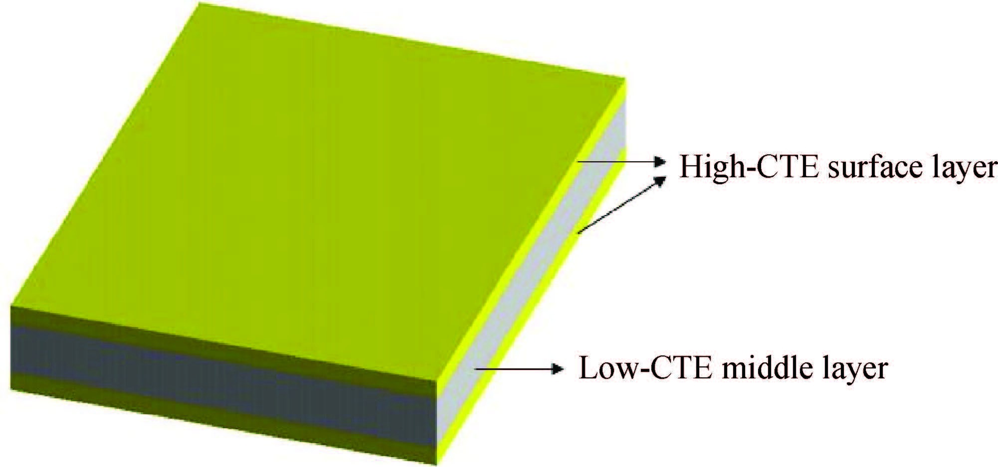
Fig. 1.
(Color online) Schematic diagram of the sandwich-structure submount.
SEMICONDUCTOR DEVICES
Yuxi Ni, Xiaoyu Ma, Hongqi Jing and Suping Liu
Corresponding author: Hongqi Jing, Email: jinghq@semi.ac.cn
Abstract: In order to improve the output power and increase the lifetime of laser diodes, expansion-matched submounts were investigated by finite element analysis. The submount was designed as sandwiched structure. By varying the vertical structure and material of the middle layer, the thermal expansion behavior on the mounting surface was simulated to obtain the expansion-matched design. In addition, the thermal performance of laser diodes packaged by different submounts was compared. The numerical results showed that, changing the thickness ratio of surface copper to middle layer will lead the stress and junction temperature to the opposite direction. Thus compromise needs to be made in the design of the vertical structure. In addition, the silicon carbide (SiC) is the most promising material candidate for the middle layer among the materials discussed in this paper. The simulated results were aimed at providing guidance for the optimal design of sandwich-structure submounts.
Keywords: high-power laser diodes, coefficient of thermal expansion, thermal management, finite element analysis
| [1] |
Zhang Zhike, Liu Yu, Liu Jianguo, et al. Packaging investigation of optoelectronic devices. Journal of Semiconductors, 2015, 36(10):101001
|
| [2] |
Jing Hongqi, Zhong Li, Ni Yuxi, et al. Design and simulation of a novel high-efficiency cooling heat-sink structure using fluid-thermodynamics. Journal of Semiconductors, 2015, 36(10):102006
|
| [3] |
Liu Yang, Leung S Y Y, Wong C K Y, et al. Thermal simulation of flexible LED package enhanced with copper pillars. Journal of Semiconductors, 2015, 36(6):064011
|
| [4] |
Paul C, Erbert G, Wenzel H, et al. Efficient high-power laser diodes. IEEE J of Sel Topics Quantum Electron, 2013, 19(4):1501211
|
| [5] |
Pliska A C, Mottin J, Matuschek N, et al. Bonding semiconductor laser chips:substrate material figure of merit and die attach layer influence. THERMINIC 2005, 2005:76
|
| [6] |
Dirk L, Hennig P. Highly thermally conductive substrates with adjustable CTE for diode laser bar packaging. MEMS/MOEMS:Advances in Photonic Communications, sensing, Metrology, Packaging and Assembly Proc SPIE, 2003, 4945:174
|
| [7] |
Liu Xingsheng, Zhao Wei, Xiong Lingling, et al. Packaging high power semiconductor lasers. New York:Springer, 2015
|
| [8] |
Schleuning D, Griffin M, James P. Robust hard-solder packaging of conduction cooled laser diode bars. High-Power Diode Laser Technology and Applications V, Proc SPIE, 2007, 6456:645604
|
| [9] |
Bezotosnyi V V, Krokhin O N, Oleshchenko, et al. Thermal modelling of high-power laser diodes mounted using various types of submounts. Quantum Electronics, 2014, 44(10):899
|
| [10] |
Miller R, Liu D, Horsinka M, et al. Composite-copper, low-thermal-resistance heat sinks for laser-diode bars, mini-bars and single-emitter devices. High-Power Diode Laser Technology and Applications VI, Proc SPIE, 2008, 6876:687607
|
| [11] |
Kitzmantel M, Neubauer E. Innovative hybrid heat sink materials with high thermal conductivities and tailored CTE, Components and Packaging for Laser Systems, Proc SPIE, 2015, 9346:934606
|
| [12] |
Suhir E. Predictive analytical thermal stress modeling in electronics and photonics. Applied Mechanics Reviews, 2009, 62(4):040801
|
| [13] |
Szymański M, Kozlowska A, Malag A, et al. Two-dimensional model of heat flow in broad-area laser diode mounted to a non-ideal heat sink. J Phys D, 2007, 40(3):924
|
| [14] |
Hostetler J L, Jiang C L, Negoita V, et al. Thermal and strain characteristics of high-power 940 nm laser arrays mounted with AuSn and In solders. High-Power Diode Laser Technology and Applications V, Proc SPIE, 2007, 6456:645602
|
| [15] |
Scholz C, Boucke K, Poprawe R. Mechanical stress-reducing heat sinks for high-power diode lasers. High-Power Diode Laser Technology and Applications Ⅱ, Proc SPIE, 2004, 5336:176
|
| [16] |
Szymanski M, Zbroszczyk M, Mroziewicz B. The influence of different heat sources on temperature distributions in broad-area diode lasers. Advanced Optoelectronics and Lasers, Proc SPIE, 2004, 5582:127
|
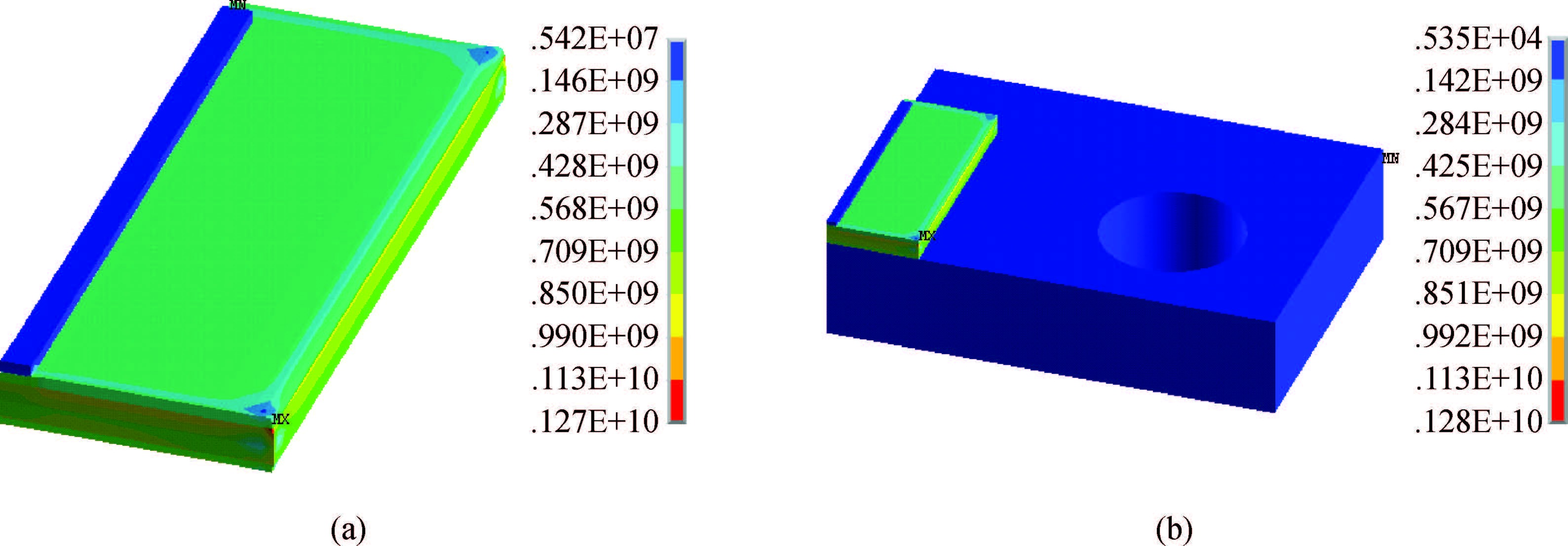


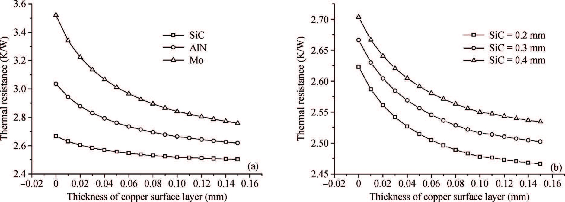
Table 1. Mechanical parameters in simulations.
| Material | CTE (ppm/K) | Elastic modulus\par (GPa) | Poission's ratio | Tensile stress (MPa) |
| GaAs | 6.03 | 85.3 | 0.312 | - |
| AuSn | 16 | 57 | 0.405 | 275 |
| In | 32 | 12.7 | 0.45 | 1.88 |
| Cu | 17 | 130 | 0.35 | - |
| SiC | 4.2 | 450 | 0.21 | - |
| AlN | 4.1 | 308 | 0.26 | - |
| Mo | 4.9 | 347 | 0.3 | - |
 DownLoad: CSV
Table 2. Detailed data on the structure and parameters of epitaxial layers.
| Layer | Composition | Thickness (μm) | Conductivity (W/m·K) |
| n-contact | Au | 0.4 | 318 |
| n-contact | AuGeNi | 0.2 | 150 |
| substrate | GaAs | 100 | 45 |
| n-cladding | Al0.36Ga0.64As | 1.2 | 12.52 |
| n-waveguide | Al0.25Ga0.75As | 0.65 | 15.23 |
| Quantum well | Ga0.84In0.16As | 0.01 | 9.898 |
| p-waveguide | Al0.25Ga0.75As | 0.65 | 15.23 |
| p-cladding | Al0.36Ga0.64As | 1.2 | 12.52 |
| p-cap | GaAs | 0.2 | 45 |
| Insulating layer | SiO2 | 0.2 | 1.28 |
| p-contact | Ti/Pt/Au | 0.3 | 318 |
| p-contact | Au | 0.4 | 318 |
| Solder | AuSn | 8 | 57 |
| Submount-top-layer | Cu | variable | 398 |
| Submount-middle-layer | SiC | 300 | 280 |
| Submount-middle-layer | AlN | 300 | 200 |
| Submount-middle-layer | Mo | 300 | 142 |
| Submount-bottom-layer | Cu | variable | 398 |
| Solder | In | 10 | 82 |
| F-mount | Cu | 2500 | 398 |
DownLoad: CSV
| [1] |
Zhang Zhike, Liu Yu, Liu Jianguo, et al. Packaging investigation of optoelectronic devices. Journal of Semiconductors, 2015, 36(10):101001
|
| [2] |
Jing Hongqi, Zhong Li, Ni Yuxi, et al. Design and simulation of a novel high-efficiency cooling heat-sink structure using fluid-thermodynamics. Journal of Semiconductors, 2015, 36(10):102006
|
| [3] |
Liu Yang, Leung S Y Y, Wong C K Y, et al. Thermal simulation of flexible LED package enhanced with copper pillars. Journal of Semiconductors, 2015, 36(6):064011
|
| [4] |
Paul C, Erbert G, Wenzel H, et al. Efficient high-power laser diodes. IEEE J of Sel Topics Quantum Electron, 2013, 19(4):1501211
|
| [5] |
Pliska A C, Mottin J, Matuschek N, et al. Bonding semiconductor laser chips:substrate material figure of merit and die attach layer influence. THERMINIC 2005, 2005:76
|
| [6] |
Dirk L, Hennig P. Highly thermally conductive substrates with adjustable CTE for diode laser bar packaging. MEMS/MOEMS:Advances in Photonic Communications, sensing, Metrology, Packaging and Assembly Proc SPIE, 2003, 4945:174
|
| [7] |
Liu Xingsheng, Zhao Wei, Xiong Lingling, et al. Packaging high power semiconductor lasers. New York:Springer, 2015
|
| [8] |
Schleuning D, Griffin M, James P. Robust hard-solder packaging of conduction cooled laser diode bars. High-Power Diode Laser Technology and Applications V, Proc SPIE, 2007, 6456:645604
|
| [9] |
Bezotosnyi V V, Krokhin O N, Oleshchenko, et al. Thermal modelling of high-power laser diodes mounted using various types of submounts. Quantum Electronics, 2014, 44(10):899
|
| [10] |
Miller R, Liu D, Horsinka M, et al. Composite-copper, low-thermal-resistance heat sinks for laser-diode bars, mini-bars and single-emitter devices. High-Power Diode Laser Technology and Applications VI, Proc SPIE, 2008, 6876:687607
|
| [11] |
Kitzmantel M, Neubauer E. Innovative hybrid heat sink materials with high thermal conductivities and tailored CTE, Components and Packaging for Laser Systems, Proc SPIE, 2015, 9346:934606
|
| [12] |
Suhir E. Predictive analytical thermal stress modeling in electronics and photonics. Applied Mechanics Reviews, 2009, 62(4):040801
|
| [13] |
Szymański M, Kozlowska A, Malag A, et al. Two-dimensional model of heat flow in broad-area laser diode mounted to a non-ideal heat sink. J Phys D, 2007, 40(3):924
|
| [14] |
Hostetler J L, Jiang C L, Negoita V, et al. Thermal and strain characteristics of high-power 940 nm laser arrays mounted with AuSn and In solders. High-Power Diode Laser Technology and Applications V, Proc SPIE, 2007, 6456:645602
|
| [15] |
Scholz C, Boucke K, Poprawe R. Mechanical stress-reducing heat sinks for high-power diode lasers. High-Power Diode Laser Technology and Applications Ⅱ, Proc SPIE, 2004, 5336:176
|
| [16] |
Szymanski M, Zbroszczyk M, Mroziewicz B. The influence of different heat sources on temperature distributions in broad-area diode lasers. Advanced Optoelectronics and Lasers, Proc SPIE, 2004, 5582:127
|


Article views: 4763 Times PDF downloads: 122 Times Cited by: 0 Times
Received: 12 October 2015 Revised: 13 January 2016 Online: Published: 01 June 2016
| Citation: |
Yuxi Ni, Xiaoyu Ma, Hongqi Jing, Suping Liu. Finite element analysis of expansion-matched submounts for high-power laser diodes packaging[J]. Journal of Semiconductors, 2016, 37(6): 064005. doi: 10.1088/1674-4926/37/6/064005
****
Y X Ni, X Y Ma, H Q Jing, S P Liu. Finite element analysis of expansion-matched submounts for high-power laser diodes packaging[J]. J. Semicond., 2016, 37(6): 064005. doi: 10.1088/1674-4926/37/6/064005.

|
| [1] |
Zhang Zhike, Liu Yu, Liu Jianguo, et al. Packaging investigation of optoelectronic devices. Journal of Semiconductors, 2015, 36(10):101001
|
| [2] |
Jing Hongqi, Zhong Li, Ni Yuxi, et al. Design and simulation of a novel high-efficiency cooling heat-sink structure using fluid-thermodynamics. Journal of Semiconductors, 2015, 36(10):102006
|
| [3] |
Liu Yang, Leung S Y Y, Wong C K Y, et al. Thermal simulation of flexible LED package enhanced with copper pillars. Journal of Semiconductors, 2015, 36(6):064011
|
| [4] |
Paul C, Erbert G, Wenzel H, et al. Efficient high-power laser diodes. IEEE J of Sel Topics Quantum Electron, 2013, 19(4):1501211
|
| [5] |
Pliska A C, Mottin J, Matuschek N, et al. Bonding semiconductor laser chips:substrate material figure of merit and die attach layer influence. THERMINIC 2005, 2005:76
|
| [6] |
Dirk L, Hennig P. Highly thermally conductive substrates with adjustable CTE for diode laser bar packaging. MEMS/MOEMS:Advances in Photonic Communications, sensing, Metrology, Packaging and Assembly Proc SPIE, 2003, 4945:174
|
| [7] |
Liu Xingsheng, Zhao Wei, Xiong Lingling, et al. Packaging high power semiconductor lasers. New York:Springer, 2015
|
| [8] |
Schleuning D, Griffin M, James P. Robust hard-solder packaging of conduction cooled laser diode bars. High-Power Diode Laser Technology and Applications V, Proc SPIE, 2007, 6456:645604
|
| [9] |
Bezotosnyi V V, Krokhin O N, Oleshchenko, et al. Thermal modelling of high-power laser diodes mounted using various types of submounts. Quantum Electronics, 2014, 44(10):899
|
| [10] |
Miller R, Liu D, Horsinka M, et al. Composite-copper, low-thermal-resistance heat sinks for laser-diode bars, mini-bars and single-emitter devices. High-Power Diode Laser Technology and Applications VI, Proc SPIE, 2008, 6876:687607
|
| [11] |
Kitzmantel M, Neubauer E. Innovative hybrid heat sink materials with high thermal conductivities and tailored CTE, Components and Packaging for Laser Systems, Proc SPIE, 2015, 9346:934606
|
| [12] |
Suhir E. Predictive analytical thermal stress modeling in electronics and photonics. Applied Mechanics Reviews, 2009, 62(4):040801
|
| [13] |
Szymański M, Kozlowska A, Malag A, et al. Two-dimensional model of heat flow in broad-area laser diode mounted to a non-ideal heat sink. J Phys D, 2007, 40(3):924
|
| [14] |
Hostetler J L, Jiang C L, Negoita V, et al. Thermal and strain characteristics of high-power 940 nm laser arrays mounted with AuSn and In solders. High-Power Diode Laser Technology and Applications V, Proc SPIE, 2007, 6456:645602
|
| [15] |
Scholz C, Boucke K, Poprawe R. Mechanical stress-reducing heat sinks for high-power diode lasers. High-Power Diode Laser Technology and Applications Ⅱ, Proc SPIE, 2004, 5336:176
|
| [16] |
Szymanski M, Zbroszczyk M, Mroziewicz B. The influence of different heat sources on temperature distributions in broad-area diode lasers. Advanced Optoelectronics and Lasers, Proc SPIE, 2004, 5582:127
|

 WeChat ID
Journal of Semiconductors © 2017 All Rights Reserved 京ICP备05085259号-2


