| [1] |
Amemiya Y, Suget T, Mizushima Y. Novel low loss and high speed diode utilizing an "ideal" ohmic contact. IEEE Trans Electron Devices, 1982, 29(2):236
|
| [2] |
Jayant B B. Analysis of a high voltage merged p-i-n/Schottky (MPS) rectifier. IEEE Electron Device Lett, 1987, EDL-8(9):407
|
| [3] |
Wang Ying, Yu Chenghao, Miao Zhikun, et al. Low leakage 4H-SiC junction barrier Schottky rectifier with sandwich p type well. IET Power Electron, 2015, 8(5):672
|
| [4] |
Ma Li, Gao Yong. A novel SiGe/Si heterojunction power diode utilizing an ideal ohmic contact. The Fourth International Workshop on Junction Technology (IWJT' 2004), 2004:263
|
| [5] |
Murray A F J, Kelleher A, Lane W A. On the use of a p+/n+ mosaic contact for fast switching diode applications. The Sixth International Conference on Power Electronics and Variable Speed Drives, Nottingham, UK, 1996:247
|
| [6] |
Aldrete V H E, Santana J, del Valle J L. Stored charge control of p-i-n diodes:a simulation approach. Fourth IEEE International Caracas Conference on Devices, Circuits and Systems, Oranjestad, Aruba, Dutch Caribbean, 2002:D021-1-8
|
| [7] |
Aldrete V H E, del Valle J L, Santana C J. A TCAD comparative study of power rectifiers-modified p-i-n vs. modified mosaic contact p-i-n diode. Microelectron Reliab, 2003, 43(1):181
|
| [8] |
Wu He, Wu Yu, Kang Baowei, et al. Simulation of power fast recovery diodes using local lifetime controlling technique. Chinese Journal of Semiconductors, 2003, 24(5):520
|
| [9] |
Humbel O, Galster N, Dalibor T, et al. Why is plasma engineering in fast recovery diodes by ion irradiation superior to emitter efficiency reduction. IEEE Trans Power Electron, 2003, 18(1):23
|
| [10] |
Wei Wensheng. Detection of carrier information in heterojunctions of nanocrystalline/crystalline Si. Solid State Sciences, 2010, 12(5):789
|
| [11] |
Chen X Y, Shen W Z. Observation of low-dimensional state tunneling in nanocrystalline silicon/crystalline silicon heterostructures. Appl Phys Lett, 2004, 85(5):287
|
| [12] |
Wei Wensheng, Zhao Ningning, Wang Tianmin. Conduction behavior of hydrogenated nanocrystalline silicon backward diode. Nanotechnology, 2006, 18(12):025203
|
| [13] |
Wei Wensheng, Wang Tianmin, Zhang Chunxi, et al. Variable capacitance diodes of (p)nc-Si:H/(n)c-Si heterojunction. Chinese Journal of Semiconductors, 2005, 26(4):745
|
| [14] |
Wei Wensheng, Yan Xunlei. Structural characterization of boron doped hydrogenated nanocrystalline silicon films. Vacuum, 2009, 83(5):787
|
| [15] |
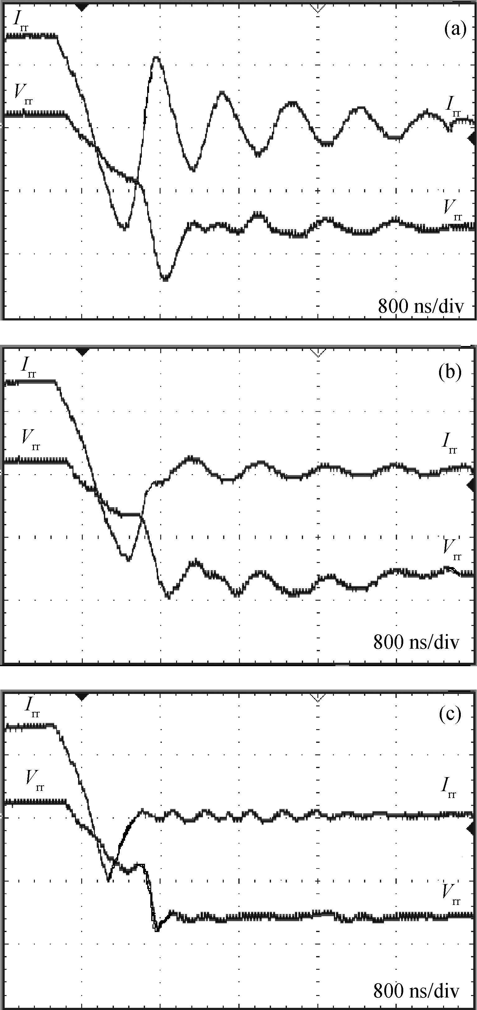
Wei Wensheng, Luo Fei, Zhang Chunxi, et al. Detection of reverse recovery characteristics of power diodes. IET Power Electronics, 2016, 9(3):476
|
| [16] |
Arpatzanis N, Tassis D, Dimitriadis C A, et al. Experimental investigation of noise in 4H-SiC p+-n-n+ junctions. Semicond Sci Technol, 2006, 21(3):591
|
| [17] |
Domeij M, Lutz J, Silber D. On the destruction limit of Si power diodes during reverse recovery with dynamic avalanche. IEEE Trans Electron Devices, 2003, 50(2):486
|
| [18] |
Pendharkar S P, Trivedi M, Shenai K. Dynamics of reverse recovery of high power p-i-n diodes. IEEE Trans Electron Devices, 1996, 43(1):142
|


 DownLoad: