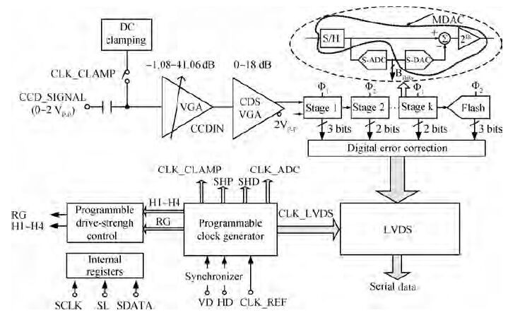
Fig. 1.
The block diagram of proposed CCD AFE.
SEMICONDUCTOR INTEGRATED CIRCUITS
Jingyu Wang, Zhangming Zhu and Shubin Liu
Corresponding author: Zhangming Zhu, Email: zhangmingzhu@xidian.edu.cn
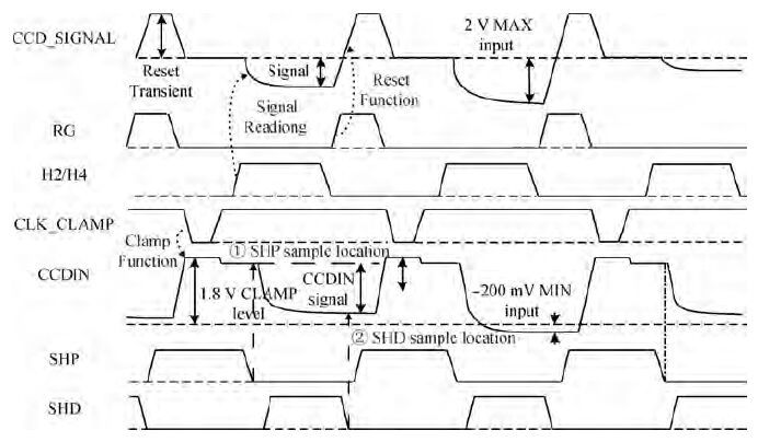
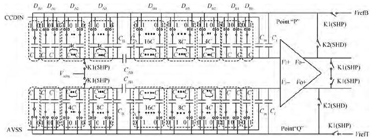
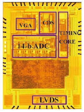
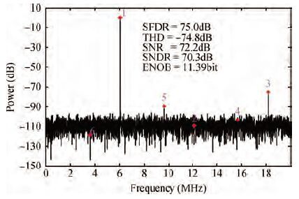
Abstract: A 14-bit, 40-MHz analog front end (AFE) for CCD scanners is analyzed and designed. The proposed system incorporates a digitally controlled wideband variable gain amplifier (VGA) with nearly 42 dB gain range, a correlated double sampler (CDS) with programmable gain functionality, a 14-bit analog-to-digital converter and a programmable timing core. To achieve the maximum dynamic range, the VGA proposed here can linearly amplify the input signal in a gain range from -1.08 to 41.06 dB in 6.02 dB step with a constant bandwidth. A novel CDS takes image information out of noise, and further amplifies the signal accurately in a gain range from 0 to 18 dB in 0.035 dB step. A 14-bit ADC is adopted to quantify the analog signal with optimization in power and linearity. An internal timing core can provide flexible timing for CCD arrays, CDS and ADC. The proposed AFE was fabricated in SMIC 0.18 μm CMOS process. The whole circuit occupied an active area of 2.8×4.8 mm2 and consumed 360 mW. When the frequency of input signal is 6.069 MHz, and the sampling frequency is 40 MHz, the signal to noise and distortion (SNDR) is 70.3 dB, the effective number of bits is 11.39 bit.
Keywords: analog front end, correlated double sampler, variable gain amplifier, ADC, programmable clock
| [1] |
Li Zhichao, Liu Yuntao, Chen Min, et al. A CMOS analog front-end chip for amperometric electrochemical sensors. Journal of Semiconductors, 2015, 36(7):075004
|
| [2] |
Ma Heping, Xu Hua, Chen Bei, et al. An ISM 2.4 GHz low power low-IF RF receiver front-end. Journal of Semiconductors, 2015, 36(8):085002
|
| [3] |
Liu Jialin, Zhang Xu, Hu Xiaohui, et al. A CMOS frontend chip for implantable neural recording with wide voltage supply range. Journal of Semiconductors, 2015, 36(10):105003
|
| [4] |
Wang Yanchao, Ke Keren, Qin Wenhui, et al. A low power low noise analog front end for portable healthcare system. Journal of Semiconductors, 2015, 36(10):105008
|
| [5] |
Zhang Hong, Zhang Jie, Zhang Mudan, et al. A multifunctional switched-capacitor programmable gain amplifier for high-definition video analog front-ends. Journal of Semiconductors, 2015, 36(3):035002
|
| [6] |
Garcia-Gonzalez J M, Greitschus N, Desel T. A 94-mW, 100-MS/s, 12-bit pipeline ADC for multi-standard TV demodulation applications. Analog Integrated Circuits and Signal Processing, 2010, 62(2):167
|
| [7] |
Chen Huabin, Xiang Jixuan, Xue Xiangyan, et al. An analog front end with a 12-bit 3.2-MS/s SAR ADC for a power line communication system. Journal of Semiconductors, 2014, 35(11):115008
|
| [8] |
Dai Lan, Liu Wenkai, Lu Yan. A 410μw, 70 dB SNR high performance analog front-end for portable audio application. Journal of Semiconductors, 2014, 35(10):115013
|
| [9] |
Chen Chengying, Hu Xiaoyu, Fan Jun, et al. A 55-dB SNDR, 2.2-mW double chopper-stabilized analog front-end for a thermopile sensor. Journal of Semiconductors, 2014, 35(05):055003
|
| [10] |
Marcelot O, Estribeau M, Goiffon V, et al. Study of CDD transport on CMOS imaging technology:comparison between SCCD and BCCD, and ramp effect on CTI. IEEE Trans Electron Device, 2014, 61(3):844
|
| [11] |
Djite I, Estribeau M, Magnan P, et al. Theoretical models of modulation transfer function, quantum efficiency, and crosstalk for CCD and CMOS image sensor. IEEE Trans Electron Devices, 2012, 59(3):729
|
| [12] |
Ahuja B, Huffman E G, Gower R L, et al. A 30Msample/s 12b 110mW video analog front end for digital camera. ISSCC Dig Tech Papers, 2002:438
|
| [13] |
Reynolds D, Ho S. An integrated 12 bit analog front end for CCD based image processing application. Symp VLSI Circuits Dig Tech Papers, 1996:96
|
| [14] |
Nitta S, Tanaka K. A 79 dB-SNR 70 mW 18 MHz CCD FRONT-END with full-digital amplification scheme. IEEE Trans Consum Electron, 2001, 47(3):459
|
| [15] |
You S B, Kim J W, Kim S. A CMOS 16-bit 20 MSPS analog front end for scanner/MFP applications. IEEE Trans Consumer Electron, 2003, 49(3):647
|
| [16] |
14-Bit CCD Signal Processor with Precision TimingTM Generator (AD9970) from Analog devices
|
| [17] |
Wang Wenbo, Mao Luhong, Xiao Xindong, et al. A differential automatic gain control circuit with two-stage -10 to 50 dB tuning range VGAs. Journal of Semiconductors, 2013, 34(2):025008
|
| [18] |
Chiu Y, Gray P R, Nikolic B. A 14-b 12-MS/s CMOS pipeline ADC with over 100-dB SFDR. IEEE J Solid-State Circuits, 2008, 39(12):2139
|
| [19] |
Yue Sen, Zhao Yiqiang, Pang Puilong, et al. A 14-bit 50 MS/s sample-and-hold circuit for pipelined ADC. Journal of Semiconductors, 2014, 35(5):055009
|


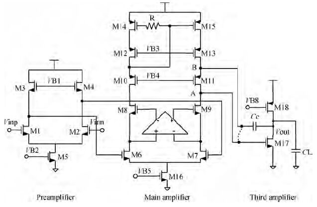
Table 1. Transistor sizes and element values for VGA amplifier.
| Amplifier | Transistors | w(μm) | l (μm) |
| Preamplifier | M1, M2 | 400 | 0.35 |
| M3, M4 | 20 | 0.35 | |
| M5 | 200 | 0.35 | |
| Main amplifier | M6, M7 | 120 | 0.2 |
| M8, M9 | 120 | 0.3 | |
| M10, M11 | 300 | 0.2 | |
| M12, M13 | 400 | 0.3 | |
| M14, M15 | 400 | 0.3 | |
| M16 | 300 | 0.2 | |
| Third amplifier | M17 | 50 | 0.35 |
| M18 | 290 | 0.3 | |
| Resistors: R= 200 Ω, Capacitors: Cc=800 fF |
 DownLoad: CSV
Table 2. Performance comparisons of CCD analog front end.
| Parameter | This work | Ref. [5] | Ref. [12] | Ref. [13] | Ref. [14] | Ref. [15] |
| Technology (μm) | 0.18 | 0.18 | 0.35 | 0.6 | N/A | 0.35 |
| Power supply (V) | 3(A)/1.8(D) | 1.8 | 2.7 | 5 | 2.7-3.6 | 3 |
| Resolution (bits) | 14 | N/A | 12 | 12 | 14 | 16 |
| Sampling rate (MHz) | 40 | 205 | 30 | 6 | 24 | 20 |
| Input range(V) | 2 | 1 | 1 | 4 | 0.9 | 2.4 |
| PGA gain range (dB) | -1.08 to 41 / 0-18 | -0.9 to 7 | 6-36 | 0-12 | -6 to 42 | 0-15.9 |
| Gain step (dB) | 6.02/0.035 | 0.017 | 0.05 | 0.75 | 0.5 | 1.32 |
| Programmable clock | 64 Phase | N/A | N/A | N/A | N/A | N/A |
| DNL (LSB) | ± 0.5 | N/A | ± 0.4 | ± 0.5 | ± 1.5 | +1.4/-0.9 |
| INL (LSB) | +2.5/-5 | N/A | N/A | ± 1 | ± 2 | +6.7/-17 |
| Power consumption (mW) | 360 | 18 | 110 | 450 | 70 | 300 |
| Active area (mm2) | 13.44 | 0.1 | 7.8 | 21.07 | N/A | 8.28 |
DownLoad: CSV
| [1] |
Li Zhichao, Liu Yuntao, Chen Min, et al. A CMOS analog front-end chip for amperometric electrochemical sensors. Journal of Semiconductors, 2015, 36(7):075004
|
| [2] |
Ma Heping, Xu Hua, Chen Bei, et al. An ISM 2.4 GHz low power low-IF RF receiver front-end. Journal of Semiconductors, 2015, 36(8):085002
|
| [3] |
Liu Jialin, Zhang Xu, Hu Xiaohui, et al. A CMOS frontend chip for implantable neural recording with wide voltage supply range. Journal of Semiconductors, 2015, 36(10):105003
|
| [4] |
Wang Yanchao, Ke Keren, Qin Wenhui, et al. A low power low noise analog front end for portable healthcare system. Journal of Semiconductors, 2015, 36(10):105008
|
| [5] |
Zhang Hong, Zhang Jie, Zhang Mudan, et al. A multifunctional switched-capacitor programmable gain amplifier for high-definition video analog front-ends. Journal of Semiconductors, 2015, 36(3):035002
|
| [6] |
Garcia-Gonzalez J M, Greitschus N, Desel T. A 94-mW, 100-MS/s, 12-bit pipeline ADC for multi-standard TV demodulation applications. Analog Integrated Circuits and Signal Processing, 2010, 62(2):167
|
| [7] |
Chen Huabin, Xiang Jixuan, Xue Xiangyan, et al. An analog front end with a 12-bit 3.2-MS/s SAR ADC for a power line communication system. Journal of Semiconductors, 2014, 35(11):115008
|
| [8] |
Dai Lan, Liu Wenkai, Lu Yan. A 410μw, 70 dB SNR high performance analog front-end for portable audio application. Journal of Semiconductors, 2014, 35(10):115013
|
| [9] |
Chen Chengying, Hu Xiaoyu, Fan Jun, et al. A 55-dB SNDR, 2.2-mW double chopper-stabilized analog front-end for a thermopile sensor. Journal of Semiconductors, 2014, 35(05):055003
|
| [10] |
Marcelot O, Estribeau M, Goiffon V, et al. Study of CDD transport on CMOS imaging technology:comparison between SCCD and BCCD, and ramp effect on CTI. IEEE Trans Electron Device, 2014, 61(3):844
|
| [11] |
Djite I, Estribeau M, Magnan P, et al. Theoretical models of modulation transfer function, quantum efficiency, and crosstalk for CCD and CMOS image sensor. IEEE Trans Electron Devices, 2012, 59(3):729
|
| [12] |
Ahuja B, Huffman E G, Gower R L, et al. A 30Msample/s 12b 110mW video analog front end for digital camera. ISSCC Dig Tech Papers, 2002:438
|
| [13] |
Reynolds D, Ho S. An integrated 12 bit analog front end for CCD based image processing application. Symp VLSI Circuits Dig Tech Papers, 1996:96
|
| [14] |
Nitta S, Tanaka K. A 79 dB-SNR 70 mW 18 MHz CCD FRONT-END with full-digital amplification scheme. IEEE Trans Consum Electron, 2001, 47(3):459
|
| [15] |
You S B, Kim J W, Kim S. A CMOS 16-bit 20 MSPS analog front end for scanner/MFP applications. IEEE Trans Consumer Electron, 2003, 49(3):647
|
| [16] |
14-Bit CCD Signal Processor with Precision TimingTM Generator (AD9970) from Analog devices
|
| [17] |
Wang Wenbo, Mao Luhong, Xiao Xindong, et al. A differential automatic gain control circuit with two-stage -10 to 50 dB tuning range VGAs. Journal of Semiconductors, 2013, 34(2):025008
|
| [18] |
Chiu Y, Gray P R, Nikolic B. A 14-b 12-MS/s CMOS pipeline ADC with over 100-dB SFDR. IEEE J Solid-State Circuits, 2008, 39(12):2139
|
| [19] |
Yue Sen, Zhao Yiqiang, Pang Puilong, et al. A 14-bit 50 MS/s sample-and-hold circuit for pipelined ADC. Journal of Semiconductors, 2014, 35(5):055009
|


Article views: 4361 Times PDF downloads: 79 Times Cited by: 0 Times
Received: 17 September 2015 Revised: 11 December 2015 Online: Published: 01 June 2016
| Citation: |
Jingyu Wang, Zhangming Zhu, Shubin Liu. A 14-bit 40-MHz analog front end for CCD application[J]. Journal of Semiconductors, 2016, 37(6): 065002. doi: 10.1088/1674-4926/37/6/065002
****
J Y Wang, Z M Zhu, S B Liu. A 14-bit 40-MHz analog front end for CCD application[J]. J. Semicond., 2016, 37(6): 065002. doi: 10.1088/1674-4926/37/6/065002.

|
| [1] |
Li Zhichao, Liu Yuntao, Chen Min, et al. A CMOS analog front-end chip for amperometric electrochemical sensors. Journal of Semiconductors, 2015, 36(7):075004
|
| [2] |
Ma Heping, Xu Hua, Chen Bei, et al. An ISM 2.4 GHz low power low-IF RF receiver front-end. Journal of Semiconductors, 2015, 36(8):085002
|
| [3] |
Liu Jialin, Zhang Xu, Hu Xiaohui, et al. A CMOS frontend chip for implantable neural recording with wide voltage supply range. Journal of Semiconductors, 2015, 36(10):105003
|
| [4] |
Wang Yanchao, Ke Keren, Qin Wenhui, et al. A low power low noise analog front end for portable healthcare system. Journal of Semiconductors, 2015, 36(10):105008
|
| [5] |
Zhang Hong, Zhang Jie, Zhang Mudan, et al. A multifunctional switched-capacitor programmable gain amplifier for high-definition video analog front-ends. Journal of Semiconductors, 2015, 36(3):035002
|
| [6] |
Garcia-Gonzalez J M, Greitschus N, Desel T. A 94-mW, 100-MS/s, 12-bit pipeline ADC for multi-standard TV demodulation applications. Analog Integrated Circuits and Signal Processing, 2010, 62(2):167
|
| [7] |
Chen Huabin, Xiang Jixuan, Xue Xiangyan, et al. An analog front end with a 12-bit 3.2-MS/s SAR ADC for a power line communication system. Journal of Semiconductors, 2014, 35(11):115008
|
| [8] |
Dai Lan, Liu Wenkai, Lu Yan. A 410μw, 70 dB SNR high performance analog front-end for portable audio application. Journal of Semiconductors, 2014, 35(10):115013
|
| [9] |
Chen Chengying, Hu Xiaoyu, Fan Jun, et al. A 55-dB SNDR, 2.2-mW double chopper-stabilized analog front-end for a thermopile sensor. Journal of Semiconductors, 2014, 35(05):055003
|
| [10] |
Marcelot O, Estribeau M, Goiffon V, et al. Study of CDD transport on CMOS imaging technology:comparison between SCCD and BCCD, and ramp effect on CTI. IEEE Trans Electron Device, 2014, 61(3):844
|
| [11] |
Djite I, Estribeau M, Magnan P, et al. Theoretical models of modulation transfer function, quantum efficiency, and crosstalk for CCD and CMOS image sensor. IEEE Trans Electron Devices, 2012, 59(3):729
|
| [12] |
Ahuja B, Huffman E G, Gower R L, et al. A 30Msample/s 12b 110mW video analog front end for digital camera. ISSCC Dig Tech Papers, 2002:438
|
| [13] |
Reynolds D, Ho S. An integrated 12 bit analog front end for CCD based image processing application. Symp VLSI Circuits Dig Tech Papers, 1996:96
|
| [14] |
Nitta S, Tanaka K. A 79 dB-SNR 70 mW 18 MHz CCD FRONT-END with full-digital amplification scheme. IEEE Trans Consum Electron, 2001, 47(3):459
|
| [15] |
You S B, Kim J W, Kim S. A CMOS 16-bit 20 MSPS analog front end for scanner/MFP applications. IEEE Trans Consumer Electron, 2003, 49(3):647
|
| [16] |
14-Bit CCD Signal Processor with Precision TimingTM Generator (AD9970) from Analog devices
|
| [17] |
Wang Wenbo, Mao Luhong, Xiao Xindong, et al. A differential automatic gain control circuit with two-stage -10 to 50 dB tuning range VGAs. Journal of Semiconductors, 2013, 34(2):025008
|
| [18] |
Chiu Y, Gray P R, Nikolic B. A 14-b 12-MS/s CMOS pipeline ADC with over 100-dB SFDR. IEEE J Solid-State Circuits, 2008, 39(12):2139
|
| [19] |
Yue Sen, Zhao Yiqiang, Pang Puilong, et al. A 14-bit 50 MS/s sample-and-hold circuit for pipelined ADC. Journal of Semiconductors, 2014, 35(5):055009
|

 WeChat ID
Journal of Semiconductors © 2017 All Rights Reserved 京ICP备05085259号-2