


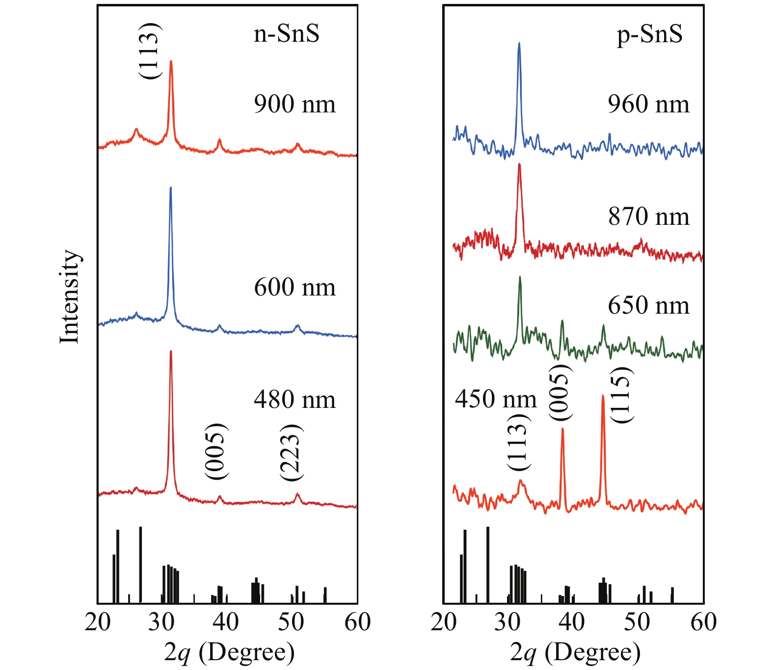
Fig. 1.
(Color online) X-ray diffractograms of n-type and p-type films along with powder pattern showing similar crystal structure.
SEMICONDUCTOR MATERIALS
Yashika Gupta1, 2 and P. Arun1,
Corresponding author: P. Arun, Email: arunp92@sgtbkhalsa.du.ac.in
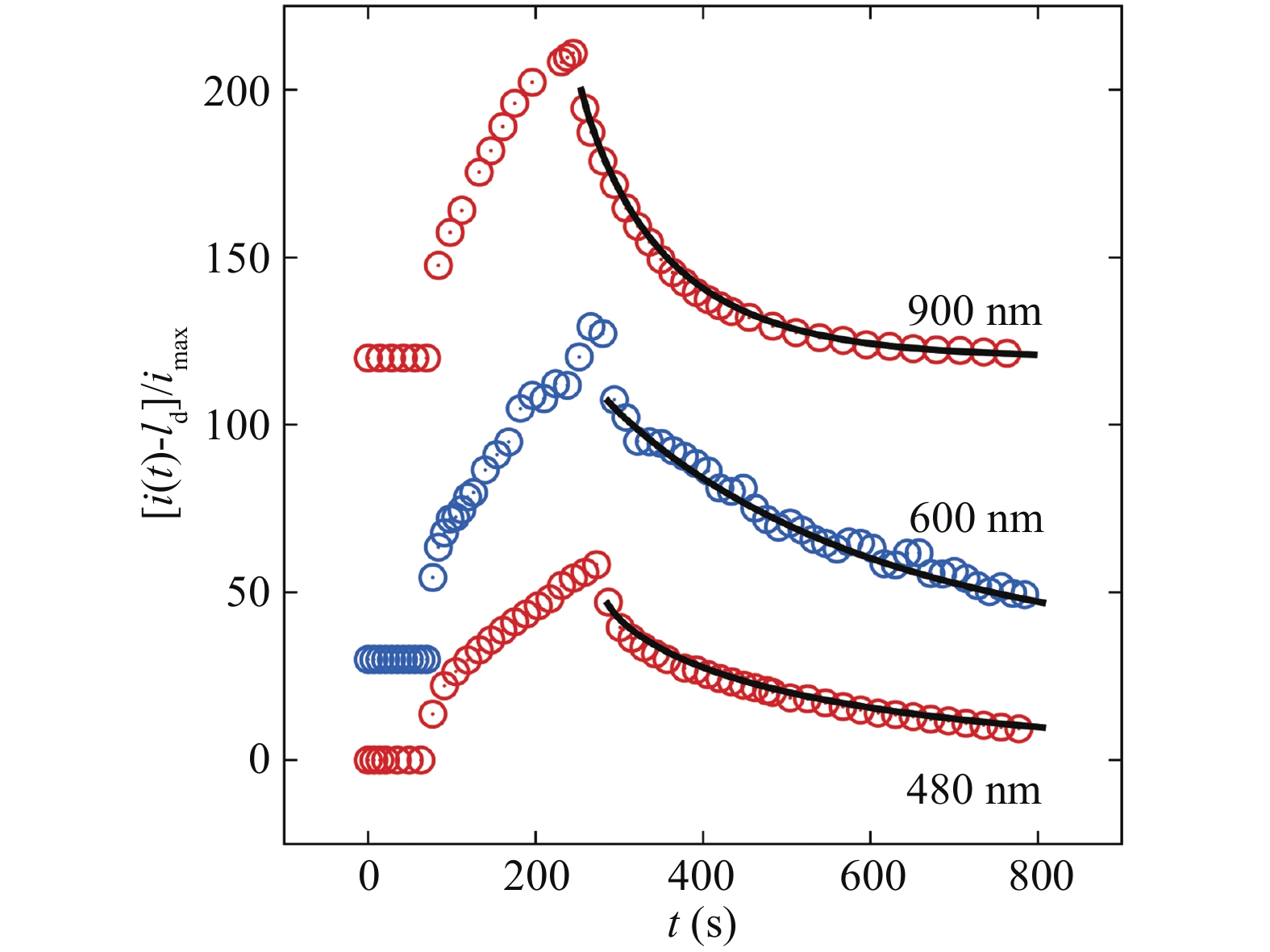
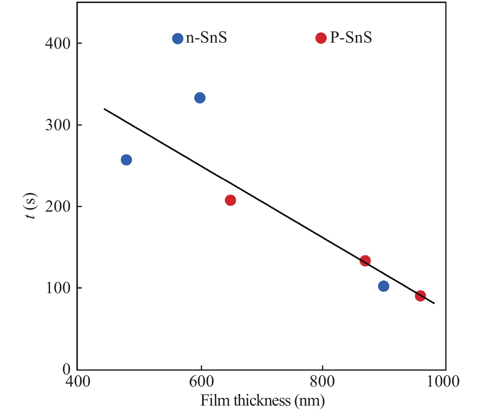
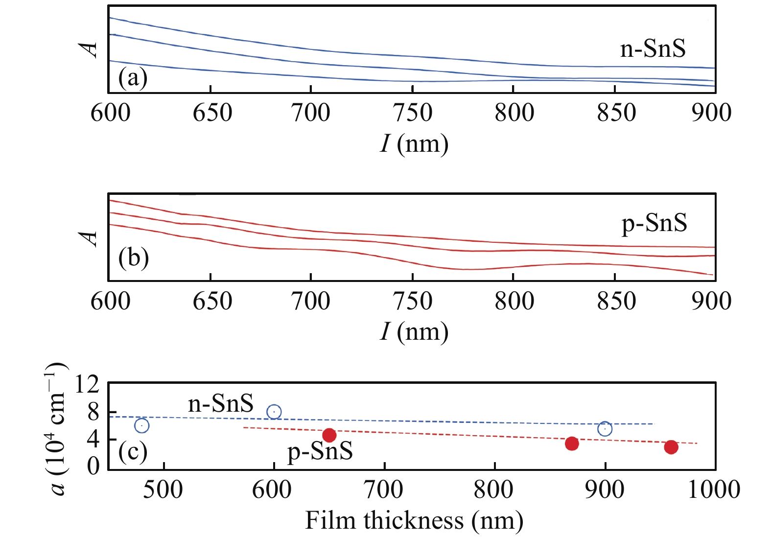
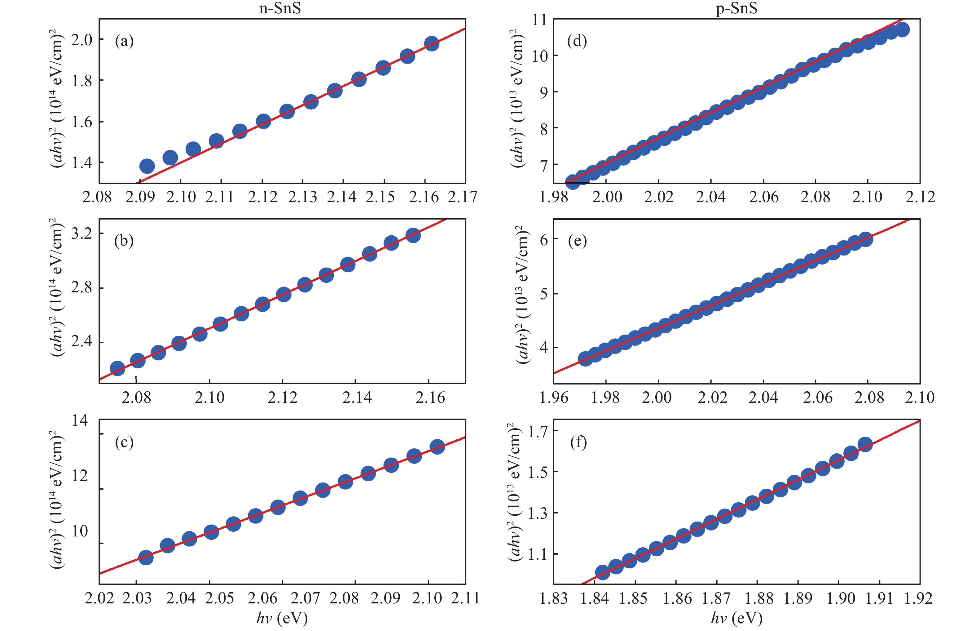
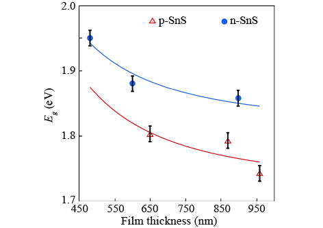
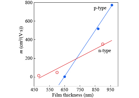
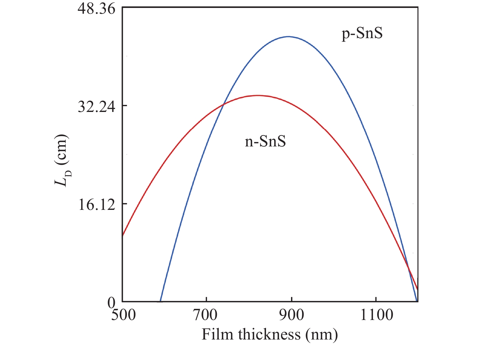
Abstract: This work presents a comparative study of n-SnS and p-SnS active layers for increased solar cell efficiency. Tin sulphide thin films of various thicknesses having p-type and n-type conductivity were fabricated by thermal evaporation. Both type of films had the same (113) orientation of the crystal planes with a constant tensile strain of ~ 0.003 and ~ 0.011, respectively. The persistent photocurrent was observed in all n-SnS and p-SnS samples with the current’s time decay constant decreasing with increasing film thickness. Hole mobility of thicker p-SnS films was found to be greater than the electron mobility in n-SnS samples, with mobility (both hole and electron) showing an increasing trend with film thickness. The optimum absorber layer thickness for both p- and n-SnS layers should have a high value of diffusion length for a given absorption coefficient and band-gap.
Keywords: thin film, chalcogenides, optical properties
| [1] |
Dong Q, Fang Y, Shao Y, et al. Electron-hole diffusion lengths > 175 μm in solution-grown CH3NH3PbI3 single crystals. Science, 2015, 347: 6225
|
| [2] |
Gao C, Shen H, Sun L. Preparation and properties of zinc blende and orthorhombic SnS films by chemical bath deposition. Appl Surf Sci, 2011, 257: 6750 doi: 10.1016/j.apsusc.2011.02.116
|
| [3] |
Sohila S, Rajalakshmi M, Ghosh C, et al. Optical and Raman Scattering studies on SnS nano-particles. J Alloys Compd, 2011, 509: 5843 doi: 10.1016/j.jallcom.2011.02.141
|
| [4] |
Fadavieslam M R, Shahtahmasebi N, Razaee-Roknabadi M, et al. A study of the photoconductivity and thermoelectric properties of SnxSy optical semiconductor thin films deposited by the spray pyrolysis technique. Phys Scr, 2011, 84: 035705 doi: 10.1088/0031-8949/84/03/035705
|
| [5] |
Gomez A, Martinez H, Calixto-Rodriguez M, et al. A study of the structural, optical and electrical properties of SnS thin films modified by plasma. J Mater Sci Eng B, 2013, 3: 352
|
| [6] |
Ogah O E, Reddy K R, Zoppi G, et al. Annealing studies and electrical properties of SnS-based solar cells. Thin Solid Films, 2011, 519: 7425 doi: 10.1016/j.tsf.2010.12.235
|
| [7] |
Leach M, Reddy K T R, Reddy M V, et al. Tin sulphide thin films synthesised using a two step process. Energy Procedia, 2012, 15: 371 doi: 10.1016/j.egypro.2012.02.045
|
| [8] |
Ristov M, Sinadinovski G, Grozdanov J, et al. Chemical deposition of tin(II) sulphide thin films. Thin Solid Films, 1989, 173: 53 doi: 10.1016/0040-6090(89)90536-1
|
| [9] |
Sajeesh T H, Jinesh K B, Rao M, et al. Unveiling the defect levels in SnS thin films for photovoltaic applications using photoluminescence technique. Phys Status Solidi A, 2010, 207: 1934 doi: 10.1002/pssa.200925593
|
| [10] |
Sinsermsuksakul P, Heo J, Noh W, et al. Atomic layer deposition of tin monosulfide thin films. Adv Energy Mater, 2011, 7: 1116
|
| [11] |
Sinsermsuksakul P, Hartman K, Kim S B, et al. Enhancing the efficiency of SnS solar cells via band-offset engineering with a zinc oxysulfide buffer layer. Appl Phys Lett, 2013, 102: 053901 doi: 10.1063/1.4789855
|
| [12] |
Stavrinadis A, Smith J M, Cattley C A, et al. SnS/PbS nanocrystal hetrojunction photovoltaics. Nanotechnology, 2010, 21: 185202 doi: 10.1088/0957-4484/21/18/185202
|
| [13] |
Jain P, Arun P. Photovoltaic performance of hybrid ITO/PEDOT:PSS/n-SnS/Al solar cell structure. J Semicond, 2016, 37: 074002 doi: 10.1088/1674-4926/37/7/074002
|
| [14] |
Jain P, Shokeen P, Arun P. Improved efficiency of plasmonic tin sulfide solar cells. J Mater Sci: Mater Elec, 2016, 27: 5107 doi: 10.1007/s10854-016-4401-0
|
| [15] |
Gupta Y, Arun P. Suitability of SnS thin films for photovoltaic application due to the existence of persistent photocurrent. Phys Status Solidi B, 2016, 253: 509 doi: 10.1002/pssb.v253.3
|
| [16] |
Vidal J, Lany S, d’Avezac M, et al. Band-structure, optical properties, and defect physics of the photovoltaic semiconductor SnS. Appl Phys Lett, 2012, 100: 032104 doi: 10.1063/1.3675880
|
| [17] |
Ninan G G, Kartha C S, Vijayakumar K P et al. Spray pyrolysed SnS thin films in n and p type: optimization of deposition process and characterization of samples. J Analyt Appl Pyrolysis, 2016, 120: 121 doi: 10.1016/j.jaap.2016.04.016
|
| [18] |
Ran F Y, Xiao Z, Toda Y, et al. n-type conversion of SnS by isovalent ion substitution: geometrical doping as a new doping route. Sci Rep, 2015, 5: 10428 doi: 10.1038/srep10428
|
| [19] |
Chandrashekhar H R, Humphreys R G, Zwick U, et al. Infrared and Raman spectra of the IV–VI compounds SnS and SnSe. Phys Rev B, 1977, 15: 2177 doi: 10.1103/PhysRevB.15.2177
|
| [20] |
Alim K A, Fonoberrov V A, Baladdin A A. Origin of the optical phonon frequency shifts in ZnO quantum dots. Appl Phys Lett, 20015, 86: 053103
|
| [21] |
Zhu J S, Lu X M, Jiang W, et al. Optical study on the size effects in BaTiO3 thin films. J Appl Phys, 1997, 81: 1392 doi: 10.1063/1.363875
|
| [22] |
Rajalakshmi M, Arora A K, Bendre B S, et al. Optical phonon confinement in zinc oxide nanoparticles. J Appl Phys, 2000, 87: 2445 doi: 10.1063/1.372199
|
| [23] |
Lucovsky G, Mikkelsen J C, Liang W Y, et al. Optical phonon anisotropies in the layer crystals SnS2 and SnSe2. Phys Rev B, 1976, 14: 1663 doi: 10.1103/PhysRevB.14.1663
|
| [24] |
Dang X Z, Wang C D, Yu E T, et al. Persistent photoconductivity and defect levels in n-type AlGaN/GaN hetrostructures. Appl Phys Lett, 1998, 72: 2745 doi: 10.1063/1.121077
|
| [25] |
Gupta Y, Arun P. Influence of Urbach tail on the refractive index of p-SnS thin films. Phys Status Solidi C, 2017, 14: 1600207
|
| [26] |
Tauc J. Absorption edge and internal electric fields in amorphous semiconductors. Mater Res Bull, 1970, 5: 721 doi: 10.1016/0025-5408(70)90112-1
|
| [27] |
Brus L E. Electron–electron and electron–hole interactions in small semiconductor crystallites: the size dependence of the lowest excited electronic state. J Chem Phys, 1984, 80: 4403 doi: 10.1063/1.447218
|
| [28] |
Sze S M. Physics of semiconductor devices. 2nd ed. John Wiley and Sons, Inc. 1981
|
| [29] |
Ran F Y, Xiao Z, Toda Y, et al. n-type conversion of SnS by isovalent ion substitution: Geometrical doping as a new doping route. Sci Rep, 2015, 5: 10428 doi: 10.1038/srep10428
|
| [30] |
Gupta Y, Arun P. Influence of strain on the sensitivity of tin sulphide films. Mater Chem Phys, 2017, 191: 86 doi: 10.1016/j.matchemphys.2017.01.029
|


Article views: 4352 Times PDF downloads: 52 Times Cited by: 0 Times
Received: 11 February 2017 Revised: 13 April 2017 Online: Uncorrected proof: 30 October 2017Accepted Manuscript: 13 November 2017Published: 01 November 2017
| Citation: |
Yashika Gupta, P. Arun. Optimization of SnS active layer thickness for solar cell application[J]. Journal of Semiconductors, 2017, 38(11): 113001. doi: 10.1088/1674-4926/38/11/113001
****
Y Gupta, P. Arun. Optimization of SnS active layer thickness for solar cell application[J]. J. Semicond., 2017, 38(11): 113001. doi: 10.1088/1674-4926/38/11/113001.

|
| [1] |
Dong Q, Fang Y, Shao Y, et al. Electron-hole diffusion lengths > 175 μm in solution-grown CH3NH3PbI3 single crystals. Science, 2015, 347: 6225
|
| [2] |
Gao C, Shen H, Sun L. Preparation and properties of zinc blende and orthorhombic SnS films by chemical bath deposition. Appl Surf Sci, 2011, 257: 6750 doi: 10.1016/j.apsusc.2011.02.116
|
| [3] |
Sohila S, Rajalakshmi M, Ghosh C, et al. Optical and Raman Scattering studies on SnS nano-particles. J Alloys Compd, 2011, 509: 5843 doi: 10.1016/j.jallcom.2011.02.141
|
| [4] |
Fadavieslam M R, Shahtahmasebi N, Razaee-Roknabadi M, et al. A study of the photoconductivity and thermoelectric properties of SnxSy optical semiconductor thin films deposited by the spray pyrolysis technique. Phys Scr, 2011, 84: 035705 doi: 10.1088/0031-8949/84/03/035705
|
| [5] |
Gomez A, Martinez H, Calixto-Rodriguez M, et al. A study of the structural, optical and electrical properties of SnS thin films modified by plasma. J Mater Sci Eng B, 2013, 3: 352
|
| [6] |
Ogah O E, Reddy K R, Zoppi G, et al. Annealing studies and electrical properties of SnS-based solar cells. Thin Solid Films, 2011, 519: 7425 doi: 10.1016/j.tsf.2010.12.235
|
| [7] |
Leach M, Reddy K T R, Reddy M V, et al. Tin sulphide thin films synthesised using a two step process. Energy Procedia, 2012, 15: 371 doi: 10.1016/j.egypro.2012.02.045
|
| [8] |
Ristov M, Sinadinovski G, Grozdanov J, et al. Chemical deposition of tin(II) sulphide thin films. Thin Solid Films, 1989, 173: 53 doi: 10.1016/0040-6090(89)90536-1
|
| [9] |
Sajeesh T H, Jinesh K B, Rao M, et al. Unveiling the defect levels in SnS thin films for photovoltaic applications using photoluminescence technique. Phys Status Solidi A, 2010, 207: 1934 doi: 10.1002/pssa.200925593
|
| [10] |
Sinsermsuksakul P, Heo J, Noh W, et al. Atomic layer deposition of tin monosulfide thin films. Adv Energy Mater, 2011, 7: 1116
|
| [11] |
Sinsermsuksakul P, Hartman K, Kim S B, et al. Enhancing the efficiency of SnS solar cells via band-offset engineering with a zinc oxysulfide buffer layer. Appl Phys Lett, 2013, 102: 053901 doi: 10.1063/1.4789855
|
| [12] |
Stavrinadis A, Smith J M, Cattley C A, et al. SnS/PbS nanocrystal hetrojunction photovoltaics. Nanotechnology, 2010, 21: 185202 doi: 10.1088/0957-4484/21/18/185202
|
| [13] |
Jain P, Arun P. Photovoltaic performance of hybrid ITO/PEDOT:PSS/n-SnS/Al solar cell structure. J Semicond, 2016, 37: 074002 doi: 10.1088/1674-4926/37/7/074002
|
| [14] |
Jain P, Shokeen P, Arun P. Improved efficiency of plasmonic tin sulfide solar cells. J Mater Sci: Mater Elec, 2016, 27: 5107 doi: 10.1007/s10854-016-4401-0
|
| [15] |
Gupta Y, Arun P. Suitability of SnS thin films for photovoltaic application due to the existence of persistent photocurrent. Phys Status Solidi B, 2016, 253: 509 doi: 10.1002/pssb.v253.3
|
| [16] |
Vidal J, Lany S, d’Avezac M, et al. Band-structure, optical properties, and defect physics of the photovoltaic semiconductor SnS. Appl Phys Lett, 2012, 100: 032104 doi: 10.1063/1.3675880
|
| [17] |
Ninan G G, Kartha C S, Vijayakumar K P et al. Spray pyrolysed SnS thin films in n and p type: optimization of deposition process and characterization of samples. J Analyt Appl Pyrolysis, 2016, 120: 121 doi: 10.1016/j.jaap.2016.04.016
|
| [18] |
Ran F Y, Xiao Z, Toda Y, et al. n-type conversion of SnS by isovalent ion substitution: geometrical doping as a new doping route. Sci Rep, 2015, 5: 10428 doi: 10.1038/srep10428
|
| [19] |
Chandrashekhar H R, Humphreys R G, Zwick U, et al. Infrared and Raman spectra of the IV–VI compounds SnS and SnSe. Phys Rev B, 1977, 15: 2177 doi: 10.1103/PhysRevB.15.2177
|
| [20] |
Alim K A, Fonoberrov V A, Baladdin A A. Origin of the optical phonon frequency shifts in ZnO quantum dots. Appl Phys Lett, 20015, 86: 053103
|
| [21] |
Zhu J S, Lu X M, Jiang W, et al. Optical study on the size effects in BaTiO3 thin films. J Appl Phys, 1997, 81: 1392 doi: 10.1063/1.363875
|
| [22] |
Rajalakshmi M, Arora A K, Bendre B S, et al. Optical phonon confinement in zinc oxide nanoparticles. J Appl Phys, 2000, 87: 2445 doi: 10.1063/1.372199
|
| [23] |
Lucovsky G, Mikkelsen J C, Liang W Y, et al. Optical phonon anisotropies in the layer crystals SnS2 and SnSe2. Phys Rev B, 1976, 14: 1663 doi: 10.1103/PhysRevB.14.1663
|
| [24] |
Dang X Z, Wang C D, Yu E T, et al. Persistent photoconductivity and defect levels in n-type AlGaN/GaN hetrostructures. Appl Phys Lett, 1998, 72: 2745 doi: 10.1063/1.121077
|
| [25] |
Gupta Y, Arun P. Influence of Urbach tail on the refractive index of p-SnS thin films. Phys Status Solidi C, 2017, 14: 1600207
|
| [26] |
Tauc J. Absorption edge and internal electric fields in amorphous semiconductors. Mater Res Bull, 1970, 5: 721 doi: 10.1016/0025-5408(70)90112-1
|
| [27] |
Brus L E. Electron–electron and electron–hole interactions in small semiconductor crystallites: the size dependence of the lowest excited electronic state. J Chem Phys, 1984, 80: 4403 doi: 10.1063/1.447218
|
| [28] |
Sze S M. Physics of semiconductor devices. 2nd ed. John Wiley and Sons, Inc. 1981
|
| [29] |
Ran F Y, Xiao Z, Toda Y, et al. n-type conversion of SnS by isovalent ion substitution: Geometrical doping as a new doping route. Sci Rep, 2015, 5: 10428 doi: 10.1038/srep10428
|
| [30] |
Gupta Y, Arun P. Influence of strain on the sensitivity of tin sulphide films. Mater Chem Phys, 2017, 191: 86 doi: 10.1016/j.matchemphys.2017.01.029
|

 WeChat ID
Journal of Semiconductors © 2017 All Rights Reserved 京ICP备05085259号-2

 DownLoad:

