


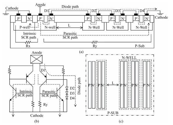
Fig. 1.
(a) The cross-section, (b) equivalent circuit, (c) and layout top view of the modified DTSCR structure with a large space between the trigger diodes D1 and D2.
SEMICONDUCTOR INTEGRATED CIRCUITS
Lizhong Zhang, Yuan Wang, Yize Wang and Yandong He
Corresponding author: Yuan Wang, E-mail:wangyuan@pku.edu.cn; Yandong He, E-mail:heyd@pku.edu.cn
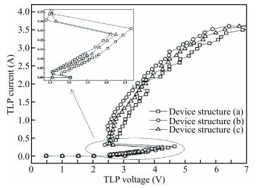
Abstract: The diode-triggered silicon-controlled rectifier (DTSCR) is widely used for electrostatic discharge (ESD) protection in advanced CMOS process owing to its advantages, such as design simplification, adjustable trigger/holding voltage, low parasitic capacitance. However, the multiple-triggering effect in the typical DTSCR device may cause undesirable larger overall trigger voltage, which results in a reduced ESD safe margin. In previous research, the major cause is attributed to the higher current level required in the intrinsic SCR. The related discussions indicate that it seems to result from the current division rule between the intrinsic and parasitic SCR formed in the triggering process. In this letter, inserting a large space into the trigger diodes is proposed to get a deeper insight into this issue. The triggering current is observed to be regularly reduced along with the increased space, which confirms that the current division is determined by the parasitic resistance distributed between the intrinsic and parasitic SCR paths. The theoretical analysis is well confirmed by device simulation and transmission line pulse (TLP) test results. The reduced overall trigger voltage is achieved in the modified DTSCR structures due to the comprehensive result of the parasitic resistance vs triggering current, which indicates a minimized multiple-triggering effect.
Keywords: electrostatic discharge (ESD), diode-triggered silicon-controlled rectifier (DTSCR), double snapback, transmission line pulse (TLP) test
| [1] |
Liao C J, Liu J Z, Liu Z W. A novel HBT trigger SCR in 0.35 μm SiGe BiCMOS technology. J Semicond, 2016, 37(9): 094004 doi: 10.1088/1674-4926/37/9/094004
|
| [2] |
Chen W Y, RosenBaum E, Ker M D. Diode-triggered silicon-controlled rectifier with reduced voltage overshoot for CDM ESD Protection. IEEE Trans Device Mater Rel, 2012, 12(1):10 doi: 10.1109/TDMR.2011.2171487
|
| [3] |
Liu J Z, Liu Z W, Jia Z, et al. A novel DTSCR with a variation lateral base doping structure to improve turn-on speed for ESD protection. J Semicond, 2014, 35(6): 064010 doi: 10.1088/1674-4926/35/6/064010
|
| [4] |
Zhang L Z, Wang Y, Lu G Y, et al. A novel diode string triggered gated-PiN junction device for electrostatic discharge protection in 65-nm CMOS technology. Chin Phys B, 2015, 24(10): 108503 doi: 10.1088/1674-1056/24/10/108503
|
| [5] |
Li J J, Sarro Di J, Li Y, et al. Investigation of SOI SCR triggering and current sustaining under DC and TLP conditions. Proc IEEE EOS/ESD Symp, 2013: 1 https://www.researchgate.net/publication/261446593_Investigation_of_SOI_SCR_triggering_and_current_sustaining_under_DC_and_TLP_conditions
|
| [6] |
Ginawi A, Xia T, Gauthier R. Reducing the turn-on time and overshoot voltage for a diode-triggered silicon-controlled rectifier during an electrostatic discharge event. Proc IEEE SOCC Symp, 2014: 1 https://www.researchgate.net/publication/287573967_Reducing_the_turn-on_time_and_overshoot_voltage_for_a_diode-triggered_silicon-controlled_rectifier_during_an_electrostatic_discharge_event
|
| [7] |
Mishra R, Li J J, Sarro Di J, et al. Effect of embedded-SiGe (eSiGe) on ESD TLP and VFTLP characteristics of diode-triggered silicon controlled rectifiers (DTSCRs). Proc IEEE EOS/ESD Symp, 2012 http://ieeexplore.ieee.org/xpl/abstractKeywords.jsp?reload=true&arnumber=6333323
|
| [8] |
Dong S R, Jin H, Miao M, et al. Novel capacitance coupling complementary dual-direction SCR for high-voltage. IEEE Electron Device Lett, 2012, 33(5): 640 doi: 10.1109/LED.2012.2188015
|
| [9] |
Bi X W, Liang H L, Gu X F, et al. Design of novel DDSCR with embedded PNP structure for ESD protection. J Semicond, 2015, 36(12): 124007 doi: 10.1088/1674-4926/36/12/124007
|
| [10] |
Lin C Y, Chu L W, Ker M D, et al. ESD protection structure with inductor-triggered SCR for RF applications in 65-nm CMOS process. Proc IEEE IRPS Symp, 2012: 1 https://www.infona.pl/resource/bwmeta1.element.ieee-art-000006241893
|
| [11] |
Sarro Di J, Chatty K, Gauthier R, et al. Evaluation of SCR-based ESD protection devices in 90 nm and 65 nm CMOS technologies. Proc IEEE IRPS Symp, 2007: 1 https://www.researchgate.net/publication/4252374_Evaluation_of_SCR-based_ESD_protection_devices_in_90nm_and_65nm_CMOS_technologies
|
| [12] |
Lin C Y, Wu P H, Ker M D. Area-efficient and low-leakage diode string for on-chip ESD protection. IEEE Trans Electron Devices, 2015, 63(2): 531 http://ieeexplore.ieee.org/document/7353163/citations
|
| [13] |
Zhang P, Wang Y, Jia S, et al. LDMOS-SCR: a replacement for LDMOS with high ESD self-protection ability for HV application. Semicond Sci Technol, 2012, 27(3): 035006 doi: 10.1088/0268-1242/27/3/035006
|
| [14] |
Wang Y, Lu G Y, Cao J, et al. Analysis of dummy-gate dual-directional SCR (dSCR) device for ESD protection. Proc IEEE IPFA Symp, 2013: 720 https://www.researchgate.net/publication/261195271_Analysis_of_dummy-gate_dual-directional_SCR_dSCR_device_for_ESD_protection
|
| [15] |
Miao M, Dong S R, Wu J, et al. Minimizing multiple triggering effect in diode-triggered silicon-controlled rectifiers for ESD protection applications. IEEE Electron Device Lett, 2012, 33(6): 893 doi: 10.1109/LED.2012.2191930
|
| [16] |
Shrivastava M, Schneider J, Jain R, et al. IGBT plugged in SCR device for ESD protection in advanced CMOS Technology. Proc, IEEE EOS/ESD Symp, 2009: 1 https://www.researchgate.net/publication/224084060_IGBT_plugged_in_SCR_device_for_ESD_protection_in_advanced_CMOS_technology
|


Article views: 3832 Times PDF downloads: 47 Times Cited by: 0 Times
Received: 06 December 2016 Revised: 12 January 2017 Online: Published: 01 July 2017
| Citation: |
Lizhong Zhang, Yuan Wang, Yize Wang, Yandong He. Insight into multiple-triggering effect in DTSCRs for ESD protection[J]. Journal of Semiconductors, 2017, 38(7): 075001. doi: 10.1088/1674-4926/38/7/075001
****
L Z Zhang, Y Wang, Y Z Wang, Yandong He and O N He. Insight into multiple-triggering effect in DTSCRs for ESD protection[J]. J. Semicond., 2017, 38(7): 075001. doi: 10.1088/1674-4926/38/7/075001.

|
| [1] |
Liao C J, Liu J Z, Liu Z W. A novel HBT trigger SCR in 0.35 μm SiGe BiCMOS technology. J Semicond, 2016, 37(9): 094004 doi: 10.1088/1674-4926/37/9/094004
|
| [2] |
Chen W Y, RosenBaum E, Ker M D. Diode-triggered silicon-controlled rectifier with reduced voltage overshoot for CDM ESD Protection. IEEE Trans Device Mater Rel, 2012, 12(1):10 doi: 10.1109/TDMR.2011.2171487
|
| [3] |
Liu J Z, Liu Z W, Jia Z, et al. A novel DTSCR with a variation lateral base doping structure to improve turn-on speed for ESD protection. J Semicond, 2014, 35(6): 064010 doi: 10.1088/1674-4926/35/6/064010
|
| [4] |
Zhang L Z, Wang Y, Lu G Y, et al. A novel diode string triggered gated-PiN junction device for electrostatic discharge protection in 65-nm CMOS technology. Chin Phys B, 2015, 24(10): 108503 doi: 10.1088/1674-1056/24/10/108503
|
| [5] |
Li J J, Sarro Di J, Li Y, et al. Investigation of SOI SCR triggering and current sustaining under DC and TLP conditions. Proc IEEE EOS/ESD Symp, 2013: 1 https://www.researchgate.net/publication/261446593_Investigation_of_SOI_SCR_triggering_and_current_sustaining_under_DC_and_TLP_conditions
|
| [6] |
Ginawi A, Xia T, Gauthier R. Reducing the turn-on time and overshoot voltage for a diode-triggered silicon-controlled rectifier during an electrostatic discharge event. Proc IEEE SOCC Symp, 2014: 1 https://www.researchgate.net/publication/287573967_Reducing_the_turn-on_time_and_overshoot_voltage_for_a_diode-triggered_silicon-controlled_rectifier_during_an_electrostatic_discharge_event
|
| [7] |
Mishra R, Li J J, Sarro Di J, et al. Effect of embedded-SiGe (eSiGe) on ESD TLP and VFTLP characteristics of diode-triggered silicon controlled rectifiers (DTSCRs). Proc IEEE EOS/ESD Symp, 2012 http://ieeexplore.ieee.org/xpl/abstractKeywords.jsp?reload=true&arnumber=6333323
|
| [8] |
Dong S R, Jin H, Miao M, et al. Novel capacitance coupling complementary dual-direction SCR for high-voltage. IEEE Electron Device Lett, 2012, 33(5): 640 doi: 10.1109/LED.2012.2188015
|
| [9] |
Bi X W, Liang H L, Gu X F, et al. Design of novel DDSCR with embedded PNP structure for ESD protection. J Semicond, 2015, 36(12): 124007 doi: 10.1088/1674-4926/36/12/124007
|
| [10] |
Lin C Y, Chu L W, Ker M D, et al. ESD protection structure with inductor-triggered SCR for RF applications in 65-nm CMOS process. Proc IEEE IRPS Symp, 2012: 1 https://www.infona.pl/resource/bwmeta1.element.ieee-art-000006241893
|
| [11] |
Sarro Di J, Chatty K, Gauthier R, et al. Evaluation of SCR-based ESD protection devices in 90 nm and 65 nm CMOS technologies. Proc IEEE IRPS Symp, 2007: 1 https://www.researchgate.net/publication/4252374_Evaluation_of_SCR-based_ESD_protection_devices_in_90nm_and_65nm_CMOS_technologies
|
| [12] |
Lin C Y, Wu P H, Ker M D. Area-efficient and low-leakage diode string for on-chip ESD protection. IEEE Trans Electron Devices, 2015, 63(2): 531 http://ieeexplore.ieee.org/document/7353163/citations
|
| [13] |
Zhang P, Wang Y, Jia S, et al. LDMOS-SCR: a replacement for LDMOS with high ESD self-protection ability for HV application. Semicond Sci Technol, 2012, 27(3): 035006 doi: 10.1088/0268-1242/27/3/035006
|
| [14] |
Wang Y, Lu G Y, Cao J, et al. Analysis of dummy-gate dual-directional SCR (dSCR) device for ESD protection. Proc IEEE IPFA Symp, 2013: 720 https://www.researchgate.net/publication/261195271_Analysis_of_dummy-gate_dual-directional_SCR_dSCR_device_for_ESD_protection
|
| [15] |
Miao M, Dong S R, Wu J, et al. Minimizing multiple triggering effect in diode-triggered silicon-controlled rectifiers for ESD protection applications. IEEE Electron Device Lett, 2012, 33(6): 893 doi: 10.1109/LED.2012.2191930
|
| [16] |
Shrivastava M, Schneider J, Jain R, et al. IGBT plugged in SCR device for ESD protection in advanced CMOS Technology. Proc, IEEE EOS/ESD Symp, 2009: 1 https://www.researchgate.net/publication/224084060_IGBT_plugged_in_SCR_device_for_ESD_protection_in_advanced_CMOS_technology
|

 WeChat ID
Journal of Semiconductors © 2017 All Rights Reserved 京ICP备05085259号-2

 DownLoad:

