SEMICONDUCTOR DEVICES

FEM thermal analysis of high power GaN-on-diamond HEMTs

Xudong Chen1, 2, Wenbo Zhai1, 2, Jingwen Zhang1, 2, 3, , Renan Bu2, Hongxing Wang2 and Xun Hou2

+ Author Affiliations

 Corresponding author: Jingwen Zhang, Email: jwzhang@xjtu.edu.cn

PDF

Turn off MathJax

Abstract: A three-dimensional thermal analysis of GaN HEMTs on diamond substrate is investigated using the finite element method. The diamond substrate thickness, area and shape, transition layer thickness and thermal conductivity of the transition layer are considered and treated appropriately in the numerical simulation. The temperature distribution and heat spreading paths are investigated under different conditions and the results indicate that the existence of the transition layer causes an increase in the channel temperature and the thickness, area and shape of the diamond substrate have certain impacts on the channel temperature too. Channel temperature reduces with increasing diamond substrate thickness and area but with a decreasing trend, which can be explained by the saturation effects of the diamond substrate. The shape of diamond substrate also affects the temperature performance of GaN HEMTs, therefore, to achieve a favorable heat dissipation effect with the settled diamond substrate area, the shape should contain as many isothermal curves as possible when the isothermal gradient is constant. The study of the thermal properties of GaN on diamond substrate is useful for the prediction of heating of high power GaN HEMTs devices and optimal designs of an efficient heat spreader for GaN HEMTs.

Key words: FEMGaN-on-diamond HEMTsself-heatingtemperature distribution


[1]
Jimenez J L, Chowdhury U. X-band GaN FET reliability. Proc IEEE IRPS, 2008: 429
[2]
Lee S, Vetury R, Brown J D, et al. Reliability assessment of AlGaN/GaN HEMT technology on SiC for 48 V applications. Proc IEEE 46th Annu Int Rel Phys Symp, 2008: 446
[3]
Singhal S, Roberts J C, Rajagopal P, et al. GaN-on-Si failure mechanisms and reliability improvements. Proc IEEE IRPS, 2006: 95
[4]
Kemerley R T, Wallace H B, Yoder M N. Impact of wide bandgap microwave devices on DoD systems. Proc IEEE, 2002, 90(6): 1059 doi: 10.1109/JPROC.2002.1021570
[5]
Mishra U K, Parikh P, Wu Y F. AlGaN/GaN HEMTs-an overview of device operation and applications. Proc IEEE, 2002, 90(11): 1022
[6]
Sullivan G J, Chen M Y, Higgins J A, et al. High-power 10-GHz operation of AlGaN HFET's on insulating SiC. IEEE Electron Device Lett, 1998, 19(6): 198 doi: 10.1109/55.678543
[7]
Trew R J. SiC and GaN transistors-is there one winner for microwave power applications. Proc IEEE, 2002, 90(6): 1032 doi: 10.1109/JPROC.2002.1021568
[8]
Menozzi R, Umana-Membreno G A, Nener B D, et al. Temperature-dependent characterization of AlGaN/GaN HEMTs: thermal and source/drain resistances. IEEE Trans Device Mater Rel, 2008, 8(2): 255 doi: 10.1109/TDMR.2008.918960
[9]
Bar-Cohen A, AlbrechtJ D, Maurer J J. Near-junction thermal mnagement for wide bandgap devices. Proc IEEE CSICS, 2011: 1
[10]
Meneghesso G, Verzellesi G, Danesin F, et al. Reliability of GaN high-electron-mobility transistors: state of the art and perspectives. IEEE Trans. Dev. Mat. Rel., 2008, 8(2): 332 doi: 10.1109/TDMR.2008.923743
[11]
Altman D, Tyhach M, Mcclymonds J, et al. Analysis and characterization of thermal transport in GaN HEMTs on Diamond substrates. Fourteenth Intersociety Conference on Thermal and Thermomechanical Phenomena in Electronic Systems, 2014: 1199
[12]
Pomeroy J, Bernardoni M, Sarua A, et al. Achieving the best thermal performance for GaN-on-diamond. Proc IEEE Compnd Semicondr Integr Circuit Symp (CSICS), 2013: 1
[13]
Ejeckam F, Francis D, Faili F, et al. S2-T1: GaN-on-diamond: A brief history. Proc IEEE Lester Eastman Conf High Perform. Devices, 2014: 1
[14]
Zhao M, Liu X, Zheng Y, et al. Thermal analysis of AlGaN/GaN high-electron-mobility transistors by infrared microscopy. Physical & Failure Analysis of Integrated Circuits, 2013, 291(12): 1
[15]
Hancock B L, Nazari M, Anderson J, et al. Ultraviolet micro-Raman spectroscopy stress mapping of a 75-mm GaN-on-diamond wafer. Appl Phys Lett, 2016, 108(21): 1467
[16]
Hancock B L, Nazari M, Anderson J, et al. Investigation of stresses in GaN HEMT layers on a diamond substrate using micro-raman spectroscopy. Compound Semiconductor Integrated Circuit Symposium, 2016: 1
[17]
Pomeroy J W, Bernardoni M, Dumka D C, et al. Low thermal resistance GaN-on-diamond transistors characterized by three-dimensional Raman thermography mapping. Appl Phys Lett, 2014, 104(8): 083513 doi: 10.1063/1.4865583
[18]
Sun H, Simon R B, Pomeroy J W, et al. Reducing GaN-on-diamond interfacial thermal resistance for high power transistor applications. Appl Phys Lett, 2015, 106(11): 229
[19]
Calame J P, Myers R E, Wood F N, et al. Simulations of direct-die-attached microchannel coolers for the thermal management of GaN-on-SiC microwave amplifiers. IEEE Trans Compon Pack Technol, 2005, 28(4): 797 doi: 10.1109/TCAPT.2005.848584
[20]
Bertoluzza F, Delmonte N, Menozzi R. Three-dimensional finite-element thermal simulation of GaN-based HEMTs. Microelectron Reliab, 2009, 49(5): 468 doi: 10.1016/j.microrel.2009.02.009
[21]
Chu K K, Yurovchak T, Chao P C, et al. Thermal modeling of high power GaN-on-diamond HEMTs fabricated by low-temperature device transfer process. Compound Semiconductor Integrated Circuit Symposium, 2013: 1
[22]
Wang A, Tadjer M J, Calle F. Simulation of thermal management in AlGaN/GaN HEMTs with integrated diamond heat spreaders. Semicond Sci Technol, 2013, 28(5): 055010 doi: 10.1088/0268-1242/28/5/055010
[23]
Denu G A, Mirani J H, Fu J, et al. FEM thermal analysis of Cu/diamond/Cu and diamond/SiC heat spreaders. AIP Adv, 2017, 7(3): 035102 doi: 10.1063/1.4978043
[24]
Liu T, Kong Y, Wu L, et al. 3-inch GaN-on-diamond HEMTs with device-first transfer technology. IEEE Electron Device Lett, 2017, 37: 1417
Fig. 1.  (Color online) Schematic diagram of GaN HEMTs. (a) Cross section of GaN HEMTs. (b) Top view of GaN HEMTs. (c) Partial enlarged drawing of GaN HEMTs.

Fig. 2.  (Color online) Temperature distribution of (a) the overall module, (b) diamond and GaN, (c) GaN surface, and (d) a specific finger.

Fig. 3.  (Color online) Cross section of temperature distribution. (a) The overall module. (b) The channel in the middle. (c) The channel near the edge.

Fig. 4.  (Color online) Temperature distribution along the horizontal position of the diamond substrate for variable diamond thickness.

Fig. 5.  (Color online) Temperature distribution along the vertical position of the diamond for different diamond thickness.

Fig. 6.  (Color online) Dependence of maximum temperature on the area ratio of diamond and GaN.

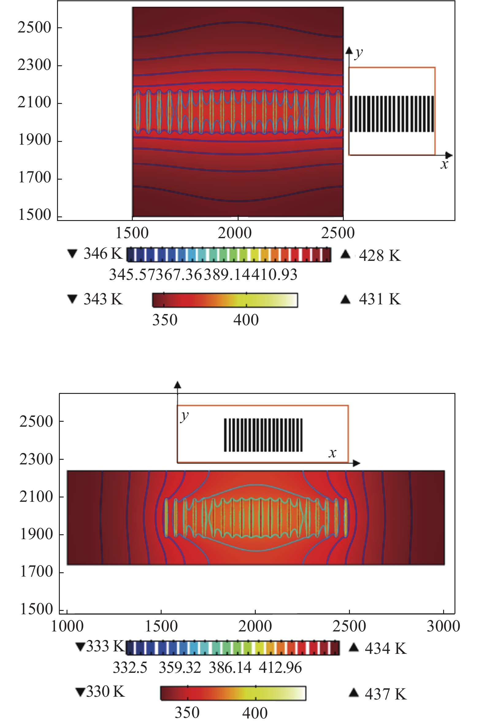
Fig. 7.  (Color online) Isothermal planforms based on two different diamond shapes. (a) 1000 × 1000 μm2. (b) 2000 × 500 μm2.

Fig. 8.  (Color online) Temperature distribution along the horizontal position of GaN for different diamond shapes.

Fig. 9.  (Color online) An ideal temperature distribution diagram.

Fig. 10.  (Color online) Dependence of maximum temperature on thermal conductivity and thickness of transition layer.

Table 1.   Geometric parameters of GaN MMIC.

Symbol Definition Value
lCu Length of Cu 4 mm
wCu Width of Cu 4 mm
hCu Thickness of Cu 2 mm
ldiamond Length of diamond 2 mm
wdiamond Width of diamond 1 mm
hdiamond Thickness of diamond 60–160 μm
hAuSn Thickness of AuSn 20 μm
h1 Thickness of transition layer 100–500 nm
hGaN Thickness of GaN layer 1.2–2.4 μm
hg Thickness of gate 0.3 μm
ld Gate to gate 50 μm
lg Length of gate 0.5 μm
hAlGaN Thickness of AlGaN 22 nm
DownLoad: CSV

Table 2.   Material properties used in simulation.

Material k(W/(m·K)) ρ (kg/m3) Cp (J/(kg·K))
GaN 130 6070 490
Cu 401 8960 384
Diamond 1800 3515 516
AuSn 57 14700 128
AlGaN 25 6070 490
DownLoad: CSV

Table 3.   Increase the area of diamond with Method 1.

Diamond area (μm2) Area ratio Maximum temperature (K) Diamond area (μm2) Area ratio Maximum temperature (K)
1000 × 200 1 565 2000 × 600 6 456
1000 × 400 2 492 2000 × 700 7 451
1000 × 600 3 470 2000 × 800 8 449
1000 × 800 4 461 2000 × 900 9 445
1000 × 1000 5 457 2000 × 1000 10 444
DownLoad: CSV
[1]
Jimenez J L, Chowdhury U. X-band GaN FET reliability. Proc IEEE IRPS, 2008: 429
[2]
Lee S, Vetury R, Brown J D, et al. Reliability assessment of AlGaN/GaN HEMT technology on SiC for 48 V applications. Proc IEEE 46th Annu Int Rel Phys Symp, 2008: 446
[3]
Singhal S, Roberts J C, Rajagopal P, et al. GaN-on-Si failure mechanisms and reliability improvements. Proc IEEE IRPS, 2006: 95
[4]
Kemerley R T, Wallace H B, Yoder M N. Impact of wide bandgap microwave devices on DoD systems. Proc IEEE, 2002, 90(6): 1059 doi: 10.1109/JPROC.2002.1021570
[5]
Mishra U K, Parikh P, Wu Y F. AlGaN/GaN HEMTs-an overview of device operation and applications. Proc IEEE, 2002, 90(11): 1022
[6]
Sullivan G J, Chen M Y, Higgins J A, et al. High-power 10-GHz operation of AlGaN HFET's on insulating SiC. IEEE Electron Device Lett, 1998, 19(6): 198 doi: 10.1109/55.678543
[7]
Trew R J. SiC and GaN transistors-is there one winner for microwave power applications. Proc IEEE, 2002, 90(6): 1032 doi: 10.1109/JPROC.2002.1021568
[8]
Menozzi R, Umana-Membreno G A, Nener B D, et al. Temperature-dependent characterization of AlGaN/GaN HEMTs: thermal and source/drain resistances. IEEE Trans Device Mater Rel, 2008, 8(2): 255 doi: 10.1109/TDMR.2008.918960
[9]
Bar-Cohen A, AlbrechtJ D, Maurer J J. Near-junction thermal mnagement for wide bandgap devices. Proc IEEE CSICS, 2011: 1
[10]
Meneghesso G, Verzellesi G, Danesin F, et al. Reliability of GaN high-electron-mobility transistors: state of the art and perspectives. IEEE Trans. Dev. Mat. Rel., 2008, 8(2): 332 doi: 10.1109/TDMR.2008.923743
[11]
Altman D, Tyhach M, Mcclymonds J, et al. Analysis and characterization of thermal transport in GaN HEMTs on Diamond substrates. Fourteenth Intersociety Conference on Thermal and Thermomechanical Phenomena in Electronic Systems, 2014: 1199
[12]
Pomeroy J, Bernardoni M, Sarua A, et al. Achieving the best thermal performance for GaN-on-diamond. Proc IEEE Compnd Semicondr Integr Circuit Symp (CSICS), 2013: 1
[13]
Ejeckam F, Francis D, Faili F, et al. S2-T1: GaN-on-diamond: A brief history. Proc IEEE Lester Eastman Conf High Perform. Devices, 2014: 1
[14]
Zhao M, Liu X, Zheng Y, et al. Thermal analysis of AlGaN/GaN high-electron-mobility transistors by infrared microscopy. Physical & Failure Analysis of Integrated Circuits, 2013, 291(12): 1
[15]
Hancock B L, Nazari M, Anderson J, et al. Ultraviolet micro-Raman spectroscopy stress mapping of a 75-mm GaN-on-diamond wafer. Appl Phys Lett, 2016, 108(21): 1467
[16]
Hancock B L, Nazari M, Anderson J, et al. Investigation of stresses in GaN HEMT layers on a diamond substrate using micro-raman spectroscopy. Compound Semiconductor Integrated Circuit Symposium, 2016: 1
[17]
Pomeroy J W, Bernardoni M, Dumka D C, et al. Low thermal resistance GaN-on-diamond transistors characterized by three-dimensional Raman thermography mapping. Appl Phys Lett, 2014, 104(8): 083513 doi: 10.1063/1.4865583
[18]
Sun H, Simon R B, Pomeroy J W, et al. Reducing GaN-on-diamond interfacial thermal resistance for high power transistor applications. Appl Phys Lett, 2015, 106(11): 229
[19]
Calame J P, Myers R E, Wood F N, et al. Simulations of direct-die-attached microchannel coolers for the thermal management of GaN-on-SiC microwave amplifiers. IEEE Trans Compon Pack Technol, 2005, 28(4): 797 doi: 10.1109/TCAPT.2005.848584
[20]
Bertoluzza F, Delmonte N, Menozzi R. Three-dimensional finite-element thermal simulation of GaN-based HEMTs. Microelectron Reliab, 2009, 49(5): 468 doi: 10.1016/j.microrel.2009.02.009
[21]
Chu K K, Yurovchak T, Chao P C, et al. Thermal modeling of high power GaN-on-diamond HEMTs fabricated by low-temperature device transfer process. Compound Semiconductor Integrated Circuit Symposium, 2013: 1
[22]
Wang A, Tadjer M J, Calle F. Simulation of thermal management in AlGaN/GaN HEMTs with integrated diamond heat spreaders. Semicond Sci Technol, 2013, 28(5): 055010 doi: 10.1088/0268-1242/28/5/055010
[23]
Denu G A, Mirani J H, Fu J, et al. FEM thermal analysis of Cu/diamond/Cu and diamond/SiC heat spreaders. AIP Adv, 2017, 7(3): 035102 doi: 10.1063/1.4978043
[24]
Liu T, Kong Y, Wu L, et al. 3-inch GaN-on-diamond HEMTs with device-first transfer technology. IEEE Electron Device Lett, 2017, 37: 1417
  • Search

    Advanced Search >>

    GET CITATION

    shu

    Export: BibTex EndNote

    Article Metrics

    Article views: 4320 Times PDF downloads: 100 Times Cited by: 0 Times

    History

    Received: 28 February 2018 Revised: 23 April 2018 Online: Uncorrected proof: 28 May 2018Published: 09 October 2018

    Catalog

      Email This Article

      User name:
      Email:*请输入正确邮箱
      Code:*验证码错误
      Xudong Chen, Wenbo Zhai, Jingwen Zhang, Renan Bu, Hongxing Wang, Xun Hou. FEM thermal analysis of high power GaN-on-diamond HEMTs[J]. Journal of Semiconductors, 2018, 39(10): 104005. doi: 10.1088/1674-4926/39/10/104005 ****X D Chen, W B Zhai, J W Zhang, R N Bu, H X Wang, X Hou, FEM thermal analysis of high power GaN-on-diamond HEMTs[J]. J. Semicond., 2018, 39(10): 104005. doi: 10.1088/1674-4926/39/10/104005.
      Citation:
      Xudong Chen, Wenbo Zhai, Jingwen Zhang, Renan Bu, Hongxing Wang, Xun Hou. FEM thermal analysis of high power GaN-on-diamond HEMTs[J]. Journal of Semiconductors, 2018, 39(10): 104005. doi: 10.1088/1674-4926/39/10/104005 ****
      X D Chen, W B Zhai, J W Zhang, R N Bu, H X Wang, X Hou, FEM thermal analysis of high power GaN-on-diamond HEMTs[J]. J. Semicond., 2018, 39(10): 104005. doi: 10.1088/1674-4926/39/10/104005.

      FEM thermal analysis of high power GaN-on-diamond HEMTs

      doi: 10.1088/1674-4926/39/10/104005
      Funds:

      Project supported by the National Natural Science Foundation of China (Nos. 60876042, 61176018, 61627812).

      More Information
      • Corresponding author: Email: jwzhang@xjtu.edu.cn
      • Received Date: 2018-02-28
      • Revised Date: 2018-04-23
      • Published Date: 2018-10-01

      Catalog

        /

        DownLoad:  Full-Size Img  PowerPoint
        Return
        Return