SEMICONDUCTOR MATERIALS

Implementation of slow and smooth etching of GaN by inductively coupled plasma

Xilin Li1, 2, 3, Ping Ma1, 2, 3, Xiaoli Ji1, 2, 3, Tongbo Wei1, 2, 3, , Xiaoyu Tan1, 2, 3, Junxi Wang1, 2, 3 and Jinmin Li1, 2, 3

+ Author Affiliations

 Corresponding author: Tongbo Wei, tbwei@semi.ac.cn

PDF

Turn off MathJax

Abstract: Slow and smooth etching of gallium nitride (GaN) by BCl3/Cl2-based inductively coupled plasma (ICP) is investigated in this paper. The effects of etch parameters, including ICP power, radio frequency (RF) power, the flow rate of Cl2 and BCl3, on GaN etch rate and etch surface roughness RMS are discussed. A new model is suggested to explain the impact mechanism of the BCl3 flow rate on etch surface roughness. An optimized etch result of a slow and smooth etch surface was obtained; the etch rate and RMS were 0.36 Å/s and 0.9 nm, respectively.

Key words: GaNICPslow etchingsmooth etching


[1]
Cordier Y, Semonda F, Lorenzini P, et al. MBE growth of AlGaN/GaN HEMTs on resistive Si(111) substrate with RF small signal and power performances. J Cryst Growth, 2003, 251(1): 811 doi: 10.1109/MBE.2002.1037778
[2]
Li G Q, Shih S J, Fu Z Y, et al. A new system for synthesis of high quality nonpolar GaN thin films. Chem Commun, 2010, 46(8): 1206 doi: 10.1039/B919722B
[3]
Li G Q, Wang W L, Yang W J, et al. Epitaxial growth of group III-nitride films by pulsed laser deposition and their use in the development of LED devices. Surf Sci Rep, 2015, 70: 380 doi: 10.1016/j.surfrep.2015.06.001
[4]
Yang W J, Wang W L, Lin Y H, et al. Deposition of nonpolar m-plane InGaN/GaN multiple quantum wells on LiGaO2(100) substrates. J Mater Chem C, 2014, 2: 801 doi: 10.1039/C3TC31935K
[5]
Li G Q, Wang W L, Yang W J, et al. GaN-based light-emitting diodes on various substrates: a critical review. Rep Prog Phys, 2016, 79: 45 doi: 0.1088/0034-4885/79/5/056501
[6]
Storm D F, Katzer D S, Roussos J A, et al. AlGaN/GaN HEMTs on free-standing GaN substrates: MBE growth and microwave characterization. J Cryst Growth, 2007, 301: 429 doi: doi.org/10.1016/j.jcrysgro.2006.11.085
[7]
Adesida I, Youtsey C, Ping A T. Dry and wet etching for group III–nitrides. MRS Proc, 1998: 537 doi: doi.org/10.1557/PROC-537-G1.4
[8]
Luo Y, Han Y J, Wu T, et al. Inductively coupled plasma etching of GaN-based materials. First Asia-Pacific Workshop on Wide Bandgap Semiconductors, 2003: 210
[9]
Qiu R F, Lu H, Chen D J, et al. Optimization of inductively coupled plasma deep etching of GaN and etching damage analysis. Appl Surf Sci, 2011, 257(15): 2700 doi: doi.org/10.1016/j.apsusc.2010.10.048
[10]
Shul R J, McClellan G B, Casalnuovo S A, et al. Inductively coupled plasma etching of GaN. Appl Phys Lett, 1996, 69(8): 1119 doi: 10.1063/1.117077
[11]
Cao X A, Zhang A P, Dang G T, et al. Schottky diode measurements of dry etch damage in n- and p-type GaN. J Vac Sci Technol, 2000, 18(4): 1144 doi: 10.1116/1.582314
[12]
Pearton S J, Lee J W, Mackenzie J D, et al. dry etch damage in InN, InGaN, and InAlN. Appl Phys Lett, 1995, 67(16): 2329 doi: 10.1063/1.114334
[13]
Cao X A, Cho H, Pearton S J, et al. Depth and thermal stability of dry etch damage in GaN Schottky diodes. Appl Phys Lett, 1999, 75(2): 232 doi: 10.1063/1.124332
[14]
Shul R J, Zhang L, Baca A G, et al. Inductively coupled plasma-induced etch damage of GaN p–n junctions. J Vac Sci Technol A, 2000, 18(4): 1139 doi: 10.1116/1.582313
[15]
Zhou S J, Cao B, Liu S. Dry etching characteristics of GaN using Cl2/BCl3 inductively coupled plasmas. Appl Surf Sci, 2010, 257: 905 doi: 10.1016/j.apsusc.2010.07.088
[16]
Rawal D S, Sehgal B K, Muralidharan R, et al. Effect of BCl3 concentration and process pressure on the GaN mesa sidewalls in BCl3/Cl2 based inductively coupled plasma etching. Vacuum, 2012, 86: 1844 doi: 10.1016/j.vacuum.2012.04.018
[17]
Wang W, Cai Y, Zhang B S, et al. The control of ICP etching GaN sidewall profiles and etch rate. Res Prog SSE, 2012, 32(3): 219
[18]
Wakejima A, Ando A, Watanabe A, et al. Normally off AlGaN/GaN HEMT on Si substrate with selectively dry etched recessed gate and polarization charge compensation δ-doped GaN cap layer. Appl Phys Express, 2015, 8(2): 37 doi: dx.doi.org/10.7567/APEX.8.026502
[19]
Arulkumaran S, Egaway T, Selvaraj L, et al. On the effects of gate-recess etching in current-collapse of different cap layers grown AlGaN/GaN high-electron-mobility transistors. Jpn J Appl Phys, 2006, 45(8): L220 doi: 10.1143/JJAP.45.L220
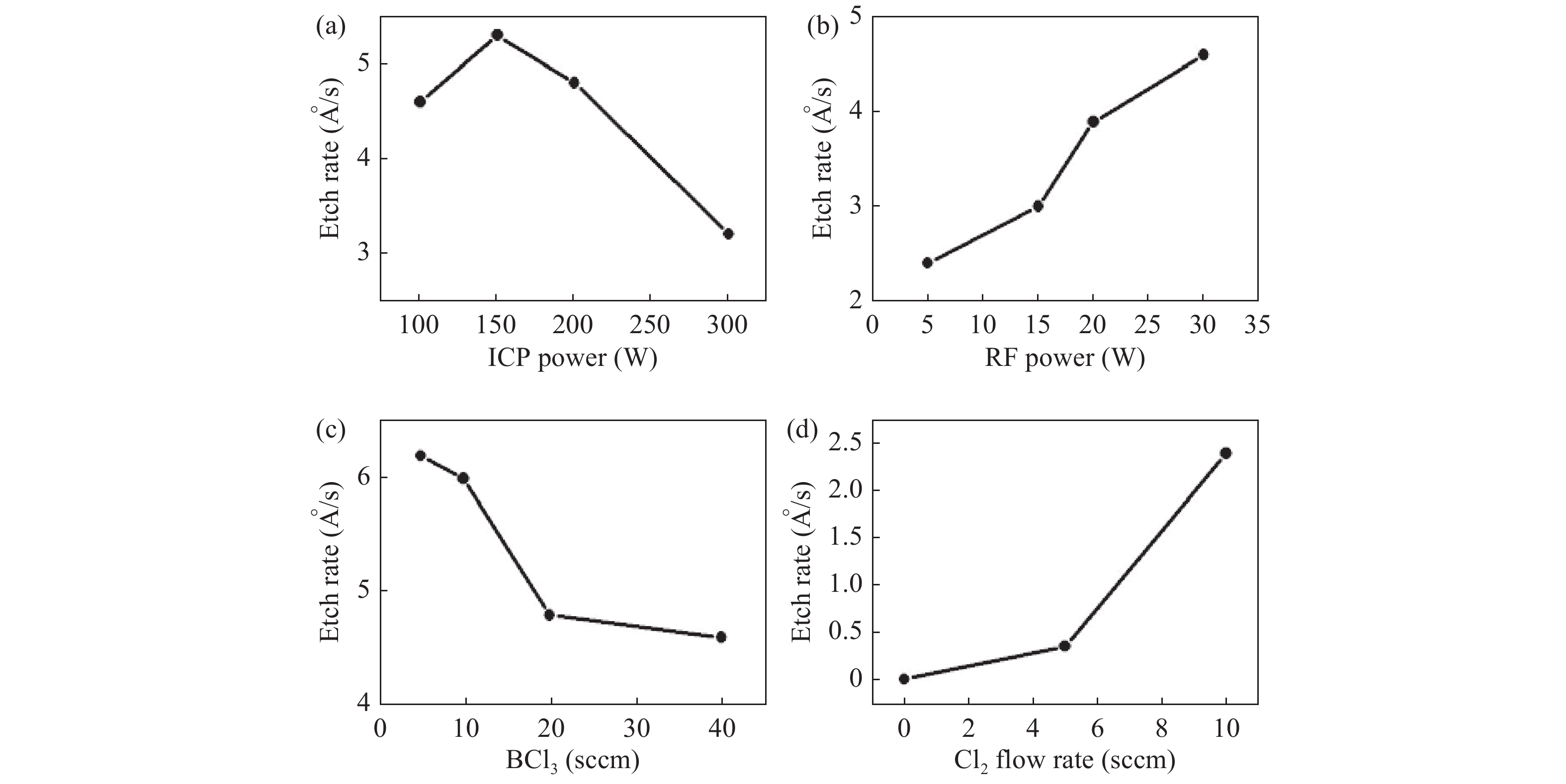
Fig. 1.  The etch rate variation with (a) ICP power, (b) RF power, (c) BCl3 flow rate and (d) Cl2 flow rate, respectively.

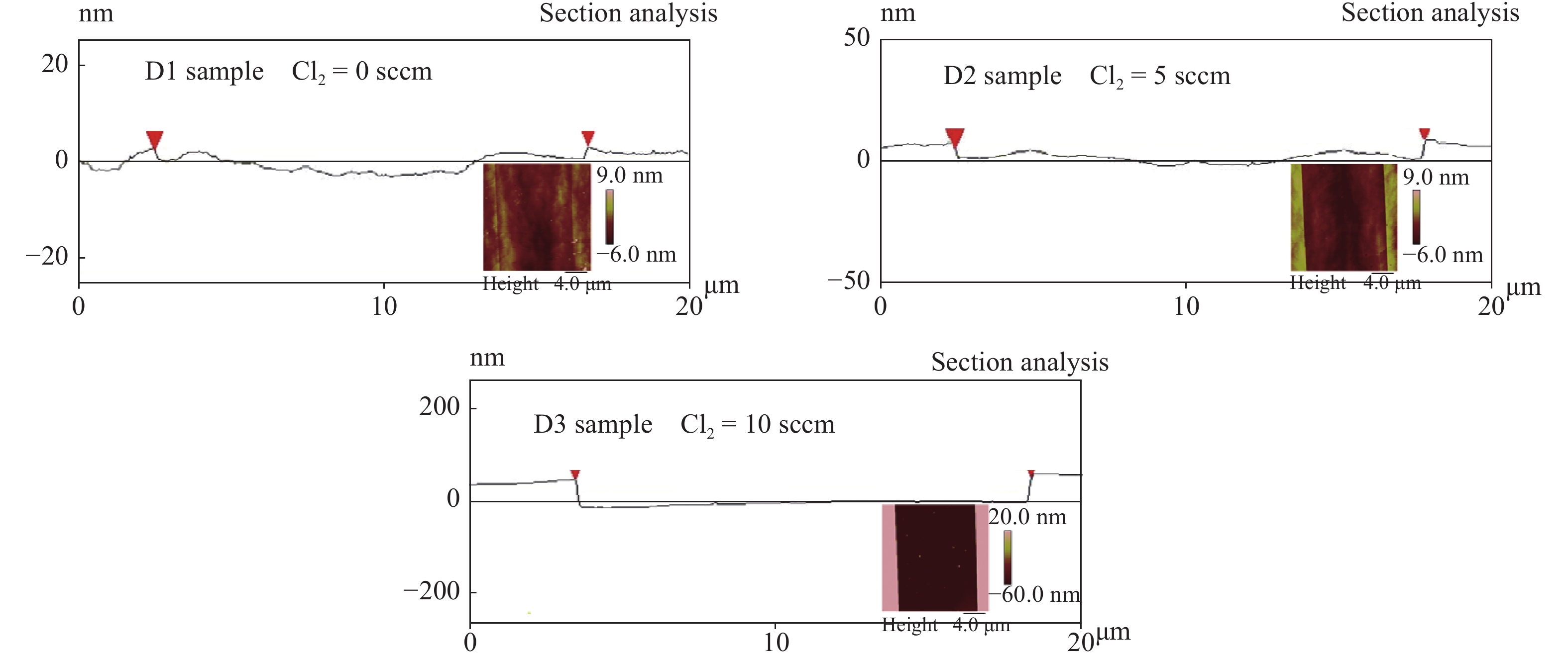
Fig. 2.  (Color online) AFM section height profiles of D1, D2 and D3 samples.

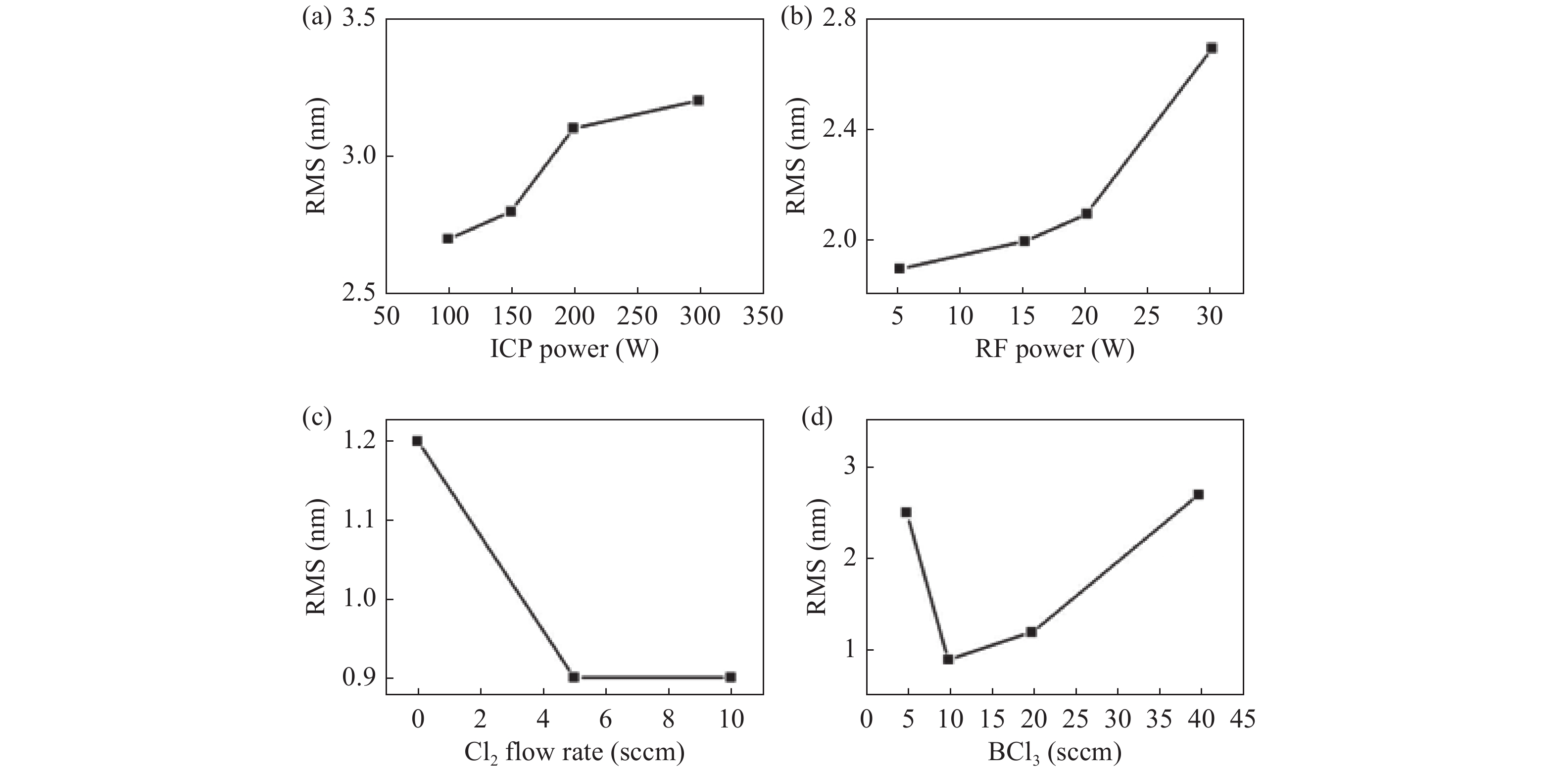
Fig. 3.  The RMS variation with (a) ICP power, (a) RF power, (c) Cl2 flow rate, and (d) BCl3 flow rate (d), respectively.

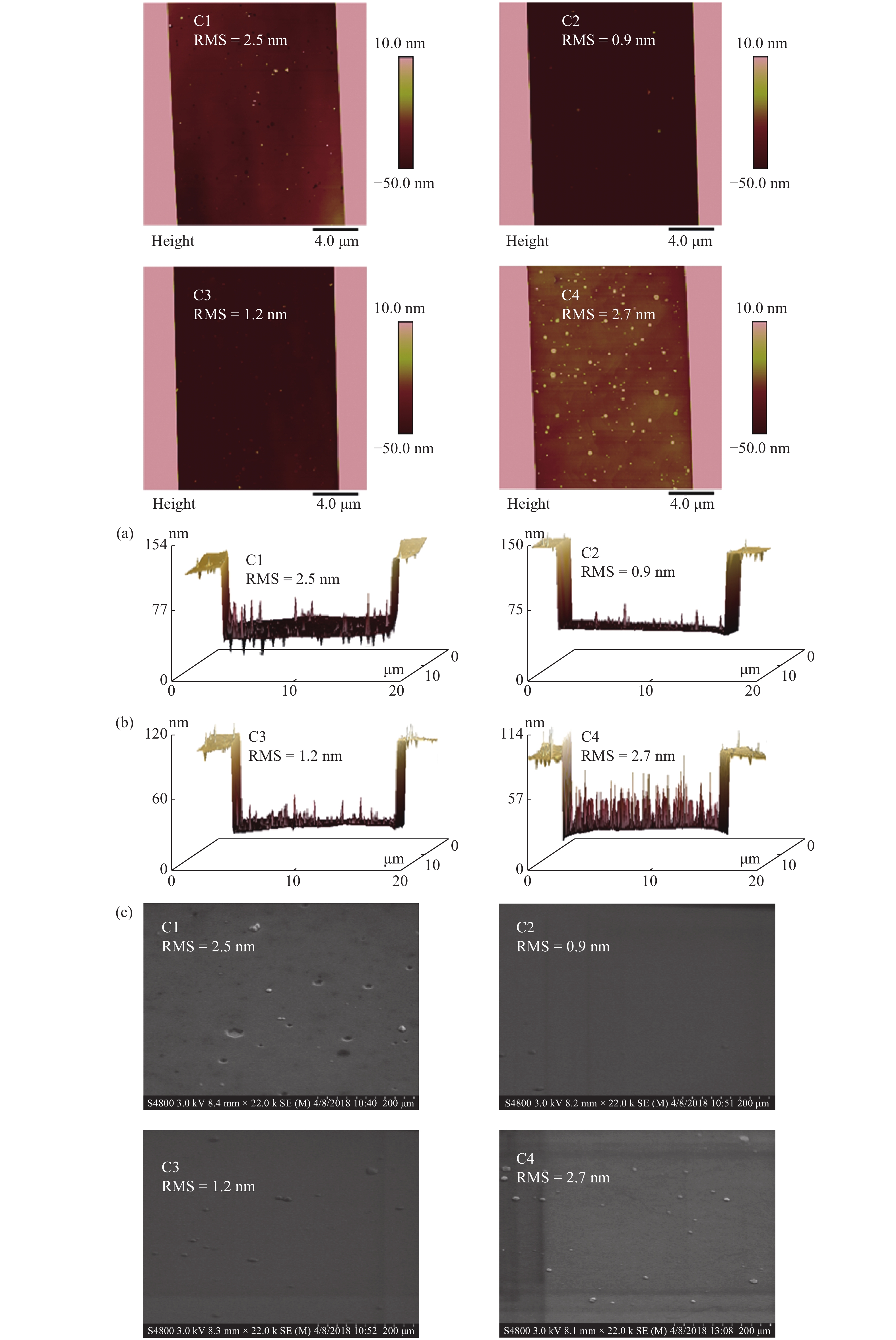
Fig. 4.  (Color online) 20 × 20 μm2 AFM (a) 2D height images and (b) 3D topography images of samples C1, C2, C3 and C4. Their surface topographies are pits and burrs, no pits, small burrs and large burrs, respectively. (c) SEM surface topography images of samples C1, C2, C3 and C4.

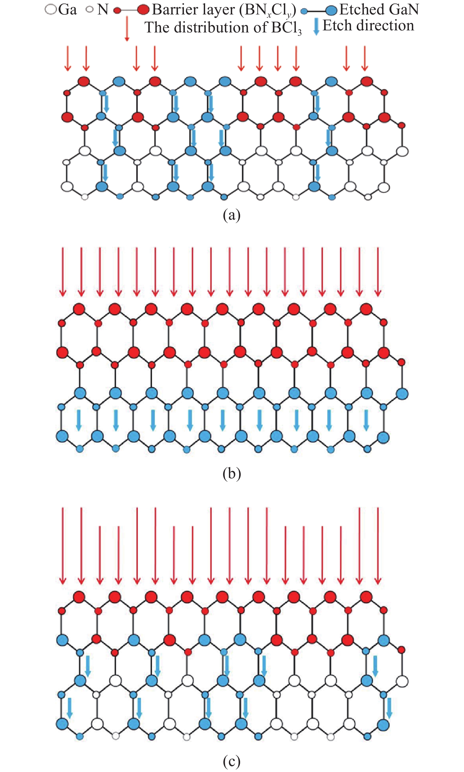
Fig. 5.  (Color online) (a) 2D simplified etch model of forming pits and burrs. The flow rate of BCl3 is slow (~5 sccm). (b) 2D simplified etch model of forming smooth etch surface. The flow rate of BCl3 is appropriate (10–20 sccm). (c) 2D simplified etch model of forming large burrs. The flow rate of BCl3 is fast (~40 sccm).

Table 1.   Some works on etch rate and etch surface RMS of GaN.

Researcher Etching rate (Å/s) ΔRMS (nm)
Zhou[15] 141 0.8
Rawal et al.[16] 21 Smooth and
clean (SEM)
Wang, Cai et al.[17] 7.1
Wakejima[18] 0.83
Arulkumaran et al.[19] 0.82
In this work 0.36 0.2
ΔRMS = RMS (after etching) – RMS (before etching)
DownLoad: CSV

Table 2.   The etching conditions of GaN corresponding to labeled A1–D3.

Parameter ICP power (W) RF power (W) BCl3 flow rate (sccm) Cl2 flow rate (sccm) Etch rate (Å/s) RMS (nm)
A1 100 30 40 5 4.6 2.7
A2 150 30 40 5 5.3 2.8
A3 200 30 40 5 4.8 3.1
A4 300 30 40 5 3.2 3.2
B1 100 5 40 5 2.4 1.9
B2 100 15 40 5 3.0 2.0
B3 100 20 40 5 3.9 2.1
B4(A1) 100 30 40 5 4.6 2.7
C1 100 30 5 5 6.2 2.5
C2 100 30 10 5 6.0 0.9
C3 100 30 20 5 4.8 1.2
C4(A1) 100 30 40 5 4.6 2.7
D1 100 5 10 0 0.01 1.2
D2 100 5 10 5 0.36 0.9
D3 100 5 10 10 2.4 0.9
DownLoad: CSV
[1]
Cordier Y, Semonda F, Lorenzini P, et al. MBE growth of AlGaN/GaN HEMTs on resistive Si(111) substrate with RF small signal and power performances. J Cryst Growth, 2003, 251(1): 811 doi: 10.1109/MBE.2002.1037778
[2]
Li G Q, Shih S J, Fu Z Y, et al. A new system for synthesis of high quality nonpolar GaN thin films. Chem Commun, 2010, 46(8): 1206 doi: 10.1039/B919722B
[3]
Li G Q, Wang W L, Yang W J, et al. Epitaxial growth of group III-nitride films by pulsed laser deposition and their use in the development of LED devices. Surf Sci Rep, 2015, 70: 380 doi: 10.1016/j.surfrep.2015.06.001
[4]
Yang W J, Wang W L, Lin Y H, et al. Deposition of nonpolar m-plane InGaN/GaN multiple quantum wells on LiGaO2(100) substrates. J Mater Chem C, 2014, 2: 801 doi: 10.1039/C3TC31935K
[5]
Li G Q, Wang W L, Yang W J, et al. GaN-based light-emitting diodes on various substrates: a critical review. Rep Prog Phys, 2016, 79: 45 doi: 0.1088/0034-4885/79/5/056501
[6]
Storm D F, Katzer D S, Roussos J A, et al. AlGaN/GaN HEMTs on free-standing GaN substrates: MBE growth and microwave characterization. J Cryst Growth, 2007, 301: 429 doi: doi.org/10.1016/j.jcrysgro.2006.11.085
[7]
Adesida I, Youtsey C, Ping A T. Dry and wet etching for group III–nitrides. MRS Proc, 1998: 537 doi: doi.org/10.1557/PROC-537-G1.4
[8]
Luo Y, Han Y J, Wu T, et al. Inductively coupled plasma etching of GaN-based materials. First Asia-Pacific Workshop on Wide Bandgap Semiconductors, 2003: 210
[9]
Qiu R F, Lu H, Chen D J, et al. Optimization of inductively coupled plasma deep etching of GaN and etching damage analysis. Appl Surf Sci, 2011, 257(15): 2700 doi: doi.org/10.1016/j.apsusc.2010.10.048
[10]
Shul R J, McClellan G B, Casalnuovo S A, et al. Inductively coupled plasma etching of GaN. Appl Phys Lett, 1996, 69(8): 1119 doi: 10.1063/1.117077
[11]
Cao X A, Zhang A P, Dang G T, et al. Schottky diode measurements of dry etch damage in n- and p-type GaN. J Vac Sci Technol, 2000, 18(4): 1144 doi: 10.1116/1.582314
[12]
Pearton S J, Lee J W, Mackenzie J D, et al. dry etch damage in InN, InGaN, and InAlN. Appl Phys Lett, 1995, 67(16): 2329 doi: 10.1063/1.114334
[13]
Cao X A, Cho H, Pearton S J, et al. Depth and thermal stability of dry etch damage in GaN Schottky diodes. Appl Phys Lett, 1999, 75(2): 232 doi: 10.1063/1.124332
[14]
Shul R J, Zhang L, Baca A G, et al. Inductively coupled plasma-induced etch damage of GaN p–n junctions. J Vac Sci Technol A, 2000, 18(4): 1139 doi: 10.1116/1.582313
[15]
Zhou S J, Cao B, Liu S. Dry etching characteristics of GaN using Cl2/BCl3 inductively coupled plasmas. Appl Surf Sci, 2010, 257: 905 doi: 10.1016/j.apsusc.2010.07.088
[16]
Rawal D S, Sehgal B K, Muralidharan R, et al. Effect of BCl3 concentration and process pressure on the GaN mesa sidewalls in BCl3/Cl2 based inductively coupled plasma etching. Vacuum, 2012, 86: 1844 doi: 10.1016/j.vacuum.2012.04.018
[17]
Wang W, Cai Y, Zhang B S, et al. The control of ICP etching GaN sidewall profiles and etch rate. Res Prog SSE, 2012, 32(3): 219
[18]
Wakejima A, Ando A, Watanabe A, et al. Normally off AlGaN/GaN HEMT on Si substrate with selectively dry etched recessed gate and polarization charge compensation δ-doped GaN cap layer. Appl Phys Express, 2015, 8(2): 37 doi: dx.doi.org/10.7567/APEX.8.026502
[19]
Arulkumaran S, Egaway T, Selvaraj L, et al. On the effects of gate-recess etching in current-collapse of different cap layers grown AlGaN/GaN high-electron-mobility transistors. Jpn J Appl Phys, 2006, 45(8): L220 doi: 10.1143/JJAP.45.L220
  • Search

    Advanced Search >>

    GET CITATION

    shu

    Export: BibTex EndNote

    Article Metrics

    Article views: 4158 Times PDF downloads: 81 Times Cited by: 0 Times

    History

    Received: 04 March 2018 Revised: 02 May 2018 Online: Uncorrected proof: 04 July 2018Published: 01 November 2018

    Catalog

      Email This Article

      User name:
      Email:*请输入正确邮箱
      Code:*验证码错误
      Xilin Li, Ping Ma, Xiaoli Ji, Tongbo Wei, Xiaoyu Tan, Junxi Wang, Jinmin Li. Implementation of slow and smooth etching of GaN by inductively coupled plasma[J]. Journal of Semiconductors, 2018, 39(11): 113002. doi: 10.1088/1674-4926/39/11/113002 ****X L Li, P Ma, X L Ji, T B Wei, X Y Tan, J X Wang, J M Li, Implementation of slow and smooth etching of GaN by inductively coupled plasma[J]. J. Semicond., 2018, 39(11): 113002. doi: 10.1088/1674-4926/39/11/113002.
      Citation:
      Xilin Li, Ping Ma, Xiaoli Ji, Tongbo Wei, Xiaoyu Tan, Junxi Wang, Jinmin Li. Implementation of slow and smooth etching of GaN by inductively coupled plasma[J]. Journal of Semiconductors, 2018, 39(11): 113002. doi: 10.1088/1674-4926/39/11/113002 ****
      X L Li, P Ma, X L Ji, T B Wei, X Y Tan, J X Wang, J M Li, Implementation of slow and smooth etching of GaN by inductively coupled plasma[J]. J. Semicond., 2018, 39(11): 113002. doi: 10.1088/1674-4926/39/11/113002.

      Implementation of slow and smooth etching of GaN by inductively coupled plasma

      doi: 10.1088/1674-4926/39/11/113002
      Funds:

      Project supported by the National Key R&D Program of China (No. 2017YFB0403001) and the National Natural Sciences Foundation of China (No. 61404134).

      More Information
      • Corresponding author: tbwei@semi.ac.cn
      • Received Date: 2018-03-04
      • Revised Date: 2018-05-02
      • Published Date: 2018-11-01

      Catalog

        /

        DownLoad:  Full-Size Img  PowerPoint
        Return
        Return