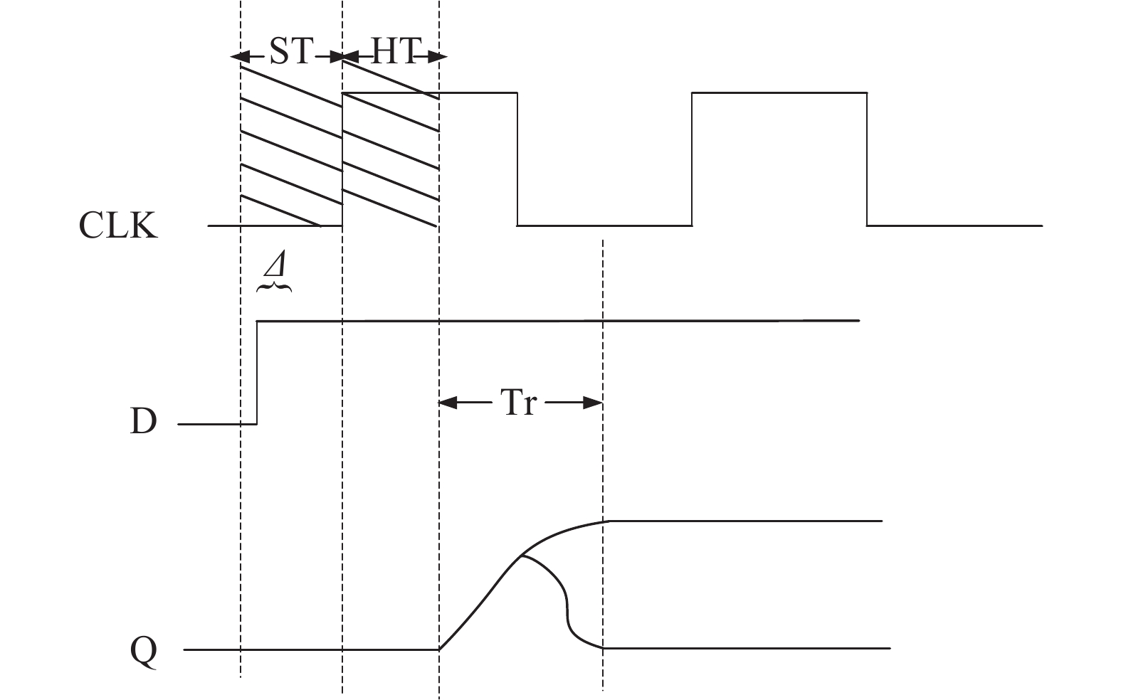
Fig. 1.
Metastability of a D flip-flop.
SEMICONDUCTOR INTEGRATED CIRCUITS
Hongzhen Fang1, Pengjun Wang1, , Xu Cheng2 and Keji Zhou2
Corresponding author: Pengjun Wang, Email: wangpengjun@nbu.edu.cn
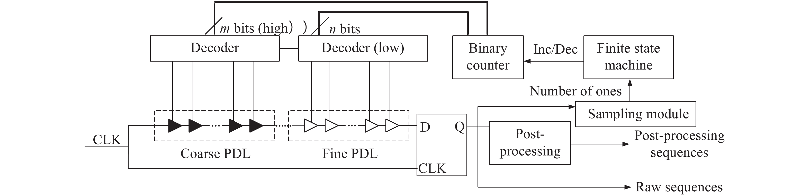
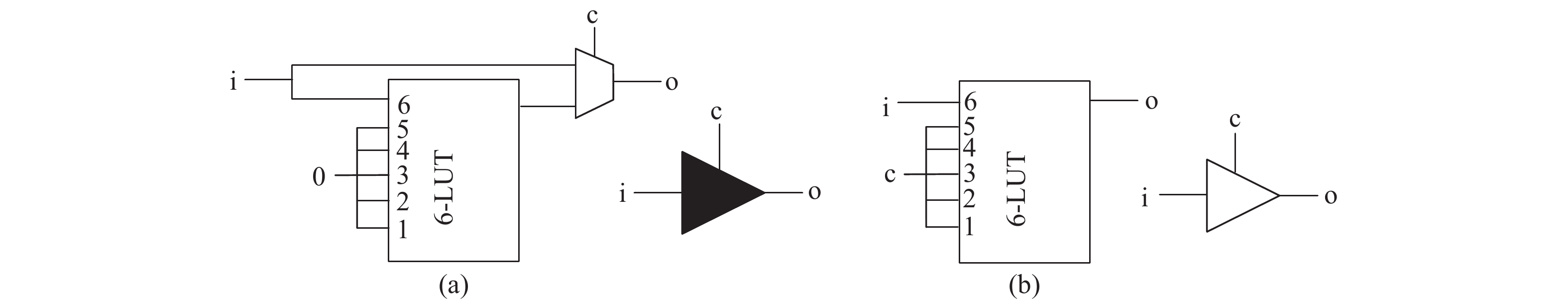
Abstract: A metastability-based TRNG (true random number generator) is presented in this paper, and implemented in FPGA. The metastable state of a D flip-flop is tunable through a two-stage PDL (programmable delay line). With the proposed coarse-tuning PDL structure, the TRNG core does not require extra placement and routing to ensure its entropy. Furthermore, the core needs fewer stages of coarse-tuning PDL at higher operating frequency, and thus saves more resources in FPGA. The designed TRNG achieves 25 Mbps @ 100 MHz throughput after proper post-processing, which is several times higher than other previous TRNGs based on FPGA. Moreover, the robustness of the system is enhanced with the adoption of a feedback system. The quality of the designed TRNG is verified by NIST (National Institute of Standards and Technology) and also accepted by class P1 of the AIS-20/31 test suite.
Keywords: TRNG, FPGA, metastability-based, coarse-tuning PDL
| [1] |
Drutarovsky M, Galajda P. A robust chaos-based true random number generator embedded in reconfigurable switched-capacitor hardware. 17th International Conference on Radioelektronika, 2007: 1
|
| [2] |
Simka M, Drutarovsky M, Fischer V, et al. Model of a true random number generator aimed at cryptographic applications. IEEE International Symposium on Circuits and Systems, 2006: 5619
|
| [3] |
Zhou T, Zhou Z B, Yu M Y, et al. A robust low power chaos-based truly random number generator. Chin J Semicond, 2008, 29(1): 69 (in Chinese)
|
| [4] |
Liu Y, Cheung R C C, Wong H. A bias-bounded digital true random number generator architecture. IEEE Trans Circuits Syst I, 2017, 64(1): 133 doi: 10.1109/TCSI.2016.2606353
|
| [5] |
Petrie C S, Connelly J A. A noise-based IC random number generator for applications in cryptography. IEEE Trans Circuits Syst I, 2000, 47(5): 615 doi: 10.1109/81.847868
|
| [6] |
Mathew S K, Johnston D, Satpathy S, et al. uRNG: A 300–950 mV, 323 Gbps/W all-digital full-entropy true random number generator in 14 nm FinFET CMOS. IEEE J Solid-State Circuits, 2016, 51(7): 1695 doi: 10.1109/JSSC.2016.2558490
|
| [7] |
Johnson A P, Rajat S C, Debdeep M. An improved DCM-based tunable true random number generator for Xilinx FPGA. IEEE Trans Circuits Syst II, 2017, 64(4): 452 doi: 10.1109/TCSII.2016.2566262
|
| [8] |
Wieczorek P Z, Golofit K. Dual-metastability time-competitive true random number generator. IEEE Transn Circuits Syst I, 2014, 61(1): 134 doi: 10.1109/TCSI.2013.2265952
|
| [9] |
Wieczorek P Z. An FPGA implementation of the resolve time-based true random number generator with quality control. IEEE Trans Circuits Syst I, 2014, 61(12): 3450 doi: 10.1109/TCSI.2014.2338615
|
| [10] |
Hisashi H, Ichikawa S. FPGA implementation of metastability-based true random number generator. IEICE Trans Inform Syst, 2012, 95(2): 426
|
| [11] |
Majzoobi M, Koushanfar F, Devadas S. FPGA-based true random number generation using circuit metastability with adaptive feedback control. International Workshop on Cryptographic Hardware and Embedded Systems. Berlin: Springer, 2011: 17
|
| [12] |
Figueiredo P M. Comparator metastability in the presence of noise. IEEE Trans Circuits Syst I, 2013, 60(5): 1286 doi: 10.1109/TCSI.2012.2221195
|
| [13] |
Ou H W, Zhao J, Li Q R. Post-processing method in truly random number generator. Comput Sci, 2012, 39(B06): 9
|
| [14] |
Tsuneda A, Sugahara T, Inoue T. Statistical properties of modulo-2 added binary sequences. IEICE Trans Fundam Electron, Commun Comput Sci, 2004, 87(9): 2267
|
| [15] |
Danger J L, Guilley S, Hoogvorst P. Fast true random generator in FPGAs. IEEE Northeast Workshop on Circuits and Systems, 2007: 506
|
| [16] |
Varchola M, Drutarovsky M. New high entropy element for FPGA based true random number generators. International Workshop on Cryptographic Hardware and Embedded Systems. Berlin: Springer, 2010: 351
|
| [17] |
Xu X, Wang Y. High speed true random number generator based on FPGA. International Conference on Information Systems Engineering (ICISE) Conference, 2016: 18
|
| [18] |
Rozic V, Yang B, Dehaene W, et al. Highly efficient entropy extraction for true random number generators on FPGAs. 52nd ACM/EDAC/IEEE Design Automation Conference (DAC), 2015: 1
|
| [19] |
Bae S G, Kim Y, Park Y, et al. 3-Gb/s high-speed true random number generator using common-mode operating comparator and sampling uncertainty of D flip-flop. IEEE J Solid-State Circuits, 2017, 52(2): 605 doi: 10.1109/JSSC.2016.2625341
|
| [20] |
Peng, Y M, Zhao H B, Sun X, et al. A side-channel attack resistant AES with 500 Mbps, 1.92 pJ/bit PVT variation tolerant true random number generator. IEEE Computer Society Annual Symposium on VLSI, 2017: 249
|
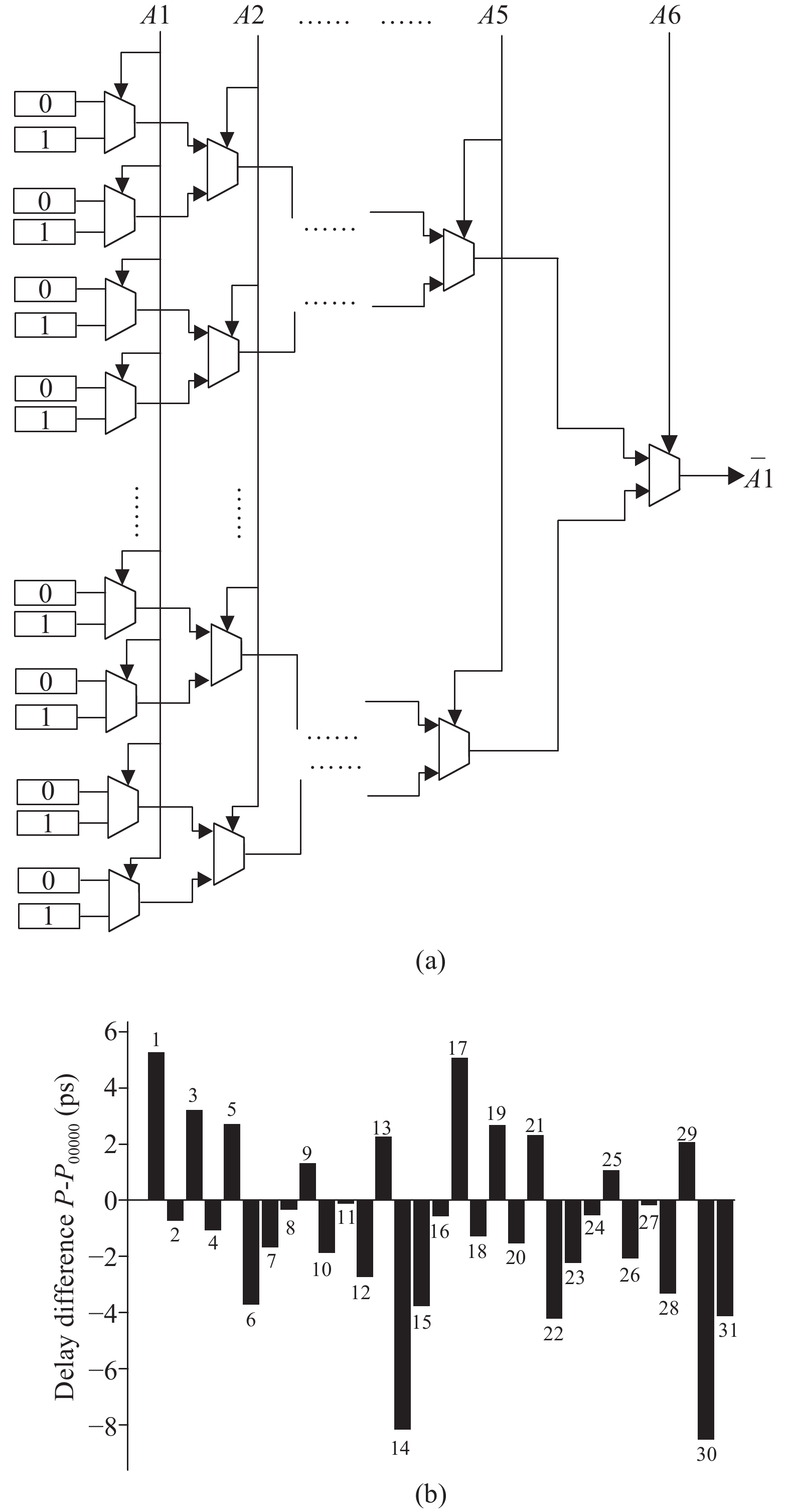
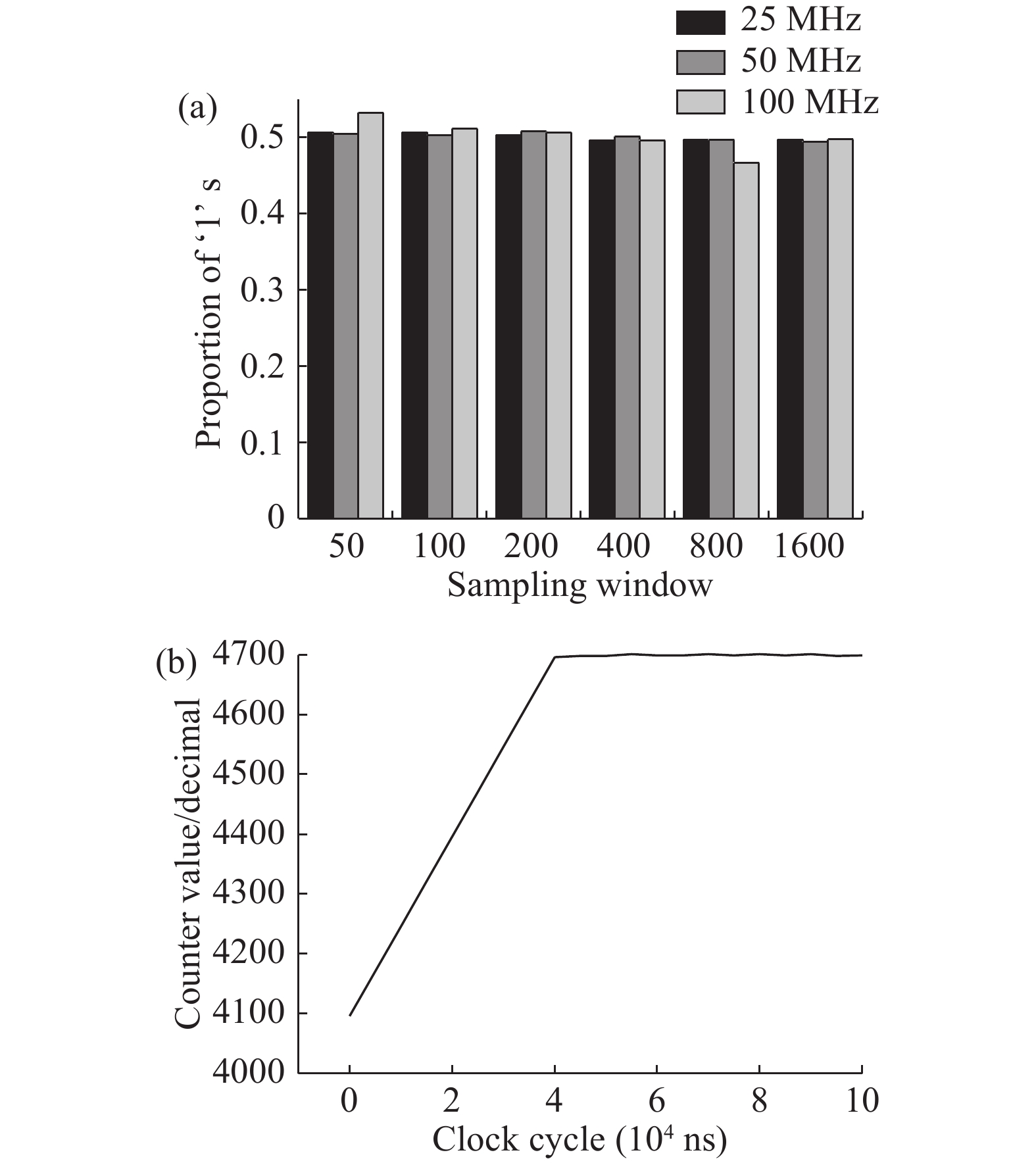
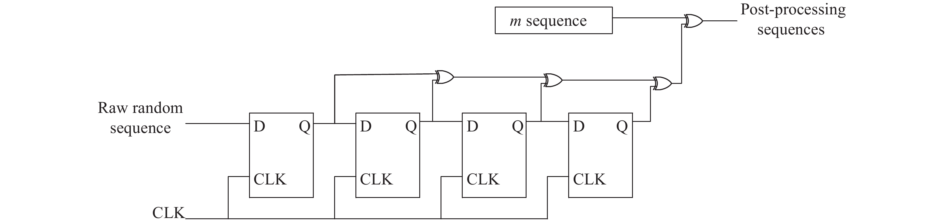
Table 1. Tuning levels of the counter value with different proportions of ‘1’s.
| Proportion of ‘1’s | Tuning level of counter value |
| ≥80% | +3 |
| 52%–80% | +1 |
| 48%–52% | +0 |
| 20%–48% | −1 |
| ≤20% | −3 |
 DownLoad: CSV
Table 2. Test results of NIST for post-processing sequences of the three employed frequencies.
| NIST ↓ TRNG → | 100 MHz (170 LUTs) | 50 MHz (290 LUTs) | 25 MHz (530 LUTs) | ||||||
| TEST SUITE | p-value | Proportion | p-value | Proportion | p-value | Proportion | |||
| Frequency | 0.1045 | 0.9733 | 0.3986 | 0.9904 | 0.8916 | 0.9904 | |||
| Block frequency | 0.0451 | 0.9809 | 0.8301 | 0.9952 | 0.0451 | 0.9809 | |||
| Cumulative sums | 0.2881 | 0.9833 | 0.2715 | 0.9880 | 0.4685 | 0.9952 | |||
| Runs | 0.1094 | 0.9667 | 0.6519 | 1 | 0.2474 | 0.9952 | |||
| Longest run of ones | 0.1257 | 0.9857 | 0.2856 | 0.9857 | 0.4777 | 0.9952 | |||
| Rank | 0.9372 | 0.9867 | 0.7541 | 1 | 0.2053 | 0.9733 | |||
| Discrete Fourier transform | 0.3661 | 1 | 0.2992 | 1 | 0.0896 | 0.9809 | |||
| Nonperiodic template matchings | 0.4840 | 0.9900 | 0.4992 | 0.9890 | 0.5017 | 0.9890 | |||
| Overlapping template matchings | 0.2597 | 0.9904 | 0.7887 | 0.9583 | 0.8165 | 0.9602 | |||
| Universal statistical | 0.3621 | 0.9733 | 0.4915 | 1 | 0.3621 | 0.9733 | |||
| Approximate entropy | 0.0649 | 0.9952 | 0.2597 | 0.9809 | 0.8216 | 0.9857 | |||
| Random excursions | 0.3922 | 0.9950 | 0.1798 | 0.9957 | 0.2806 | 0.9950 | |||
| Random excursions variant | 0.2848 | 1 | 0.1267 | 0.9981 | 0.2378 | 0.9978 | |||
| Serial | 0.3539 | 0.9928 | 0.6321 | 0.9880 | 0.4353 | 0.9833 | |||
| Linear complexity | 0.8773 | 0.9714 | 0.0575 | 0.9761 | 0.7773 | 0.9809 | |||
DownLoad: CSV
Table 3. Test results of AIS-20/31 for post-processing sequences (T0–T5) and raw sequences (T6–T8) of the three employed frequencies.
| Parameter | 100 MHz (170 LUTs) | 50 MHz (290 LUTs) | 25 MHz (530 LUTs) |
| T0-Disjointness | Pass | Pass | Pass |
| T1-Monobit | Pass | Pass | Pass |
| T2-Poker | Pass | Pass | Pass |
| T3-Runs | Pass | Pass | Pass |
| T4-LongRuns | Pass | Pass | Pass |
| T5-Autocorrelation | Pass | Pass | Pass |
| T6-UniformA | Fail | Fail | Fail |
| T6-UniformB | Fail | Fail | Fail |
| T7-HomogeneityA | Pass | Pass | Pass |
| T7-HomogeneityB | Pass | Pass | Pass |
| T8-Entropy | Fail | Fail | Fail |
DownLoad: CSV
Table 4. Comparison of the designed TRNG with other methodologies in FPGA.
| References | Methodology | Device | Resources used by TRNG core | Bit rate (Mbps) | Operating frequency (MHz) |
| This work | Deep meta state | Altera Stratix IV | 170 LUTs + DFF | 25 | 100 |
| Ref. [9] | Nearly meta state | Xilinx XC6SLX16 | 36 LUTs + 24 DFFs | 12.6 | – |
| Ref. [10] | Deep meta state | Xilinx XC4VFX 20 | 256 latches | 12.5 | – |
| Ref. [11] | Deep meta state | Xilinx Virtex 5 | 128 LUTs + DFF | 2.5 | – |
| Ref. [15] | Deep meta state | Altera EPIS 25 | 100 latches | 20 | 20 |
| Ref. [16] | TERO | Xilinx Spartan 3E | 2 TREOs | 0.25 | 0.25 |
| Ref. [17] | Clock jitter | Xilinx Virtex-II | DCM + DFF | 6.05 | 270 |
| Ref. [18] | Ring oscillator | Xilinx Spartan 6 | 3 slices | 1.53 | 100 |
| Ref. [19] | Deep meta state | 65 nm | 1609 μm2 | 3000 | 3000 |
| Ref. [20] | Deep meta state | 130 nm | 9488 μm2 | 500 | 500 |
DownLoad: CSV
| [1] |
Drutarovsky M, Galajda P. A robust chaos-based true random number generator embedded in reconfigurable switched-capacitor hardware. 17th International Conference on Radioelektronika, 2007: 1
|
| [2] |
Simka M, Drutarovsky M, Fischer V, et al. Model of a true random number generator aimed at cryptographic applications. IEEE International Symposium on Circuits and Systems, 2006: 5619
|
| [3] |
Zhou T, Zhou Z B, Yu M Y, et al. A robust low power chaos-based truly random number generator. Chin J Semicond, 2008, 29(1): 69 (in Chinese)
|
| [4] |
Liu Y, Cheung R C C, Wong H. A bias-bounded digital true random number generator architecture. IEEE Trans Circuits Syst I, 2017, 64(1): 133 doi: 10.1109/TCSI.2016.2606353
|
| [5] |
Petrie C S, Connelly J A. A noise-based IC random number generator for applications in cryptography. IEEE Trans Circuits Syst I, 2000, 47(5): 615 doi: 10.1109/81.847868
|
| [6] |
Mathew S K, Johnston D, Satpathy S, et al. uRNG: A 300–950 mV, 323 Gbps/W all-digital full-entropy true random number generator in 14 nm FinFET CMOS. IEEE J Solid-State Circuits, 2016, 51(7): 1695 doi: 10.1109/JSSC.2016.2558490
|
| [7] |
Johnson A P, Rajat S C, Debdeep M. An improved DCM-based tunable true random number generator for Xilinx FPGA. IEEE Trans Circuits Syst II, 2017, 64(4): 452 doi: 10.1109/TCSII.2016.2566262
|
| [8] |
Wieczorek P Z, Golofit K. Dual-metastability time-competitive true random number generator. IEEE Transn Circuits Syst I, 2014, 61(1): 134 doi: 10.1109/TCSI.2013.2265952
|
| [9] |
Wieczorek P Z. An FPGA implementation of the resolve time-based true random number generator with quality control. IEEE Trans Circuits Syst I, 2014, 61(12): 3450 doi: 10.1109/TCSI.2014.2338615
|
| [10] |
Hisashi H, Ichikawa S. FPGA implementation of metastability-based true random number generator. IEICE Trans Inform Syst, 2012, 95(2): 426
|
| [11] |
Majzoobi M, Koushanfar F, Devadas S. FPGA-based true random number generation using circuit metastability with adaptive feedback control. International Workshop on Cryptographic Hardware and Embedded Systems. Berlin: Springer, 2011: 17
|
| [12] |
Figueiredo P M. Comparator metastability in the presence of noise. IEEE Trans Circuits Syst I, 2013, 60(5): 1286 doi: 10.1109/TCSI.2012.2221195
|
| [13] |
Ou H W, Zhao J, Li Q R. Post-processing method in truly random number generator. Comput Sci, 2012, 39(B06): 9
|
| [14] |
Tsuneda A, Sugahara T, Inoue T. Statistical properties of modulo-2 added binary sequences. IEICE Trans Fundam Electron, Commun Comput Sci, 2004, 87(9): 2267
|
| [15] |
Danger J L, Guilley S, Hoogvorst P. Fast true random generator in FPGAs. IEEE Northeast Workshop on Circuits and Systems, 2007: 506
|
| [16] |
Varchola M, Drutarovsky M. New high entropy element for FPGA based true random number generators. International Workshop on Cryptographic Hardware and Embedded Systems. Berlin: Springer, 2010: 351
|
| [17] |
Xu X, Wang Y. High speed true random number generator based on FPGA. International Conference on Information Systems Engineering (ICISE) Conference, 2016: 18
|
| [18] |
Rozic V, Yang B, Dehaene W, et al. Highly efficient entropy extraction for true random number generators on FPGAs. 52nd ACM/EDAC/IEEE Design Automation Conference (DAC), 2015: 1
|
| [19] |
Bae S G, Kim Y, Park Y, et al. 3-Gb/s high-speed true random number generator using common-mode operating comparator and sampling uncertainty of D flip-flop. IEEE J Solid-State Circuits, 2017, 52(2): 605 doi: 10.1109/JSSC.2016.2625341
|
| [20] |
Peng, Y M, Zhao H B, Sun X, et al. A side-channel attack resistant AES with 500 Mbps, 1.92 pJ/bit PVT variation tolerant true random number generator. IEEE Computer Society Annual Symposium on VLSI, 2017: 249
|


Article views: 4828 Times PDF downloads: 109 Times Cited by: 0 Times
Received: 19 July 2017 Revised: 27 August 2017 Online: Uncorrected proof: 24 January 2018Published: 01 March 2018
| Citation: |
Hongzhen Fang, Pengjun Wang, Xu Cheng, Keji Zhou. High speed true random number generator with a new structure of coarse-tuning PDL in FPGA[J]. Journal of Semiconductors, 2018, 39(3): 035001. doi: 10.1088/1674-4926/39/3/035001
****
H Z Fang, P J Wang, X Cheng, K J Zhou. High speed true random number generator with a new structure of coarse-tuning PDL in FPGA[J]. J. Semicond., 2018, 39(3): 035001. doi: 10.1088/1674-4926/39/3/035001.

|
| [1] |
Drutarovsky M, Galajda P. A robust chaos-based true random number generator embedded in reconfigurable switched-capacitor hardware. 17th International Conference on Radioelektronika, 2007: 1
|
| [2] |
Simka M, Drutarovsky M, Fischer V, et al. Model of a true random number generator aimed at cryptographic applications. IEEE International Symposium on Circuits and Systems, 2006: 5619
|
| [3] |
Zhou T, Zhou Z B, Yu M Y, et al. A robust low power chaos-based truly random number generator. Chin J Semicond, 2008, 29(1): 69 (in Chinese)
|
| [4] |
Liu Y, Cheung R C C, Wong H. A bias-bounded digital true random number generator architecture. IEEE Trans Circuits Syst I, 2017, 64(1): 133 doi: 10.1109/TCSI.2016.2606353
|
| [5] |
Petrie C S, Connelly J A. A noise-based IC random number generator for applications in cryptography. IEEE Trans Circuits Syst I, 2000, 47(5): 615 doi: 10.1109/81.847868
|
| [6] |
Mathew S K, Johnston D, Satpathy S, et al. uRNG: A 300–950 mV, 323 Gbps/W all-digital full-entropy true random number generator in 14 nm FinFET CMOS. IEEE J Solid-State Circuits, 2016, 51(7): 1695 doi: 10.1109/JSSC.2016.2558490
|
| [7] |
Johnson A P, Rajat S C, Debdeep M. An improved DCM-based tunable true random number generator for Xilinx FPGA. IEEE Trans Circuits Syst II, 2017, 64(4): 452 doi: 10.1109/TCSII.2016.2566262
|
| [8] |
Wieczorek P Z, Golofit K. Dual-metastability time-competitive true random number generator. IEEE Transn Circuits Syst I, 2014, 61(1): 134 doi: 10.1109/TCSI.2013.2265952
|
| [9] |
Wieczorek P Z. An FPGA implementation of the resolve time-based true random number generator with quality control. IEEE Trans Circuits Syst I, 2014, 61(12): 3450 doi: 10.1109/TCSI.2014.2338615
|
| [10] |
Hisashi H, Ichikawa S. FPGA implementation of metastability-based true random number generator. IEICE Trans Inform Syst, 2012, 95(2): 426
|
| [11] |
Majzoobi M, Koushanfar F, Devadas S. FPGA-based true random number generation using circuit metastability with adaptive feedback control. International Workshop on Cryptographic Hardware and Embedded Systems. Berlin: Springer, 2011: 17
|
| [12] |
Figueiredo P M. Comparator metastability in the presence of noise. IEEE Trans Circuits Syst I, 2013, 60(5): 1286 doi: 10.1109/TCSI.2012.2221195
|
| [13] |
Ou H W, Zhao J, Li Q R. Post-processing method in truly random number generator. Comput Sci, 2012, 39(B06): 9
|
| [14] |
Tsuneda A, Sugahara T, Inoue T. Statistical properties of modulo-2 added binary sequences. IEICE Trans Fundam Electron, Commun Comput Sci, 2004, 87(9): 2267
|
| [15] |
Danger J L, Guilley S, Hoogvorst P. Fast true random generator in FPGAs. IEEE Northeast Workshop on Circuits and Systems, 2007: 506
|
| [16] |
Varchola M, Drutarovsky M. New high entropy element for FPGA based true random number generators. International Workshop on Cryptographic Hardware and Embedded Systems. Berlin: Springer, 2010: 351
|
| [17] |
Xu X, Wang Y. High speed true random number generator based on FPGA. International Conference on Information Systems Engineering (ICISE) Conference, 2016: 18
|
| [18] |
Rozic V, Yang B, Dehaene W, et al. Highly efficient entropy extraction for true random number generators on FPGAs. 52nd ACM/EDAC/IEEE Design Automation Conference (DAC), 2015: 1
|
| [19] |
Bae S G, Kim Y, Park Y, et al. 3-Gb/s high-speed true random number generator using common-mode operating comparator and sampling uncertainty of D flip-flop. IEEE J Solid-State Circuits, 2017, 52(2): 605 doi: 10.1109/JSSC.2016.2625341
|
| [20] |
Peng, Y M, Zhao H B, Sun X, et al. A side-channel attack resistant AES with 500 Mbps, 1.92 pJ/bit PVT variation tolerant true random number generator. IEEE Computer Society Annual Symposium on VLSI, 2017: 249
|

 WeChat ID
Journal of Semiconductors © 2017 All Rights Reserved 京ICP备05085259号-2