SEMICONDUCTOR DEVICES

Small-signal model parameter extraction of E-mode N-polar GaN MOS-HEMT using optimization algorithms and its comparison

D. K. Panda, G. Amarnath and T. R. Lenka

+ Author Affiliations

 Corresponding author: T. R. Lenka, E-mail: t.r.lenka@ieee.org

PDF

Turn off MathJax

Abstract: An improved small-signal parameter extraction technique for short channel enhancement-mode N-polar GaN MOS-HEMT is proposed, which is a combination of a conventional analytical method and optimization techniques. The extrinsic parameters such as parasitic capacitance, inductance and resistance are extracted under the pinch-off condition. The intrinsic parameters of the small-signal equivalent circuit (SSEC) have been extracted including gate forward and backward conductance. Different optimization algorithms such as PSO, Quasi Newton and Firefly optimization algorithm is applied to the extracted parameters to minimize the error between modeled and measured S-parameters. The different optimized SSEC models have been validated by comparing the S-parameters and unity current-gain with TCAD simulations and available experimental data from the literature. It is observed that the Firefly algorithm based optimization approach accurately extracts the small-signal model parameters as compared to other optimization algorithm techniques with a minimum error percentage of 1.3%.

Key words: FireflyGaNMOS-HEMTPSOSSECTCAD


[1]
Panda D K, Lenka T R. Modeling and simulation of enhancement mode p-GaN Gate AlGaN/GaN HEMT for RF circuit switch applications. J Semicond, 2017, 38(6): 064002 doi: 10.1088/1674-4926/38/6/064002
[2]
Panda D K, Lenka T R. Oxide thickness dependent compact model of channel noise for E-mode AlGaN/GaN MOS-HEMT. AEU - Int J Electron Commun, 2017, 82: 467 doi: 10.1016/j.aeue.2017.09.025
[3]
Jena K, Swain R, Lenka T R. Impact of barrier thickness on gate capacitance-modeling and comparative analysis of GaN based MOSHEMTs. J Semicond, 2015, 36(3): 034003 doi: 10.1088/1674-4926/36/3/034003
[4]
Panda D K, Lenka T R. Effects of trap density on drain current LFN and its model development for E-mode GaN MOS-HEMT. Superlattices Microstruct, 2017, 112: 374 doi: 10.1016/j.spmi.2017.09.045
[5]
Chen M. A 1–25 GHz GaN HEMT MMIC low-noise amplifier. IEEE Microwave Wireless Compon Lett, 20(10): 563
[6]
Sun H F, Alt A R, Benedickter H, et al. High-speed and low-noise AlInN/GaN HEMTs on SiC. Phys Status Solidi A, 2011, 208(2): 429 doi: 10.1002/pssa.201000518
[7]
Chen M Q, Sutton W, Smorchkova, et al. A 1–25 GHz GaN HEMT MMIC low-noise amplifier. IEEE Microwave Wireless Compon Lett, 2010, 20(10): 563 doi: 10.1109/LMWC.2010.2059002
[8]
Sun H F, Alt A R, Benedickter H, et al. Low-noise microwave performance of 0.1 μm gate AlInN/GaN HEMTs on SiC. IEEE Microwave Wireless Compon Lett, 2010, 20(8): 453 doi: 10.1109/LMWC.2010.2049008
[9]
Li B, Wei L, Wen C. Static characteristics and short channel effect in enhancement-mode AlN/GaN/AlN N-polar MISFET with self-aligned source/drain regions. J Semicond, 2014, 35(12): 124006 doi: 10.1088/1674-4926/35/12/124006
[10]
Singisetti U, Wong M H, Speck J S, et al. Enhancement-mode N-polar GaN MOS-HFET with 5-nm GaN channel, 510-mS/mm gm, and 0.66- ohm·mm Ron’. IEEE Electron Device Lett, 2012, 33(1): 6 doi: 10.1109/LED.2011.2178050
[11]
Essaadali R, Jarndal A, Kouki A B, et al. A new GaN HEMT equivalent circuit modeling technique based on X-parameters. IEEE Trans Microwave Theory Tech, 2016, 64(9): 2758 doi: 10.1109/TMTT.2016.2594234
[12]
Alt A R, Marti D, Bolognesi C R. Transistor modeling: robust small-signal equivalent circuit extraction in various HEMT technologies. IEEE Microwave Mag, 2013, 14(4): 83 doi: 10.1109/MMM.2013.2248593
[13]
Du J, Xu P, Wang K, et al. Small-signal modeling of AlGaN/GaN HEMTs with consideration of CPW capacitances. J Semicond, 2015, 36(3): 34009 doi: 10.1088/1674-4926/36/3/034009
[14]
Crupi G, Schreurs D M M P, Caddemi A, et al. High-frequency extraction of the extrinsic capacitances for GaN HEMT technology. IEEE Microwave Wireless Compon Lett, 2011, 21(8): 445 doi: 10.1109/LMWC.2011.2160525
[15]
Resca D, Raffo A, Santarelli A, et al. Scalable equivalent circuit FET model for MMIC design identified through FW-EM analyses. IEEE Trans Microwave Theory Tech, 2009, 57(2): 245 doi: 10.1109/TMTT.2008.2011208
[16]
Snowden C M. Large-signal microwave characterization of AlGaAs/GaAs HBT's based on a physics-based electrothermal model. IEEE Trans Microwave Theory Tech, 1997, 45(1): 58 doi: 10.1109/22.552033
[17]
Majumdar A, Chatterjee S, Chatterjee S, et al. Optimization of intrinsic elements from small-signalmodel of GaN HEMT by using PSO. IEEE Applied Electromagnetics Conference (AEMC), Guwahati, 2015: . 1
[18]
Kumar R, Rajan A, Talukdar F A, et al. Optimization of 5.5-GHz CMOS LNA parameters using firefly algorithm. Neural Computing and Applications, 2016: 1
[19]
Brady R G, Oxley C H, Brazil T J. An improved small-signal parameter-extraction algorithm for GaN HEMT devices. IEEE Trans Microwave Theory Tech, 2008, 56(7): 1535 doi: 10.1109/TMTT.2008.925212
[20]
Dambrine G, Cappy A, Heliodore F, et al. A new method for determining the FET small-signal equivalent circuit. IEEE Trans Microwave Theory Tech, 1988, 36(7): 1151 doi: 10.1109/22.3650
[21]
Jarndal A, Kompa G. A new small-signal modeling approach applied to GaN devices. IEEE Trans Microwave Theory Tech, 2005, 53(11): 3440 doi: 10.1109/TMTT.2005.857332
[22]
Yanagawa S, Ishihara H, Ohtomo M. Analytical method for determining equivalent circuit parameters of GaAs FETs. IEEE Trans Microwave Theory Tech, 1996, 44(10): 1637 doi: 10.1109/22.538954
[23]
Nidhi, Dasgupta S, Keller S, et al. N-Polar GaN/AlN MIS-HEMT with fMAX of 204 GHz for Ka-band applications. IEEE Electron Device Lett, 2011, 32(12): 1683 doi: 10.1109/LED.2011.2168558
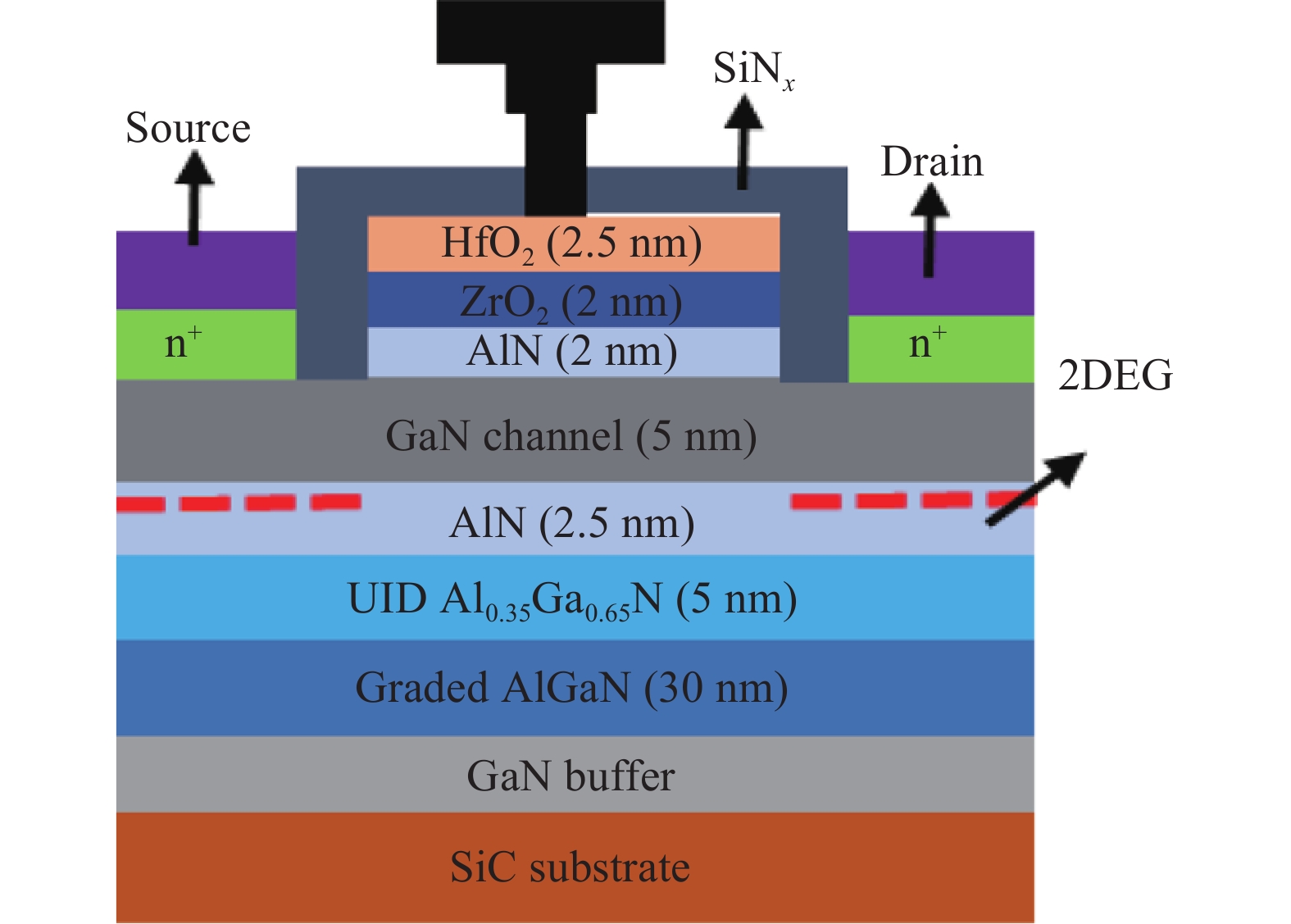
Fig. 1.  (Color online) Schematic diagram of N-polar GaN MOS-HEMT with 115 nm gate length.

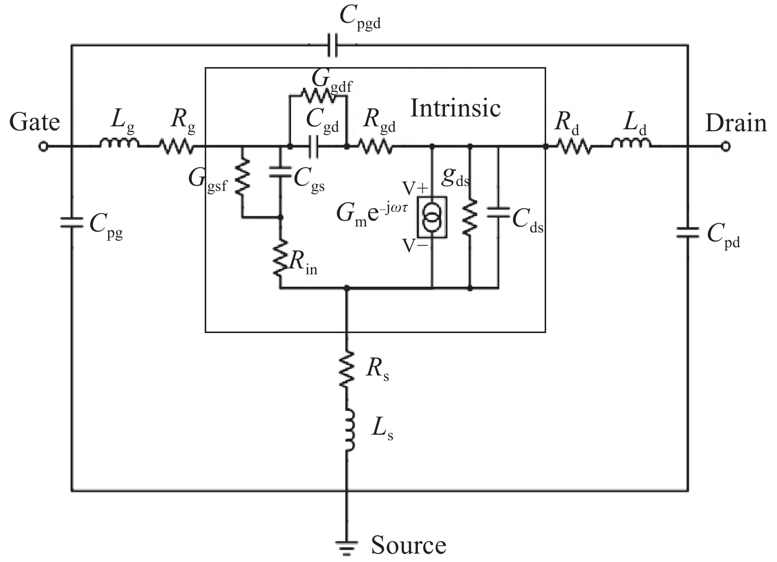
Fig. 2.  Small-signal equivalent circuit of N-polar GaN MOS-HEMT.

Fig. 3.  Equivalent circuit of MOS-HEMT at low frequency.

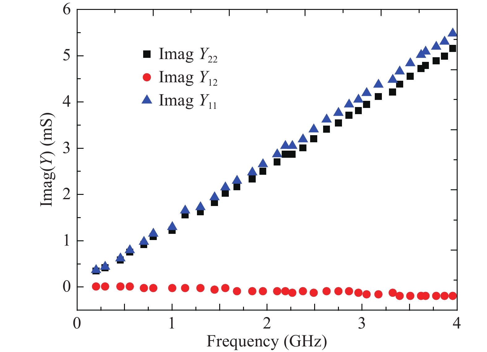
Fig. 4.  (Color online) Plot of Imag (Yij) versus frequency.

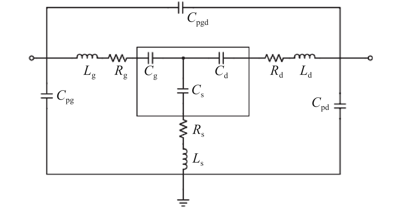
Fig. 5.  SSEC at high frequency.

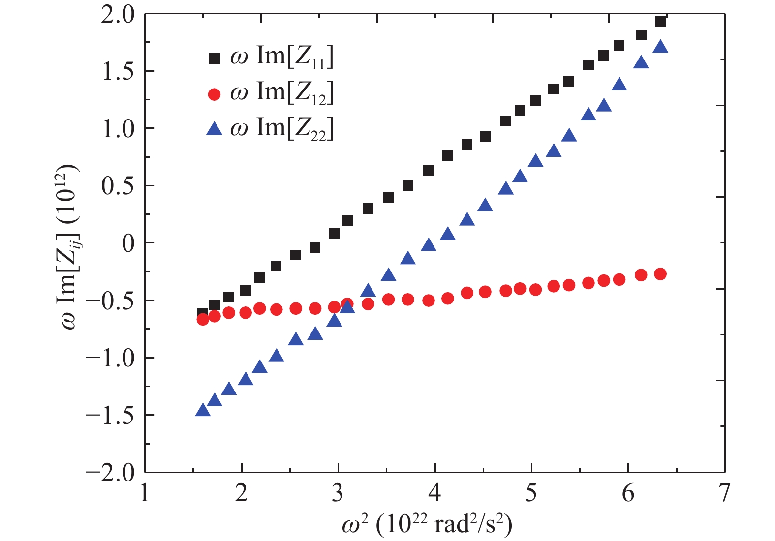
Fig. 6.  (Color online) Plot of ωIm(ωZij) versus ω2.

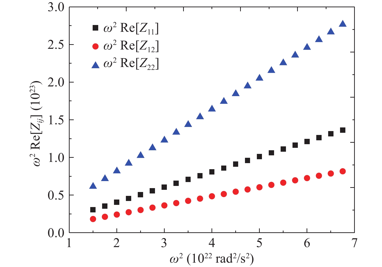
Fig. 7.  (Color online) Plot of ω2Re (Zij) versus ω2.

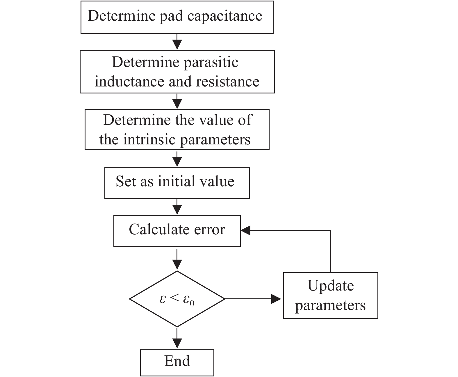
Fig. 8.  Flowchart for SSEC parameter extraction technique.

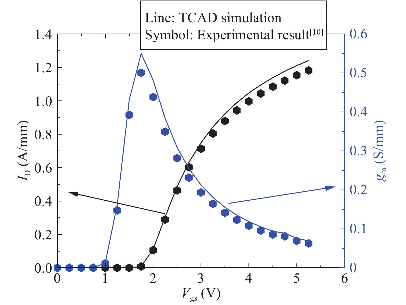
Fig. 9.  (Color online) Comparison of input transfer characteristics between TCAD simulation and experimental data[10] at Vds = 4 V.

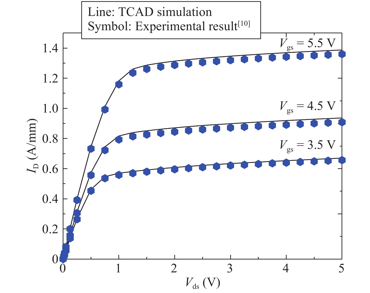
Fig. 10.  (Color online) Comparison of output characteristics between TCAD simulation and experimental data[10] for different gate voltages.

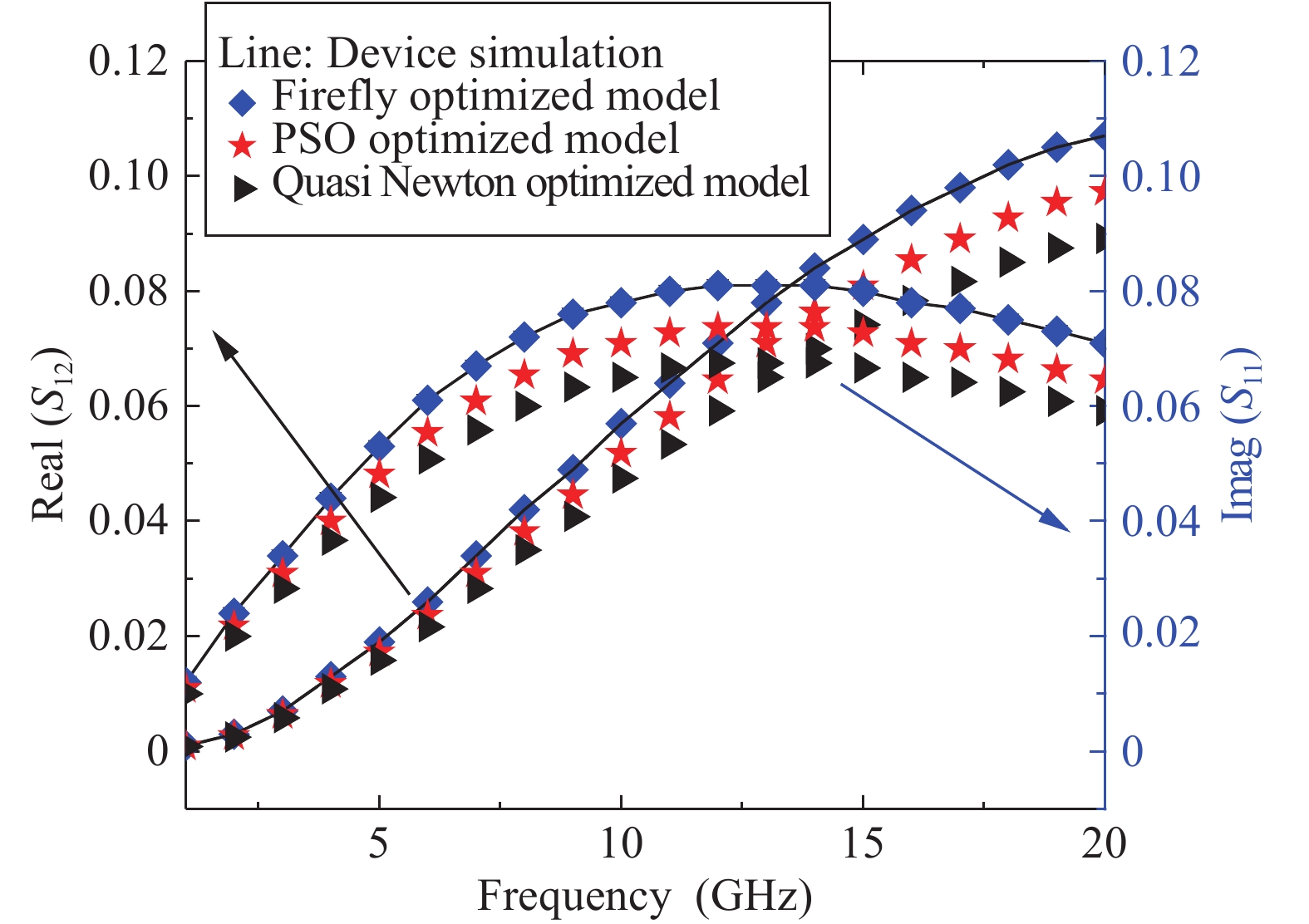
Fig. 12.  (Color online) Comparison of real and imaginary S12 versus different frequency for different optimization techniques.

Fig. 13.  (Color online) Comparison of real and imaginary S21 versus different frequency for different optimization techniques.

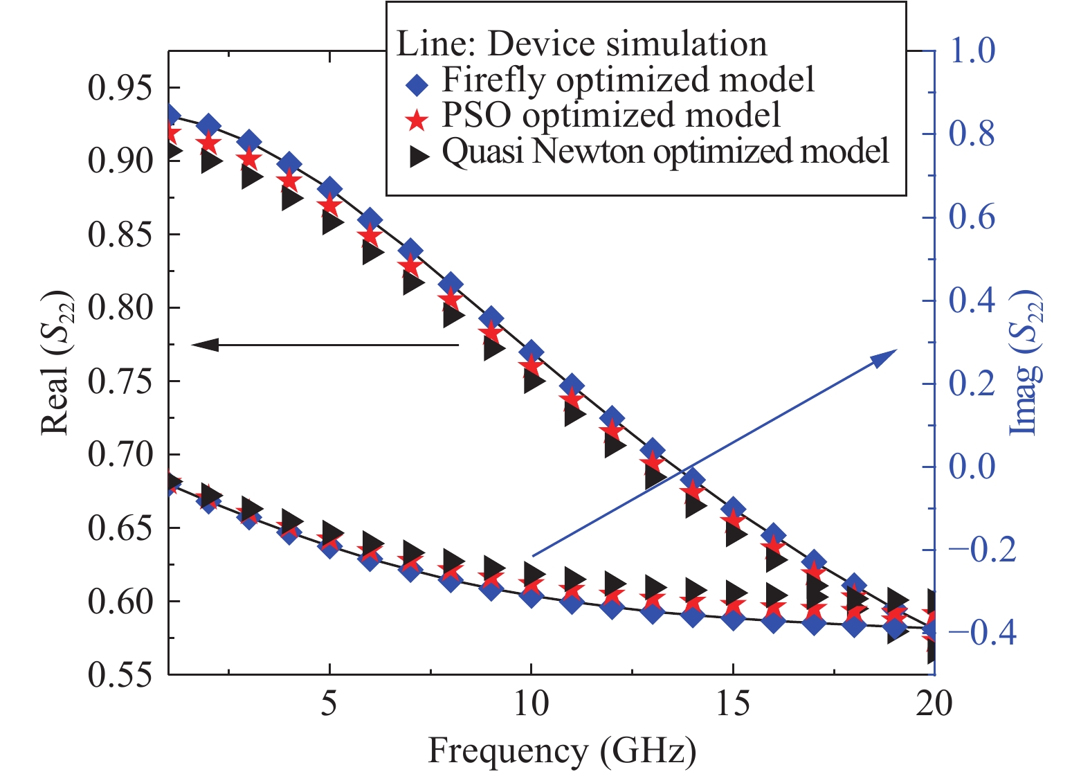
Fig. 14.  (Color online) Comparison of real and imaginary S22 versus different frequency for different optimization techniques.

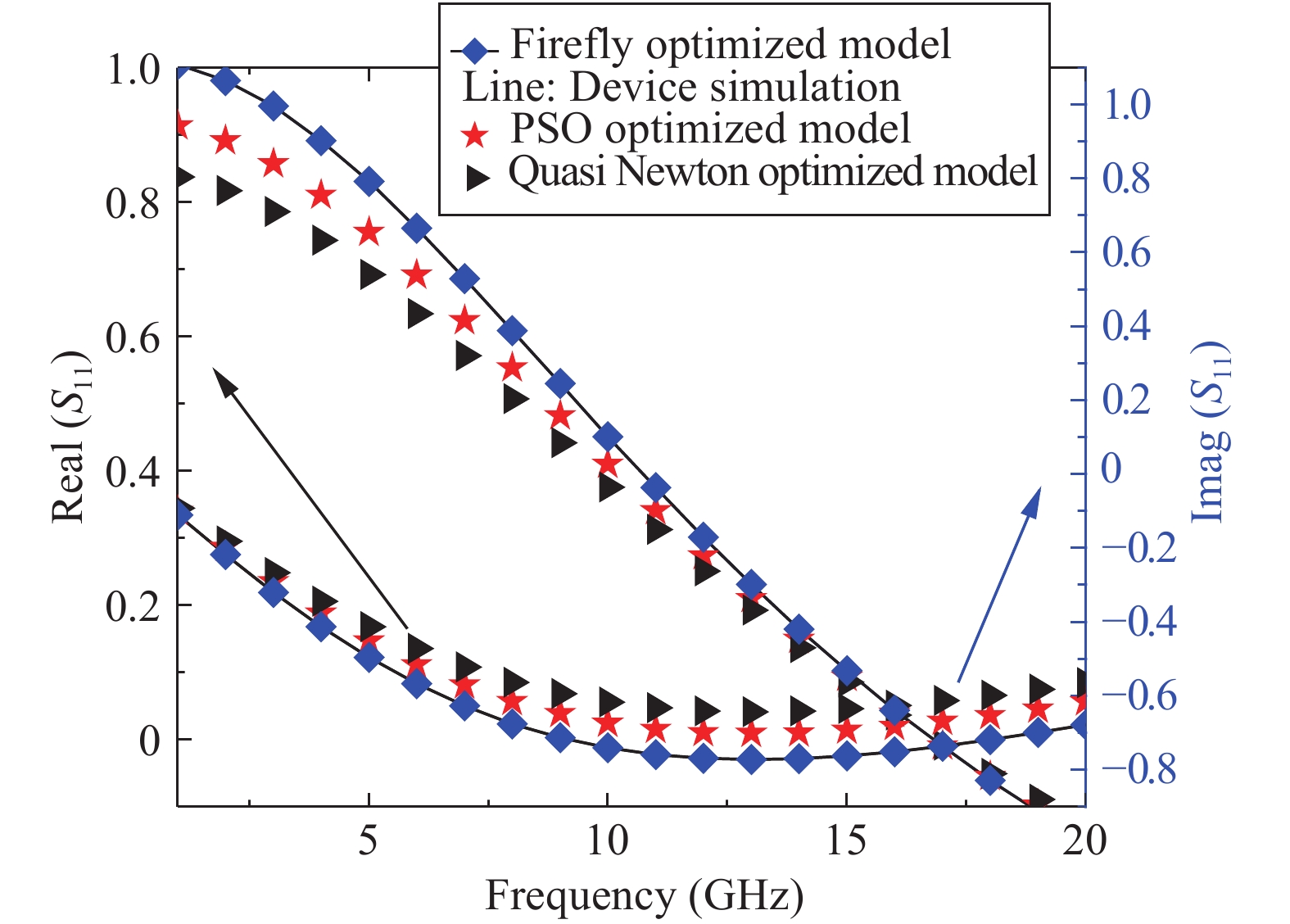
Fig. 11.  (Color online) Comparison of real and imaginary S11 versus different frequency for different optimization techniques.

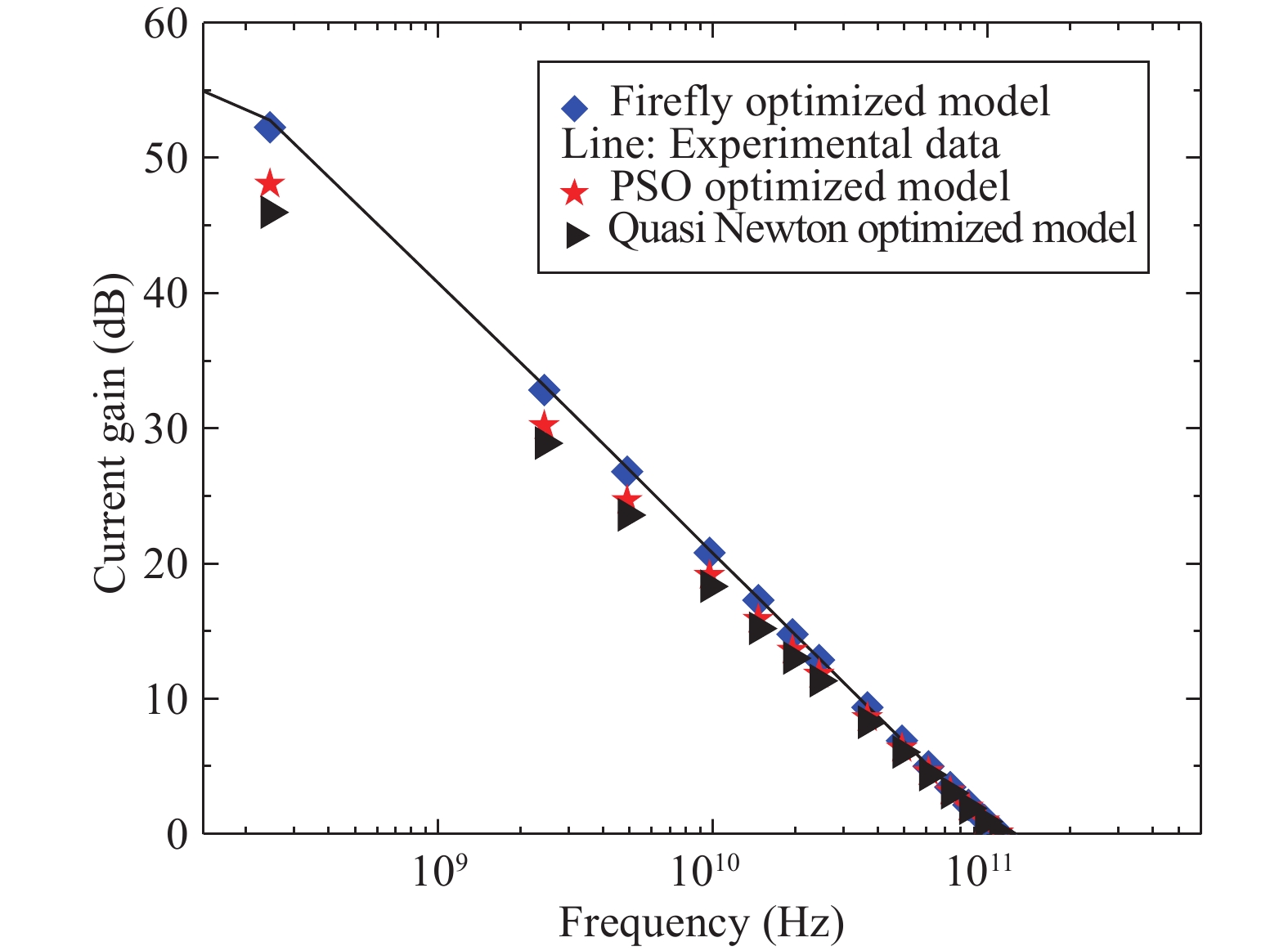
Fig. 15.  (Color online) Comparison of current gain versus different frequency for different optimization techniques and experimental data[10].

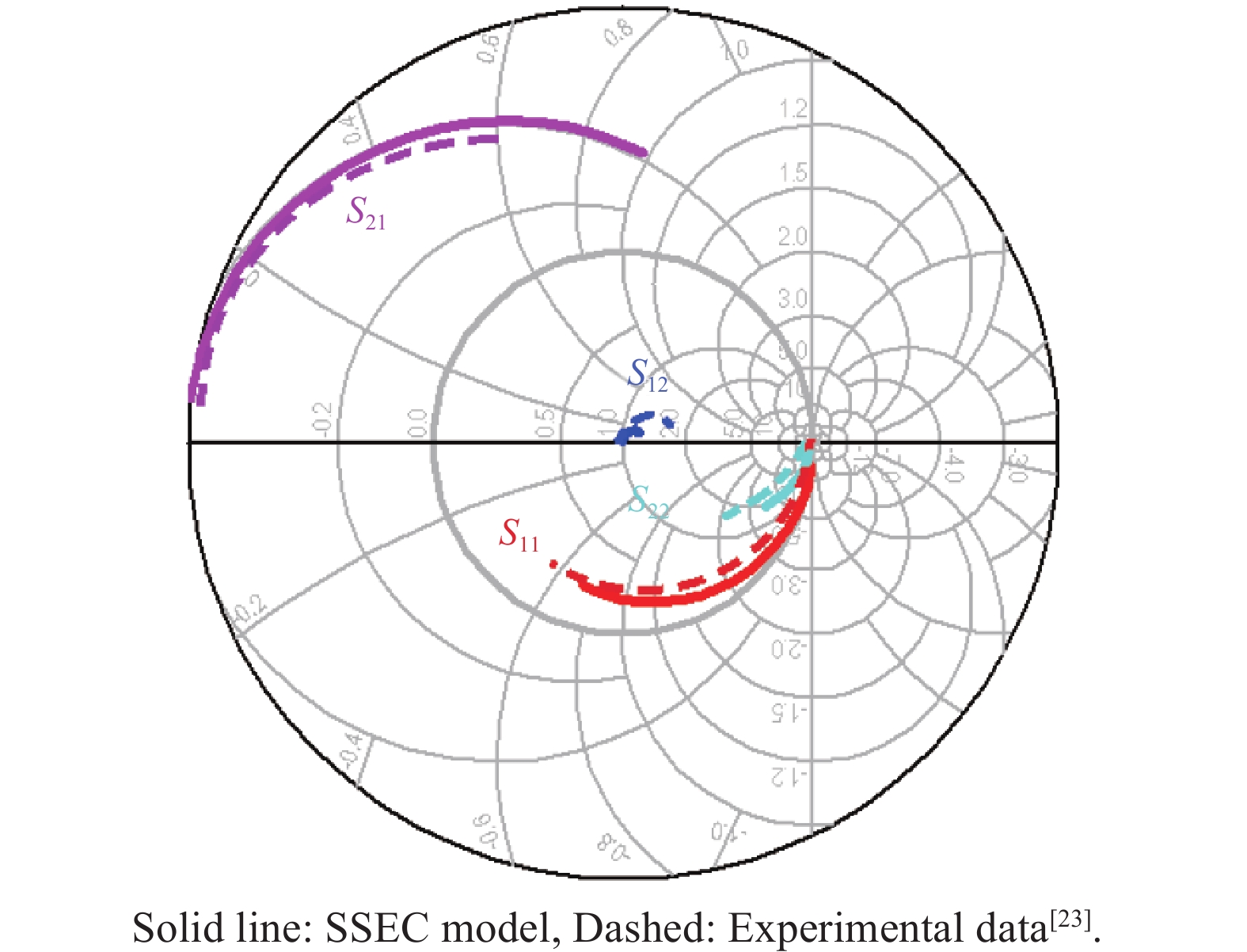
Fig. 16.  (Color online) Comparison of different S-parameters between Firefly optimized SSEC model and experimental data of 112 nm N-polar GaN MOS-HEMT[23] at Vds= 7 V, Vgs= 2 V at a frequency range of 1–20 GHz.

Table 1.   Extracted parameters with Firefly algorithm.

Parameter Initial value Search range (min) Search range (max) Firefly algorithm
Rs (Ω) 10 0 20 12
Rd (Ω) 28 0 30 26.395
Rg (Ω) 9 0 30 11.659
Ls (pH) 20 0 50 26
Ld (pH) 51 0 100 60
Lg (pH) 19 0 50 32
Cpd (fF) 44.46 10 100 36.892
Cpg (fF) 46.66 10 100 48.346
Cpgd (fF) 3.6 1 10 2.34
Cgs (fF) 46 1 100 84
Cgd (fF) 6.56 1 20 4.536
Cds (fF) 15 1 30 18
Rin (Ω) 4.33 1 10 2.5
Gm (mƱ) 550 400 600 486
Rgd (Ω) 80.092 10 200 76.98
gds (mS) 0.74 0 2 0.635
Τ (ps) 1.55 0.1 2 1.265
Ggs (mS) 0.235 0 2 0.156
Ggdf (mS) 0.000 09 0 1 0.000 97
DownLoad: CSV
[1]
Panda D K, Lenka T R. Modeling and simulation of enhancement mode p-GaN Gate AlGaN/GaN HEMT for RF circuit switch applications. J Semicond, 2017, 38(6): 064002 doi: 10.1088/1674-4926/38/6/064002
[2]
Panda D K, Lenka T R. Oxide thickness dependent compact model of channel noise for E-mode AlGaN/GaN MOS-HEMT. AEU - Int J Electron Commun, 2017, 82: 467 doi: 10.1016/j.aeue.2017.09.025
[3]
Jena K, Swain R, Lenka T R. Impact of barrier thickness on gate capacitance-modeling and comparative analysis of GaN based MOSHEMTs. J Semicond, 2015, 36(3): 034003 doi: 10.1088/1674-4926/36/3/034003
[4]
Panda D K, Lenka T R. Effects of trap density on drain current LFN and its model development for E-mode GaN MOS-HEMT. Superlattices Microstruct, 2017, 112: 374 doi: 10.1016/j.spmi.2017.09.045
[5]
Chen M. A 1–25 GHz GaN HEMT MMIC low-noise amplifier. IEEE Microwave Wireless Compon Lett, 20(10): 563
[6]
Sun H F, Alt A R, Benedickter H, et al. High-speed and low-noise AlInN/GaN HEMTs on SiC. Phys Status Solidi A, 2011, 208(2): 429 doi: 10.1002/pssa.201000518
[7]
Chen M Q, Sutton W, Smorchkova, et al. A 1–25 GHz GaN HEMT MMIC low-noise amplifier. IEEE Microwave Wireless Compon Lett, 2010, 20(10): 563 doi: 10.1109/LMWC.2010.2059002
[8]
Sun H F, Alt A R, Benedickter H, et al. Low-noise microwave performance of 0.1 μm gate AlInN/GaN HEMTs on SiC. IEEE Microwave Wireless Compon Lett, 2010, 20(8): 453 doi: 10.1109/LMWC.2010.2049008
[9]
Li B, Wei L, Wen C. Static characteristics and short channel effect in enhancement-mode AlN/GaN/AlN N-polar MISFET with self-aligned source/drain regions. J Semicond, 2014, 35(12): 124006 doi: 10.1088/1674-4926/35/12/124006
[10]
Singisetti U, Wong M H, Speck J S, et al. Enhancement-mode N-polar GaN MOS-HFET with 5-nm GaN channel, 510-mS/mm gm, and 0.66- ohm·mm Ron’. IEEE Electron Device Lett, 2012, 33(1): 6 doi: 10.1109/LED.2011.2178050
[11]
Essaadali R, Jarndal A, Kouki A B, et al. A new GaN HEMT equivalent circuit modeling technique based on X-parameters. IEEE Trans Microwave Theory Tech, 2016, 64(9): 2758 doi: 10.1109/TMTT.2016.2594234
[12]
Alt A R, Marti D, Bolognesi C R. Transistor modeling: robust small-signal equivalent circuit extraction in various HEMT technologies. IEEE Microwave Mag, 2013, 14(4): 83 doi: 10.1109/MMM.2013.2248593
[13]
Du J, Xu P, Wang K, et al. Small-signal modeling of AlGaN/GaN HEMTs with consideration of CPW capacitances. J Semicond, 2015, 36(3): 34009 doi: 10.1088/1674-4926/36/3/034009
[14]
Crupi G, Schreurs D M M P, Caddemi A, et al. High-frequency extraction of the extrinsic capacitances for GaN HEMT technology. IEEE Microwave Wireless Compon Lett, 2011, 21(8): 445 doi: 10.1109/LMWC.2011.2160525
[15]
Resca D, Raffo A, Santarelli A, et al. Scalable equivalent circuit FET model for MMIC design identified through FW-EM analyses. IEEE Trans Microwave Theory Tech, 2009, 57(2): 245 doi: 10.1109/TMTT.2008.2011208
[16]
Snowden C M. Large-signal microwave characterization of AlGaAs/GaAs HBT's based on a physics-based electrothermal model. IEEE Trans Microwave Theory Tech, 1997, 45(1): 58 doi: 10.1109/22.552033
[17]
Majumdar A, Chatterjee S, Chatterjee S, et al. Optimization of intrinsic elements from small-signalmodel of GaN HEMT by using PSO. IEEE Applied Electromagnetics Conference (AEMC), Guwahati, 2015: . 1
[18]
Kumar R, Rajan A, Talukdar F A, et al. Optimization of 5.5-GHz CMOS LNA parameters using firefly algorithm. Neural Computing and Applications, 2016: 1
[19]
Brady R G, Oxley C H, Brazil T J. An improved small-signal parameter-extraction algorithm for GaN HEMT devices. IEEE Trans Microwave Theory Tech, 2008, 56(7): 1535 doi: 10.1109/TMTT.2008.925212
[20]
Dambrine G, Cappy A, Heliodore F, et al. A new method for determining the FET small-signal equivalent circuit. IEEE Trans Microwave Theory Tech, 1988, 36(7): 1151 doi: 10.1109/22.3650
[21]
Jarndal A, Kompa G. A new small-signal modeling approach applied to GaN devices. IEEE Trans Microwave Theory Tech, 2005, 53(11): 3440 doi: 10.1109/TMTT.2005.857332
[22]
Yanagawa S, Ishihara H, Ohtomo M. Analytical method for determining equivalent circuit parameters of GaAs FETs. IEEE Trans Microwave Theory Tech, 1996, 44(10): 1637 doi: 10.1109/22.538954
[23]
Nidhi, Dasgupta S, Keller S, et al. N-Polar GaN/AlN MIS-HEMT with fMAX of 204 GHz for Ka-band applications. IEEE Electron Device Lett, 2011, 32(12): 1683 doi: 10.1109/LED.2011.2168558
  • Search

    Advanced Search >>

    GET CITATION

    shu

    Export: BibTex EndNote

    Article Metrics

    Article views: 4022 Times PDF downloads: 80 Times Cited by: 0 Times

    History

    Received: 06 June 2017 Revised: 20 November 2017 Online: Accepted Manuscript: 04 April 2018Uncorrected proof: 12 April 2018Published: 01 July 2018

    Catalog

      Email This Article

      User name:
      Email:*请输入正确邮箱
      Code:*验证码错误
      D. K. Panda, G. Amarnath, T. R. Lenka. Small-signal model parameter extraction of E-mode N-polar GaN MOS-HEMT using optimization algorithms and its comparison[J]. Journal of Semiconductors, 2018, 39(7): 074001. doi: 10.1088/1674-4926/39/7/074001 ****D K Panda, G Amarnath, T R Lenka, Small-signal model parameter extraction of E-mode N-polar GaN MOS-HEMT using optimization algorithms and its comparison[J]. J. Semicond., 2018, 39(7): 074001. doi: 10.1088/1674-4926/39/7/074001.
      Citation:
      D. K. Panda, G. Amarnath, T. R. Lenka. Small-signal model parameter extraction of E-mode N-polar GaN MOS-HEMT using optimization algorithms and its comparison[J]. Journal of Semiconductors, 2018, 39(7): 074001. doi: 10.1088/1674-4926/39/7/074001 ****
      D K Panda, G Amarnath, T R Lenka, Small-signal model parameter extraction of E-mode N-polar GaN MOS-HEMT using optimization algorithms and its comparison[J]. J. Semicond., 2018, 39(7): 074001. doi: 10.1088/1674-4926/39/7/074001.

      Small-signal model parameter extraction of E-mode N-polar GaN MOS-HEMT using optimization algorithms and its comparison

      doi: 10.1088/1674-4926/39/7/074001
      More Information
      • Corresponding author: E-mail: t.r.lenka@ieee.org
      • Received Date: 2017-06-06
      • Revised Date: 2017-11-20
      • Published Date: 2018-07-01

      Catalog

        /

        DownLoad:  Full-Size Img  PowerPoint
        Return
        Return