J. Semicond. > 2018, Volume 39 > Issue 7 > 074004

SEMICONDUCTOR DEVICES

A GaN/InGaN/AlGaN MQW RTD for versatile MVL applications with improved logic stability

Haipeng Zhang1, Qiang Zhang1, , Mi Lin1, Weifeng Lü1, Zhonghai Zhang1, Jianling Bai1, Jian He1, Bin Wang1 and Dejun Wang2

+ Author Affiliations

 Corresponding author: Qiang Zhang, Email: 1446837801@qq.com

DOI: 10.1088/1674-4926/39/7/074004

PDF

Turn off MathJax

Abstract: To improve the logic stability of conventional multi-valued logic (MVL) circuits designed with a GaN-based resonate tunneling diode (RTD), we proposed a GaN/InGaN/AlGaN multi-quantum well (MQW) RTD. The proposed RTD was simulated through solving the coupled Schrodinger and Poisson equations in the numerical non-equilibrium Green’s function (NEGF) method on the TCAD platform. The proposed RTD was grown layer by layer in epitaxial technologies. Simulated results indicate that its current-voltage characteristic appears to have a wider total negative differential resistance region than those of conventional ones and an obvious hysteresis loop at room temperature. To increase the Al composite of AlGaN barrier layers properly results in increasing of both the total negative differential resistance region width and the hysteresis loop width, which is helpful to improve the logic stability of MVL circuits. Moreover, the complement resonate tunneling transistor pair consisted of the proposed RTDs or the proposed RTD and enhanced mode HEMT controlled RTD is capable of generating versatile MVL modes at different supply voltages less than 3.3 V, which is very attractive for implementing more complex MVL function digital integrated circuits and systems with less devices, super high speed linear or nonlinear ADC and voltage sensors with a built-in super high speed ADC function.

Key words: GaN/InGaN/AlGaNMQWRTDtotal NDR region widthhysteresis characteristicMVL


[1]
Ambacher O, Smart J, Shealy J R, et al. Two-dimensional electron gases induced by spontaneous and piezoelectric polarization charges in N- and Ga-face AlGaN/GaN heterostructures. J Appl Phys, 1999, 85(1): 3222 doi: 10.1063/1.369664
[2]
Fiorentini V, Bernardini F, Ambacher O. Evidence for nonlinear macroscopic polarization in III–V nitride alloy heterostructures. Appl Phys Lett, 2002, 80(7): 1204 doi: 10.1063/1.1448668
[3]
Chowdhury S, Biswas D. Performances comparison of Si, GaAs and GaN based resonant tunneling diode in presence and absence of electric field. IJ-Nano, 2012, 1(2): 39 doi: 10.11591/ij-nano.v1i2.1324
[4]
Yahyaoui N, Sfina N, Nasrallah S A, et al. Electron transport through cubic InGaN/AlGaN resonant tunneling diodes. Comput Phys Commun, 2014, 185(12): 3119 doi: 10.1016/j.cpc.2014.08.006
[5]
Chowdhury S, Chattaraj S, Biswas D. Design and simulation of a novel GaN based resonant tunneling high electron mobility transistor on a silicon substrate. J Semicond, 2015, 36(4): 044001 doi: 10.1088/1674-4926/36/4/044001
[6]
Zhang H P, Ning X, Lin M, et al. A GaAs/AlGaAs based asymmetrical DBS (ADBS) RTD. Proc of the 2015 International Conference on Communication Technology, 2015: 380 doi: 10.1109/ICCT.2015.7399862
[7]
Rached A, Bhouri A, Sakr S, et al. Self-consistent vertical transport calculations in AlxGa1-xN/GaN based resonant tunneling diode. Superlattices Microstruct, 2016, 91: 37 doi: 10.1016/j.spmi.2015.12.035
[8]
Sankaranarayanan S, Saha D. Giant peak to valley ratio in a GaN based resonant tunnel diode with barrier width modulation. Superlattices Microstruct, 2016, 98: 174 doi: 10.1016/j.spmi.2016.08.017
[9]
Singh M M, Siddiqui M J. Electrical characterization of triple barrier GaAs/AlGaAs RTD with dependence of operating temperature and barrier lengths. Mater Sci Semicond Process, 2017, 58: 89 doi: 10.1016/j.mssp.2016.10.014
[10]
Zhang H P, Hao X L, Lin M, et al. A Restrain Method of Polarization Effect in GaN/AlGaN RTD. Adv Comput Sci Res, 2017, 58: 169 doi: 10.2991/msota-16.2016.39
[11]
Zubialevich V Z, Rzheutski M V, Li H, et al. InxAl1–xN/Al0.53Ga0.47N multiple quantum wells on Al0.5Ga0.5N buffer with variable in-plane lattice parameter. J Lumin, 2018, 194: 797 doi: 10.1016/j.jlumin.2017.09.053
[12]
Sandeep S, Swaroop G, Dipankar S. Polarization modulation in GaN-based double-barrier resonant tunneling diodes. Appl Phys Express, 2014, 7(9): 095201 doi: 10.7567/APEX.7.095201
[13]
Xiang W, Wang G, Hao H, et al. InAs homoepitaxy and InAs/AlSb/GaSb resonat interband tunneling diodes on inas substrate. J Cryst Growth, 2016, 443(1): 85 doi: 10.1016/j.jcrysgro.2016.03.021
[14]
Monozon B S, Schmelcher P. Fine structure of the exciton electroabsorption in semiconductor superlattices. Physica B, 2017, 507: 61 doi: 10.1016/j.physb.2016.11.017
[15]
Kumar V, Sinha A, Singh B P, et al. Second-order nonlinear optical susceptibilities of AIIBVI and AIIIBV semiconductors. Phys Lett A, 2016, 380: 3630 doi: 10.1016/j.physleta.2016.09.006
[16]
Wang Q, Gao X, Xu Y, et al. Carrier localization in strong phase-separated InGaN/GaN multiple-quantum-well dual-wavelength LEDs. J Alloys Compounds, 2017, 726: 460 doi: 10.1016/j.jallcom.2017.07.326
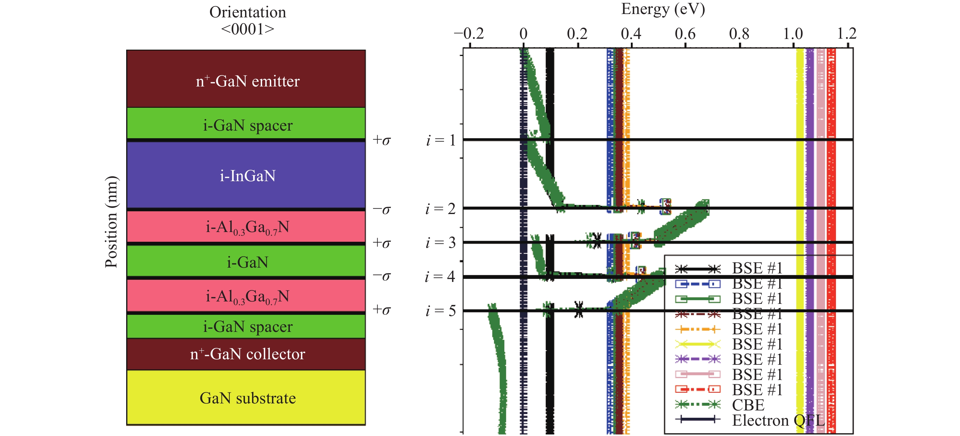
Fig. 1.  (Color online) Cross-section view, interface polarization charge density and bound states distributions of the proposed GaN/InGaN/ AlGaN MQW RTD.

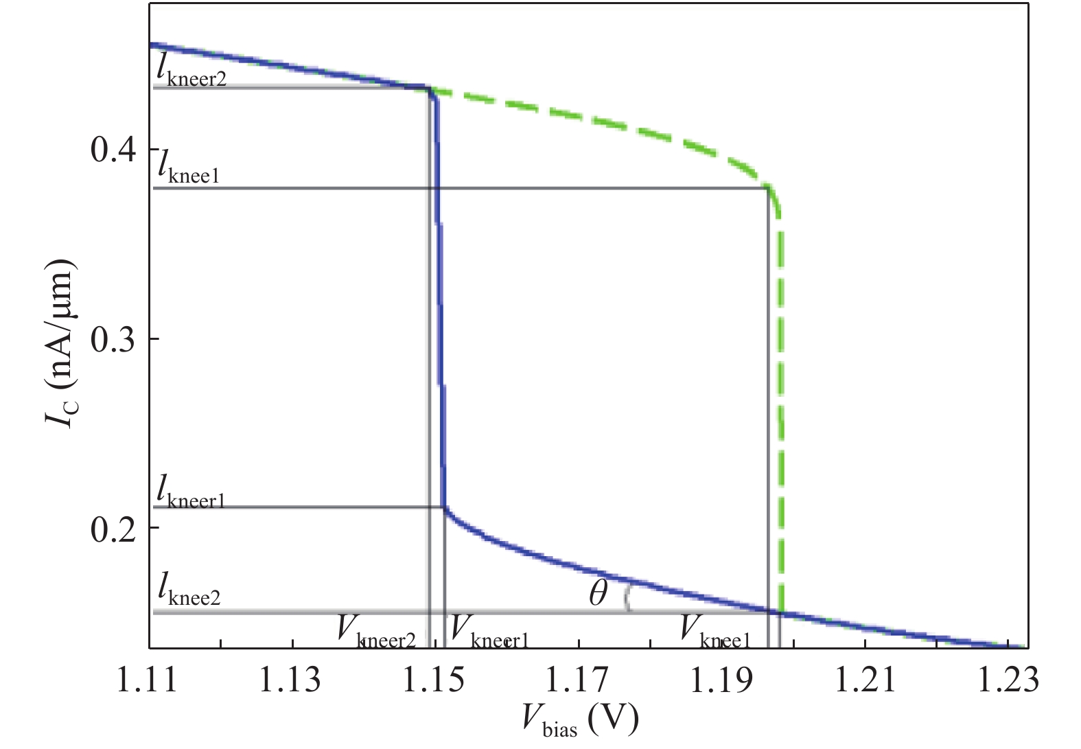
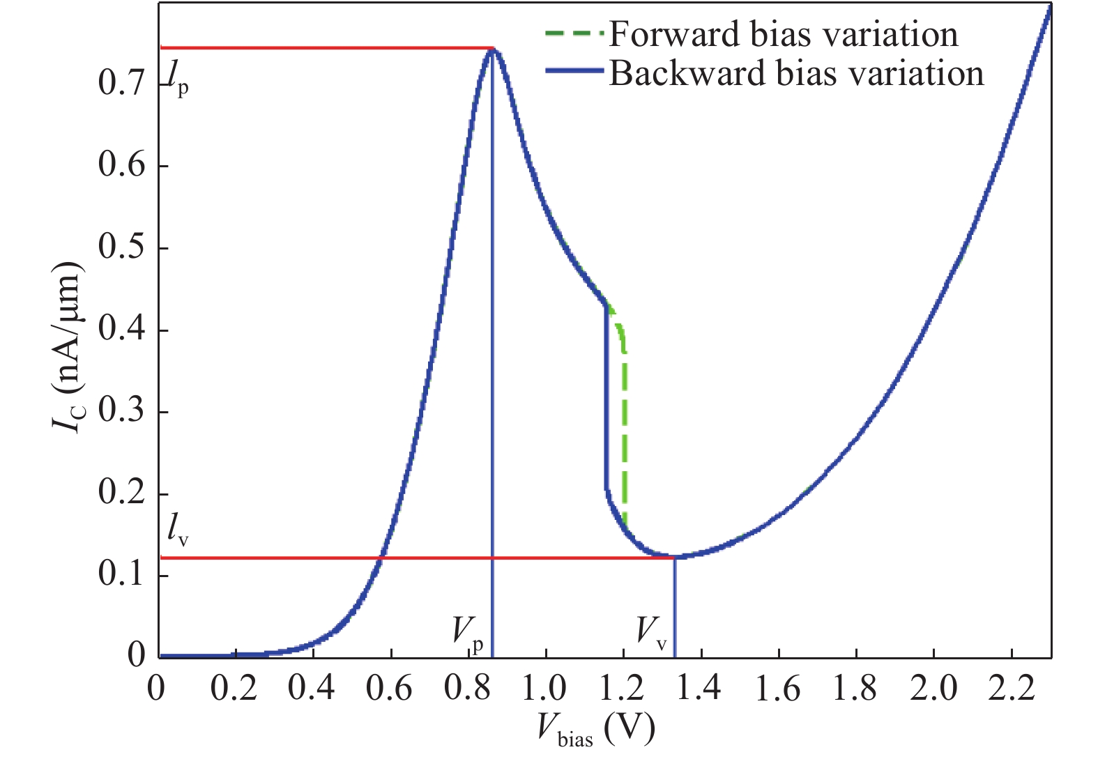
Fig. 3.  (Color online) Key parameters definition of hysteresis loop in Fig. 2.

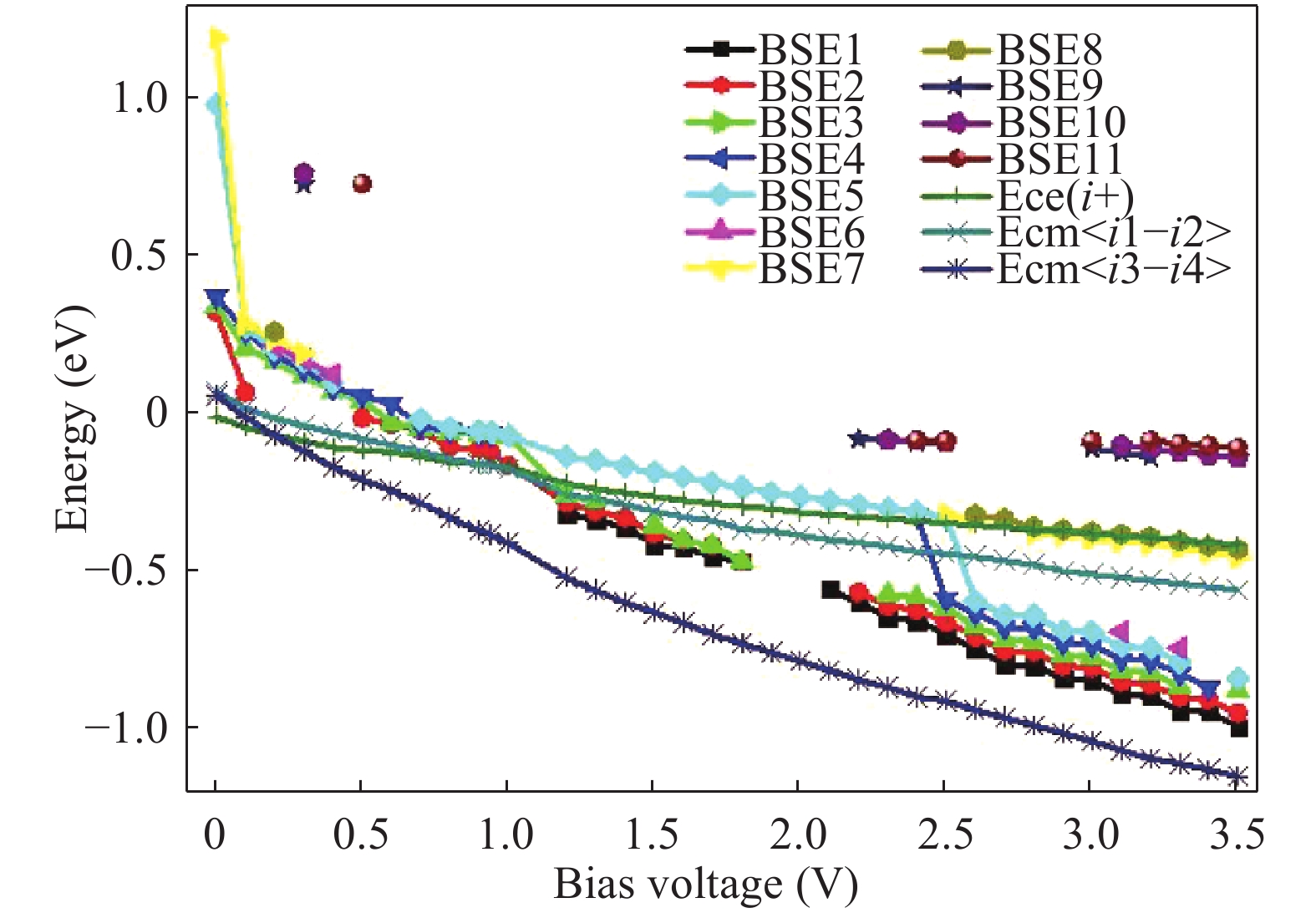
Fig. 4.  (Color online) Separation, degeneration and jumping of the BSE levels vs. bias voltage.

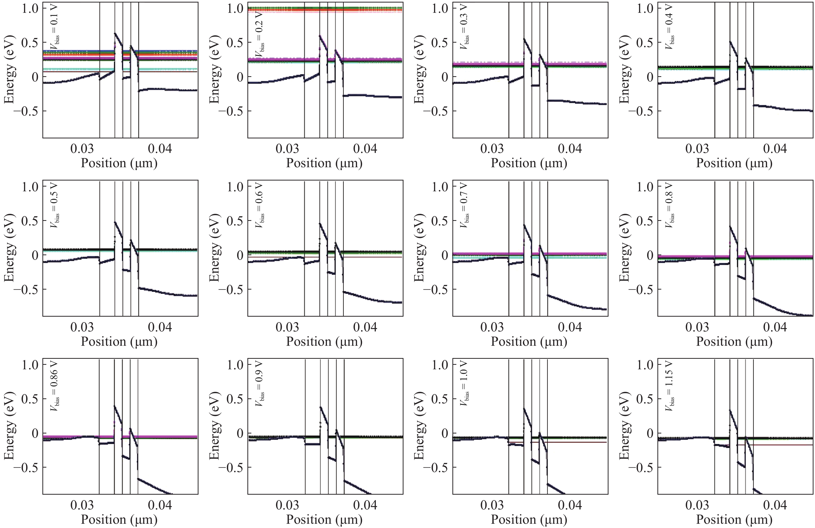
Fig. 5.  (Color online) The BSE distribution of the proposed GaN/InGaN/AlGaN MQW RTD.

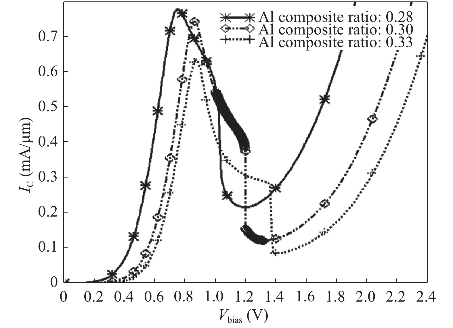
Fig. 6.  Influence of Al composite ratio on current–voltage characteristic of the proposed RTD.

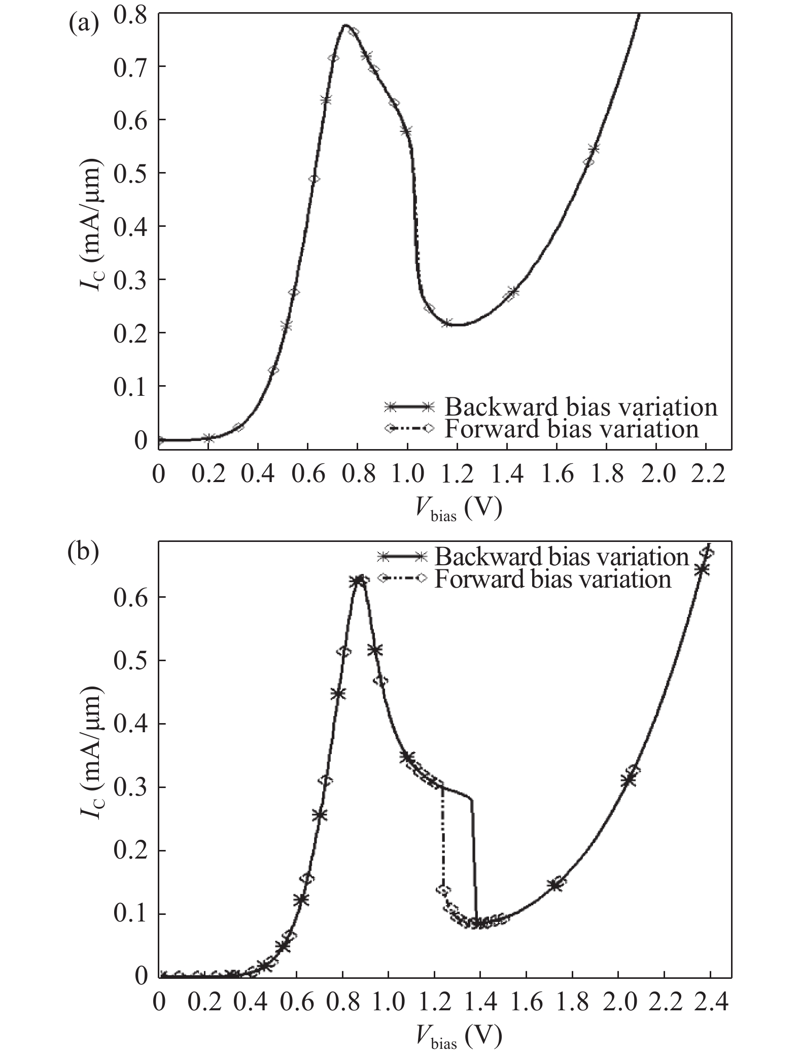
Fig. 7.  Influence of Al composite ratio on the hysteresis characteristic of the proposed RTD. (a) Al composite ratio at 0.28. (b) Al composite ratio at 0.33.

Fig. 2.  (Color online) Current–voltage curve of the proposed RTD.

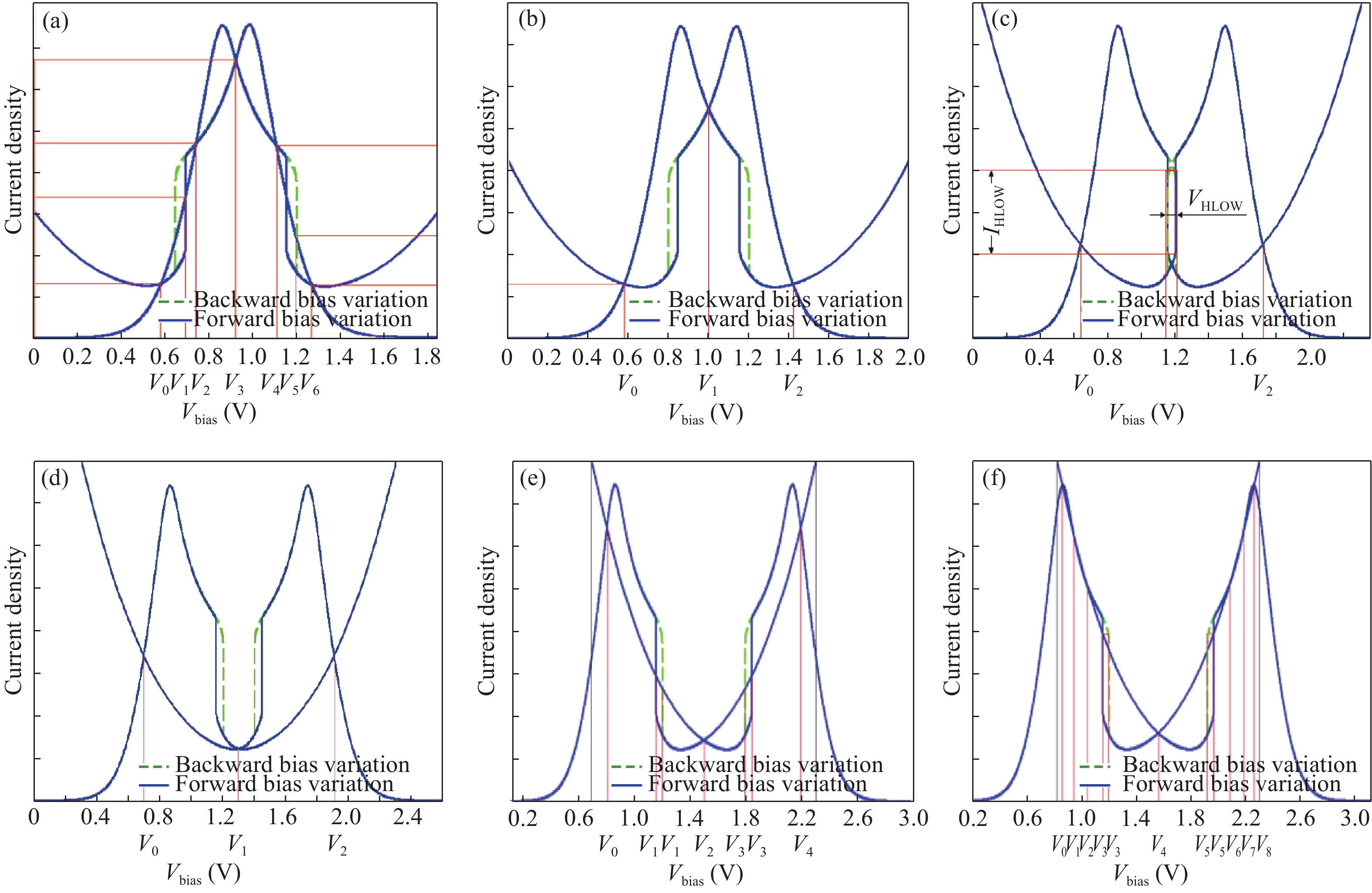
Fig. 8.  (Color online) Possible MVL provided by the complement RTD pair with the proposed GaN-based RTD at different supply voltage. (a) 7-valued logic levels at about 1.84 V supply voltage. (b) 3-valued logic levels at about 2.0 V supply voltage. (c) 3-valued logic levels with different middle logic values at the window edges of hysteresis loop at about 2.35 V supply voltage. (d) 3-valued logic levels at about 2.6 V supply voltage. (e) 5-valued logic levels at about 3.0 V supply voltage. (f) 9-valued logic levels at about 3.1 V supply voltage.

Fig. 9.  (Color online) Flexible MVL characteristics of the proposed complement GaN/InGaN/AlGaN MQW RTD pair with its barrier layer Al composite ratio at 0.28. (a) 7-valued logic levels at about 1.62 V supply voltage. (b) 3-valued logic levels at about 2.3 V supply voltage. (c) 3-valued logic levels at about 2.6 V supply voltage.

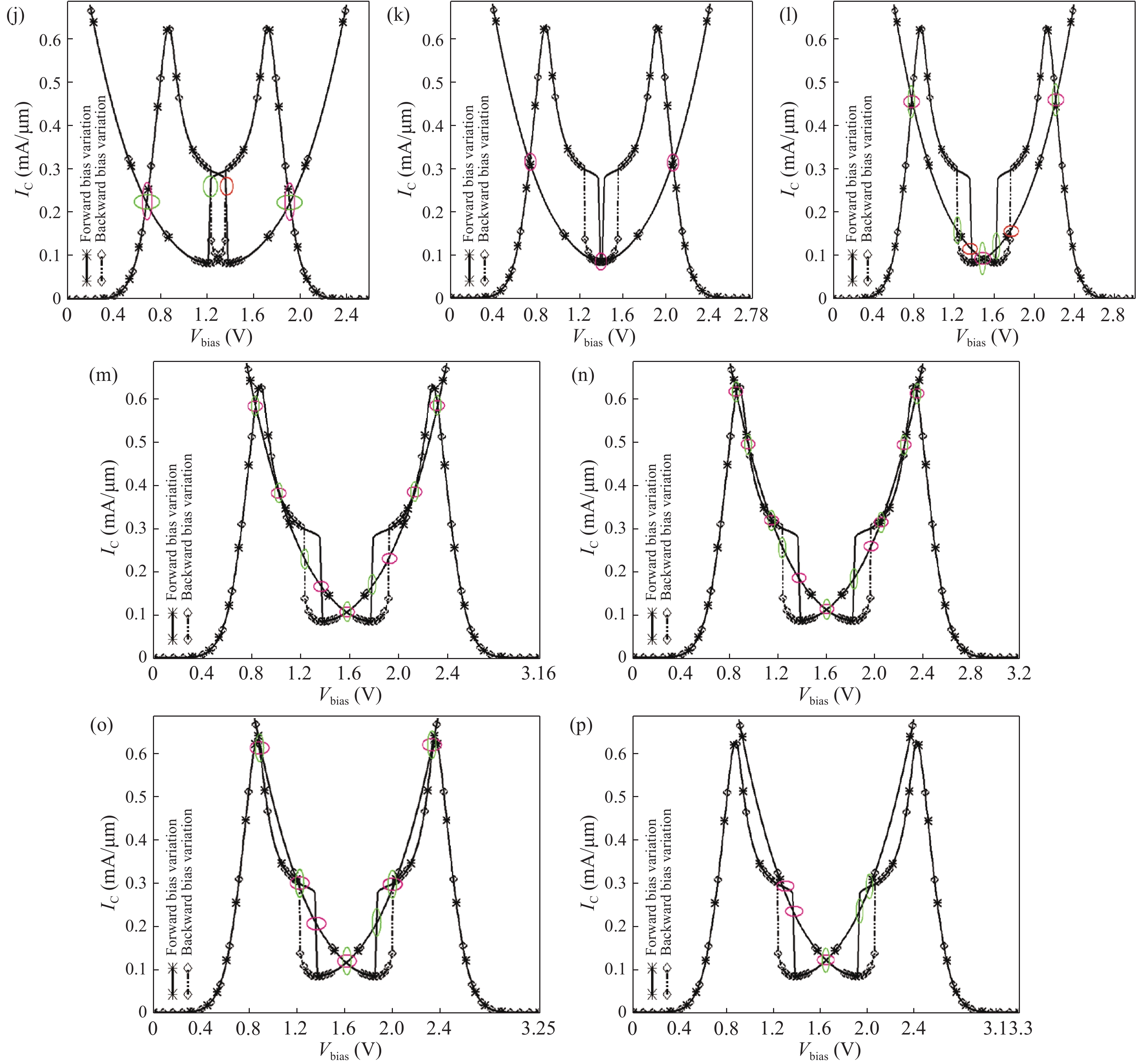
Fig. 10.  (Color online) Flexible MVL characteristics of the proposed complement GaN/InGaN/AlGaN MQW RTD pair with its barrier layer Al composite ratio at 0.33 (outlined in Table 2). (a) Tangle peak. (b) Low normal 3-value-logic. (c) Edge $\left\langle {2|1} \right\rangle $ 4-value-logic. (d) Edge $\left\langle {3|1} \right\rangle $ 5-value-logic. (e) Edge $\left\langle {2|2} \right\rangle $ 5-value-logic. (f) Edge $\left\langle {1|3} \right\rangle $ 5-value-logic. (g) Edge $\left\langle {1|2} \right\rangle $ 4-value-logic. (h) Middle normal 3-value-logic. (i) Critical middle normal 3-value-logic. (j) Edge $\left\langle {1|2} \right\rangle $ 3-value-logic. (k) Critical edge $\left\langle {1|2} \right\rangle $ 3-value-logic. (l) Edge $\left\langle {2|2} \right\rangle $ 5-value-logic. (m) Edge $\left\langle {3|3} \right\rangle $ 7-value-logic. (n) Edge $\left\langle {4|4} \right\rangle $ 9-value-logic. (o) Edge $\left\langle {3|2} \right\rangle $ 6-value-logic. (p) Edge $\left\langle {2|0} \right\rangle $ 3-value-logic.

Table 1.   Thickness of each layer.

Region Thickness (nm)
n+-GaN emitter 62
i-GaN spacer 3.0
i-In0.03Ga0.97N 2.0
i-Al0.3Ga0.7N 1.0
i-GaN 1.0
i-Al0.3Ga0.7N 1.0
i-GaN spacer 3.0
n+-GaN collector 62
DownLoad: CSV

Table 2.   The flexible MVL characteristics of the proposed complement RTD pair with its barrier layer Al composite ratio at 0.33.

Graph order in Fig. 10 Type of MVLs Supply voltage scope (V) Logic voltage scope (V) Logic stability
(a) Tangle peak 1.75 [0.79, 0.97] unstable
(b) Low normal 3-value-logic 1.75–1.86 (0.73,0.79), (0.875,0.93), (0.97,1.13) stable
(c) Edge $\left\langle {2|1} \right\rangle $ 4-value-logic 1.86 P:0.62, 0.73, 0.93, 1.12, N:1.23 unstable
(d) Edge $\left\langle {3|1} \right\rangle $ 5-value-logic 1.86–1.96 P:(0.59,0.62),P:(0.62,0.71),(0.71,0.73),(0.93,0.98), N:(1.12,1.23),N:(1.23,1.37) stable
(e) Edge $\left\langle {2|2} \right\rangle $ 5-value-logic 1.96 0.59, N:0.71, 0.98, P:1.23, 1.37 unstable
(f) Edge $\left\langle {1|3} \right\rangle $ 5-value-logic 1.96–2.08 (0.59,0.60), N:(0.70,0.71), (0.98,1.04),P:(1.23,1.37), (1.38,1.47) stable
(g) Edge $\left\langle {1|2} \right\rangle $ 4-value-logic 2.08 0.60, N:0.70, 1.04, P:1.37, 1.47 unstable
(h) and (i) top normal 3-value-logic 2.08–2.46 (0.60,0.66], (1.04,1.23], (1.47,1.82] stable
(i), (j) and (k) Edge $\left\langle {1|2} \right\rangle $ 3-value-logic 2.46–2.78 [0.66, 0.73], N/P:[1.23, 1.39], [1.82, 2.05] stable
(l) Edge $\left\langle {2|2} \right\rangle $ 5-value-logic 2.78–3.16 (0.73,0.83), N:1.23, P:1.37, (1.39,1.58),N:(1.39,1.78), P:(1.39,1.91), (2.05,2.32) stable
(m) Edge $\left\langle {3|3} \right\rangle $ 7-value-logic 3.16 0.83,1.04, N:1.23, P:1.37, 1.58,N:1.78, P:1.91, 2.17,2.32 unstable
(n) Edge $\left\langle {4|4} \right\rangle $ 9-value-logic 3.16–3.25 (0.83,0.87), (0.87,1.04), (1.04,1.23), N:1.23P:1.37, (1.58,1.645), N:(1.78,1.88), P:(1.91,2.06), (2.06,2.17), (2.17,2.31), (2.31,2.32) stable
(o) Edge $\left\langle {3|2} \right\rangle $ 6-value-logic 3.25 0.87, 1.23, P:1.37, 1.645, N:1.88, 2.06, 2.31 unstable
(p) Edge $\left\langle {2|0} \right\rangle $ 3-value-logic 3.25–3.38 P:(1.23,1.36), P:(1.36,1.37), (1.645,1.69),N:(1.88,1.98), N:(1.98,2.06) stable
_ Edge $\left\langle {1|0} \right\rangle $ 2-value-logic 3.38 P:1.36, 1.69, N:1.98 unstable
DownLoad: CSV
[1]
Ambacher O, Smart J, Shealy J R, et al. Two-dimensional electron gases induced by spontaneous and piezoelectric polarization charges in N- and Ga-face AlGaN/GaN heterostructures. J Appl Phys, 1999, 85(1): 3222 doi: 10.1063/1.369664
[2]
Fiorentini V, Bernardini F, Ambacher O. Evidence for nonlinear macroscopic polarization in III–V nitride alloy heterostructures. Appl Phys Lett, 2002, 80(7): 1204 doi: 10.1063/1.1448668
[3]
Chowdhury S, Biswas D. Performances comparison of Si, GaAs and GaN based resonant tunneling diode in presence and absence of electric field. IJ-Nano, 2012, 1(2): 39 doi: 10.11591/ij-nano.v1i2.1324
[4]
Yahyaoui N, Sfina N, Nasrallah S A, et al. Electron transport through cubic InGaN/AlGaN resonant tunneling diodes. Comput Phys Commun, 2014, 185(12): 3119 doi: 10.1016/j.cpc.2014.08.006
[5]
Chowdhury S, Chattaraj S, Biswas D. Design and simulation of a novel GaN based resonant tunneling high electron mobility transistor on a silicon substrate. J Semicond, 2015, 36(4): 044001 doi: 10.1088/1674-4926/36/4/044001
[6]
Zhang H P, Ning X, Lin M, et al. A GaAs/AlGaAs based asymmetrical DBS (ADBS) RTD. Proc of the 2015 International Conference on Communication Technology, 2015: 380 doi: 10.1109/ICCT.2015.7399862
[7]
Rached A, Bhouri A, Sakr S, et al. Self-consistent vertical transport calculations in AlxGa1-xN/GaN based resonant tunneling diode. Superlattices Microstruct, 2016, 91: 37 doi: 10.1016/j.spmi.2015.12.035
[8]
Sankaranarayanan S, Saha D. Giant peak to valley ratio in a GaN based resonant tunnel diode with barrier width modulation. Superlattices Microstruct, 2016, 98: 174 doi: 10.1016/j.spmi.2016.08.017
[9]
Singh M M, Siddiqui M J. Electrical characterization of triple barrier GaAs/AlGaAs RTD with dependence of operating temperature and barrier lengths. Mater Sci Semicond Process, 2017, 58: 89 doi: 10.1016/j.mssp.2016.10.014
[10]
Zhang H P, Hao X L, Lin M, et al. A Restrain Method of Polarization Effect in GaN/AlGaN RTD. Adv Comput Sci Res, 2017, 58: 169 doi: 10.2991/msota-16.2016.39
[11]
Zubialevich V Z, Rzheutski M V, Li H, et al. InxAl1–xN/Al0.53Ga0.47N multiple quantum wells on Al0.5Ga0.5N buffer with variable in-plane lattice parameter. J Lumin, 2018, 194: 797 doi: 10.1016/j.jlumin.2017.09.053
[12]
Sandeep S, Swaroop G, Dipankar S. Polarization modulation in GaN-based double-barrier resonant tunneling diodes. Appl Phys Express, 2014, 7(9): 095201 doi: 10.7567/APEX.7.095201
[13]
Xiang W, Wang G, Hao H, et al. InAs homoepitaxy and InAs/AlSb/GaSb resonat interband tunneling diodes on inas substrate. J Cryst Growth, 2016, 443(1): 85 doi: 10.1016/j.jcrysgro.2016.03.021
[14]
Monozon B S, Schmelcher P. Fine structure of the exciton electroabsorption in semiconductor superlattices. Physica B, 2017, 507: 61 doi: 10.1016/j.physb.2016.11.017
[15]
Kumar V, Sinha A, Singh B P, et al. Second-order nonlinear optical susceptibilities of AIIBVI and AIIIBV semiconductors. Phys Lett A, 2016, 380: 3630 doi: 10.1016/j.physleta.2016.09.006
[16]
Wang Q, Gao X, Xu Y, et al. Carrier localization in strong phase-separated InGaN/GaN multiple-quantum-well dual-wavelength LEDs. J Alloys Compounds, 2017, 726: 460 doi: 10.1016/j.jallcom.2017.07.326
  • Search

    Advanced Search >>

    GET CITATION

    shu

    Export: BibTex EndNote

    Article Metrics

    Article views: 4033 Times PDF downloads: 62 Times Cited by: 0 Times

    History

    Received: 23 October 2017 Revised: 09 February 2018 Online: Accepted Manuscript: 04 April 2018Uncorrected proof: 12 April 2018Published: 01 July 2018

    Catalog

      Email This Article

      User name:
      Email:*请输入正确邮箱
      Code:*验证码错误
      Haipeng Zhang, Qiang Zhang, Mi Lin, Weifeng Lü, Zhonghai Zhang, Jianling Bai, Jian He, Bin Wang, Dejun Wang. A GaN/InGaN/AlGaN MQW RTD for versatile MVL applications with improved logic stability[J]. Journal of Semiconductors, 2018, 39(7): 074004. doi: 10.1088/1674-4926/39/7/074004 ****H P Zhang, Q Zhang, M Lin, W Lü, Z H Zhang, J L Bai, J He, B Wang, D J Wang, A GaN/InGaN/AlGaN MQW RTD for versatile MVL applications with improved logic stability[J]. J. Semicond., 2018, 39(7): 074004. doi: 10.1088/1674-4926/39/7/074004.
      Citation:
      Haipeng Zhang, Qiang Zhang, Mi Lin, Weifeng Lü, Zhonghai Zhang, Jianling Bai, Jian He, Bin Wang, Dejun Wang. A GaN/InGaN/AlGaN MQW RTD for versatile MVL applications with improved logic stability[J]. Journal of Semiconductors, 2018, 39(7): 074004. doi: 10.1088/1674-4926/39/7/074004 ****
      H P Zhang, Q Zhang, M Lin, W Lü, Z H Zhang, J L Bai, J He, B Wang, D J Wang, A GaN/InGaN/AlGaN MQW RTD for versatile MVL applications with improved logic stability[J]. J. Semicond., 2018, 39(7): 074004. doi: 10.1088/1674-4926/39/7/074004.

      A GaN/InGaN/AlGaN MQW RTD for versatile MVL applications with improved logic stability

      DOI: 10.1088/1674-4926/39/7/074004
      Funds:

      Project supported by the National Natural Science Foundation of China (Nos. 61302009, 61571171).

      More Information
      • Corresponding author: Email: 1446837801@qq.com
      • Received Date: 2017-10-23
      • Revised Date: 2018-02-09
      • Published Date: 2018-07-01

      Catalog

        /

        DownLoad:  Full-Size Img  PowerPoint
        Return
        Return