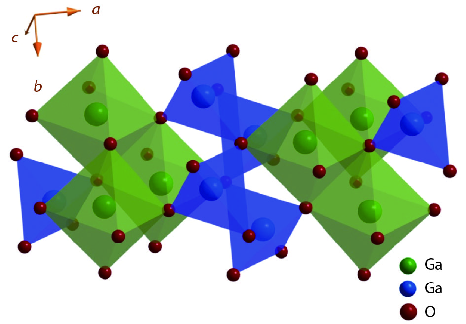
Fig. 1.
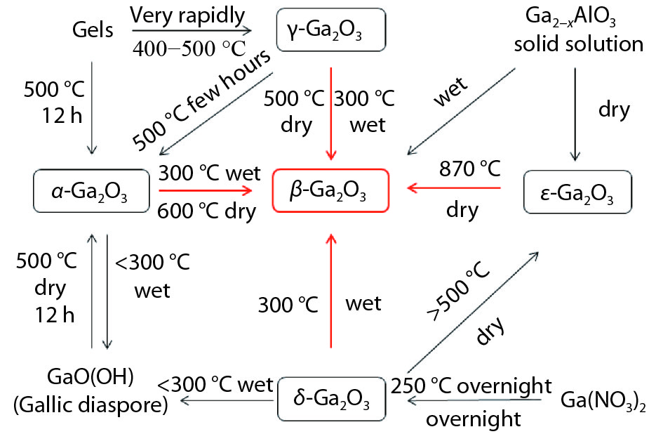
(Color online) Transformation relationships among Ga2O3 in different crystalline phases and their hydrates[21].
REVIEWS
Hang Dong1, 2, Huiwen Xue1, 2, Qiming He1, 2, Yuan Qin1, 2, Guangzhong Jian1, 2, Shibing Long1, 2, 3, and Ming Liu1, 2
Corresponding author: Shibing Long, E-mail: shibinglong@ustc.edu.cn
Abstract: As a promising ultra-wide bandgap semiconductor, gallium oxide (Ga2O3) has attracted increasing attention in recent years. The high theoretical breakdown electrical field (8 MV/cm), ultra-wide bandgap (~ 4.8 eV) and large Baliga’s figure of merit (BFOM) of Ga2O3 make it a potential candidate material for next generation high-power electronics, including diode and field effect transistor (FET). In this paper, we introduce the basic physical properties of Ga2O3 single crystal, and review the recent research process of Ga2O3 based field effect transistors. Furthermore, various structures of FETs have been summarized and compared, and the potential of Ga2O3 is preliminary revealed. Finally, the prospect of the Ga2O3 based FET for power electronics application is analyzed.
Keywords: gallium oxide (Ga2O3), ultra-wide bandgap semiconductor, power device, field effect transistor (FET)
| [1] |
J Millan, P Godignon, X Perpina, et al. A Survey of Wide Bandgap Power Semiconductor Devices. IEEE Trans Power Electron, 2014, 29(5): 2155 doi: 10.1109/TPEL.2013.2268900
|
| [2] |
Baliga B J. Fundamentals of power semiconductor devices. New York: Springer Science & Business Media, 2010
|
| [3] |
T P Chow, I Omura, M Higashiwaki, et al. Smart power devices and ICs using GaAs and wide and extreme bandgap semiconductors. IEEE Trans Electron Devices, 2017, 64(3): 856 doi: 10.1109/TED.2017.2653759
|
| [4] |
S Fujita. Wide-bandgap semiconductor materials: For their full bloom. Jpn J Appl Phys, 2015, 54(3): 030101 doi: 10.7567/JJAP.54.030101
|
| [5] |
M Higashiwaki, K Sasaki, A Kuramata, et al. Development of gallium oxide power device. Phys Status Solidi A, 2014, 211(1): 21 doi: 10.1002/pssa.201330197
|
| [6] |
M Higashiwaki, K Sasaki, H Murakami, et al. Recent progress in Ga2O3 power devices. Semicond Sci Technol, 2016, 31(3): 034001 doi: 10.1088/0268-1242/31/3/034001
|
| [7] |
N Ueda, H Hosono, R Waseda, et al. Synthesis and control of conductivity of ultraviolet transmitting β-Ga2O3 single crystals. Appl Phys Lett, 1997, 70(26): 3561 doi: 10.1063/1.119233
|
| [8] |
E G Víllora, K Shimamura, Y Yoshikawa, et al. Large-size β-Ga2O3 single crystals and wafers. J Cryst Growth, 2004, 270(3/4): 420
|
| [9] |
K N H Aida, H Takeda, N Aota, et al. Growth of β-Ga2O3 single crystals by the edge-defined, film fed growth method. Jpn J Appl Phys, 2008, 47(11): 8506 doi: 10.1143/JJAP.47.8506
|
| [10] |
M Higashiwaki, K Konishi, K Sasaki, et al. Temperature-dependent capacitance–voltage and current–voltage characteristics of Pt/Ga2O3 (001) Schottky barrier diodes fabricated on n-Ga2O3 drift layers grown by halide vapor phase epitaxy. Appl Phys Lett, 2016, 108(13): 133503 doi: 10.1063/1.4945267
|
| [11] |
M Higashiwaki, K Sasaki, T Kamimura, et al. Depletion-mode Ga2O3 metal–oxide–semiconductor field-effect transistors on β-Ga2O3 (010) substrates and temperature dependence of their device characteristics. Appl Phys Lett, 2013, 103(12): 123511 doi: 10.1063/1.4821858
|
| [12] |
M Higashiwaki, K Sasaki, A Kuramata, et al. Gallium oxide (Ga2O3) metal-semiconductor field-effect transistors on single-crystal β-Ga2O3 (010) substrates. Appl Phys Lett, 2012, 100(1): 013504 doi: 10.1063/1.3674287
|
| [13] |
W S Hwang, A Verma, H Peelaers, et al. High-voltage field effect transistors with wide-bandgap β-Ga2O3 nanomembranes. Appl Phys Lett, 2014, 104(20): 203111 doi: 10.1063/1.4879800
|
| [14] |
Z Hu, K Nomoto, W Li, et al. Enhancement-mode Ga2O3 vertical Transistors with breakdown voltage > 1 kV. IEEE Electron Device Lett, 2018, 39(6): 869 doi: 10.1109/LED.2018.2830184
|
| [15] |
K D Chabak, J P McCandless, N A Moser, et al. Recessed-gate enhancement-mode β-Ga2O3 MOSFETs. IEEE Electron Device Lett, 2018, 39(1): 67 doi: 10.1109/LED.2017.2779867
|
| [16] |
M. H. Wong, K. Sasaki, A. Kuramata, et al. Field-Plated Ga2O3 MOSFETs With a Breakdown Voltage of Over 750 V. IEEE Electron Device Lett, 2016, 37(2): 212-215 doi: 10.1109/LED.2015.2512279
|
| [17] |
H Zhou, M Si, S Alghamdi, et al. High performance depletion/enhancement-mode β-Ga2O3 on insulator (GOOI) field-effect transistors with record drain currents of 600/450 mA/mm. IEEE Electron Device Lett, 2017, 38(1): 103 doi: 10.1109/LED.2016.2635579
|
| [18] |
Q He, W Mu, B Fu, et al. Schottky barrier rectifier based on (100) β-Ga2O3 and its DC and AC characteristics. IEEE Electron Device Lett, 2018, 39(4): 556
|
| [19] |
K Sasaki, D Wakimoto, Q T Thieu, et al. First demonstration of Ga2O3 trench MOS-type Schottky barrier diodes. IEEE Electron Device Lett, 2017, 38(6): 783 doi: 10.1109/LED.2017.2696986
|
| [20] |
K Konishi, K Goto, H Murakami, et al. 1-kV vertical Ga2O3 field-plated Schottky barrier diodes. Appl Phys Lett, 2017, 110(10): 103506 doi: 10.1063/1.4977857
|
| [21] |
R Roy, Hill V G, Osborn E F. Polymorphism of Ga2O3 and the system Ga2O3–H2O. J Am Chem Soc, 1952, 74: 719 doi: 10.1021/ja01123a039
|
| [22] |
H H Tippins. Optical absorption and photoconductivity in the band edge of β-Ga2O3. Phys Rev, 1965, 140(1A): A316 doi: 10.1103/PhysRev.140.A316
|
| [23] |
T C Lovejoy, E N Yitamben, N. Shamir, et al. Surface morphology and electronic structure of bulk single crystal β-Ga2O3 (100). Appl Phys Lett, 2009, 94(8): 081906 doi: 10.1063/1.3086392
|
| [24] |
M Mohamed, C Janowitz, I Unger, et al. The electronic structure of β-Ga2O3. Appl Phys Lett, 2010, 97(21): 211903 doi: 10.1063/1.3521255
|
| [25] |
C Janowitz, V Scherer, M Mohamed, et al. Experimental electronic structure of In2O3 and Ga2O3. New J Phys, 2011, 13(8): 085014 doi: 10.1088/1367-2630/13/8/085014
|
| [26] |
O Ueda, N Ikenag, K Koshi, et al. Structural evaluation of defects in β-Ga2O3 single crystals grown by edge-defined film-fed growth process. Jpn J Appl Phys, 2016, 55(12): 1202BD
|
| [27] |
F Mezzadri, G Calestani, F Boschi, et al. Crystal structure and ferroelectric properties of epsilon-Ga2O3 films grown on (0001)-sapphire. Inorg Chem, 2016, 55(22): 2079
|
| [28] |
X Xia, Y Chen, Q Feng, et al. Hexagonal phase-pure wide band gap ε-Ga2O3 films grown on 6H-SiC substrates by metal organic chemical vapor deposition. Appl Phys Lett, 2016, 108(20): 202103 doi: 10.1063/1.4950867
|
| [29] |
M Slomski, N Blumenschein, P P Paskov, et al. Anisotropic thermal conductivity of β-Ga2O3 at elevated temperatures: Effect of Sn and Fe dopants. J Appl Phys, 2017, 121(23): 235104 doi: 10.1063/1.4986478
|
| [30] |
K Hoshikawa, E Oh, T Kobayashi, et al. Growth of β-Ga2O3 single crystals using vertical Bridgman method in ambient air. J Cryst Growth, 2016, 447: 36 doi: 10.1016/j.jcrysgro.2016.04.022
|
| [31] |
S Yoshioka, H Hayashi, A Kuwabara, et al. Structures and energetics of Ga2O3 polymorphs. J Phys-Condens Mat, 2007, 19(34): 346211 doi: 10.1088/0953-8984/19/34/346211
|
| [32] |
J Åhman, G Svensson, J Albertsson. A reinvestigation of beta-gallium oxide. Acta Crystallogr C, 1996, 52(6): 1336 doi: 10.1107/S0108270195016404
|
| [33] |
A Janotti, C G Van de Walle. Oxygen vacancies in ZnO. Appl Phys Lett, 2005, 87(12): 122102 doi: 10.1063/1.2053360
|
| [34] |
T Oshima, K Kaminaga, A Mukai, et al. Formation of semi-insulating layers on semiconducting β-Ga2O3 single crystals by thermal oxidation. Jpn J Appl Phys, 2013, 52(5R): 051101 doi: 10.7567/JJAP.52.051101
|
| [35] |
J B Varley, J R Weber, A Janotti, et al. Oxygen vacancies and donor impurities in β-Ga2O3. Appl Phys Lett, 2010, 97(14): 142106 doi: 10.1063/1.3499306
|
| [36] |
Z Hajnal, J Miró, G Kiss, et al. Role of oxygen vacancy defect states in then-type conduction of β-Ga2O3. J Appl Phys, 1999, 86(7): 3792 doi: 10.1063/1.371289
|
| [37] |
J G M Fleischer, H Meixner. H2-induced changes in electrical conductance of β-Ga2O3 thin-film systems. Appl Phys A, 1992, 54: 560 doi: 10.1007/BF00324340
|
| [38] |
F B C K A F M F C Kohl. Decomposition of methane on polycrystalline thick films of Ga2O3 investigated by thermal desorption spectroscopy with a mass spectrometer. Fresenius J Ana Chem, 1997, 358: 187 doi: 10.1007/s002160050379
|
| [39] |
M F T Schwebel, H Meixner, C D Kohl. CO-sensor for domestic use based on high temperature stable Ga2O3 thin films. Sens Actuators B Chem, 1998, 49: 46 doi: 10.1016/S0925-4005(97)00334-1
|
| [40] |
K H M Ogita, Y Nakanishi, Y Hatanaka. Ga2O3 thin film for oxygen sensor at high temperature. Appl Surf Sci, 2001, 175: 721
|
| [41] |
Z Guo, A Verma, X Wu, et al. Anisotropic thermal conductivity in single crystal β-gallium oxide. Appl Phys Lett, 2015, 106(11): 111909 doi: 10.1063/1.4916078
|
| [42] |
M Handwerg, R Mitdank, Z Galazka, et al. Temperature-dependent thermal conductivity in Mg-doped and undoped β-Ga2O3 bulk-crystals. Semicond Sci Tech, 2015, 30(2): 024006 doi: 10.1088/0268-1242/30/2/024006
|
| [43] |
M D Santia, N Tandon, J D Albrecht. Lattice thermal conductivity in β-Ga2O3 from first principles. Appl Phys Lett, 2015, 107(4): 041907 doi: 10.1063/1.4927742
|
| [44] |
Wang H. Investigation of power semiconductor devices for high frequency high density power converters. Virgina Tech, 2007
|
| [45] |
Jessen G, Chabak K D, Green A, et al. Toward realization of Ga2O3 for power electronics applications. The 75th IEEE Device Research Conference (DRC), 2017
|
| [46] |
N Ma, N Tanen, A Verma, et al. Intrinsic electron mobility limits in β-Ga2O3. Appl Phys Lett, 2016, 109(21): 212101 doi: 10.1063/1.4968550
|
| [47] |
T Oishi, Y Koga, K Harada, et al. High-mobility β-Ga2O3 (-201) single crystals grown by edge-defined film-fed growth method and their Schottky barrier diodes with Ni contact. Appl Phys Express, 2015, 8(3): 031101 doi: 10.7567/APEX.8.031101
|
| [48] |
M Higashiwaki, A Kuramata, H Murakami, et al. State-of-the-art technologies of gallium oxide power devices. J Phys D Appl Phys, 2017, 50(33): 333002 doi: 10.1088/1361-6463/aa7aff
|
| [49] |
C Tang, J Sun, N Lin, et al. Electronic structure and optical property of metal-doped Ga2O3: a first principles study. RSC Adv, 2016, 6(82): 78322 doi: 10.1039/C6RA14010F
|
| [50] |
H Peelaers, C G Van de Walle. Brillouin zone and band structure of β-Ga2O3. Phys Status Solidi B, 2015, 252(4): 828 doi: 10.1002/pssb.201451551
|
| [51] |
H von Wenckstern. Group-III sesquioxides: growth, physical properties and devices. Adv Electron Mater, 2017, 3(9): 1600350 doi: 10.1002/aelm.v3.9
|
| [52] |
K Sasaki, M Higashiwaki, A Kuramata, et al. MBE grown Ga2O3 and its power device applications. J Crys Growth, 2013, 378: 591 doi: 10.1016/j.jcrysgro.2013.02.015
|
| [53] |
M H Wong, Y Morikawa, K Sasaki, et al. Characterization of channel temperature in Ga2O3 metal–oxide–semiconductor field-effect transistors by electrical measurements and thermal modeling. Appl Phys Lett, 2016, 109(19): 193503 doi: 10.1063/1.4966999
|
| [54] |
Wong M H, Takeyama A, Makino T, et al. Radiation hardness of Ga2O3 MOSFETs against gamma-ray irradiation. IEEE Device Research Conference (DRC), 2017
|
| [55] |
A J Green, K D Chabak, E R Heller, et al. 3.8-MV/cm breakdown strength of MOVPE-grown Sn-doped β-Ga2O3 MOSFETs. IEEE Electron Device Lett, 2016, 37(7): 902 doi: 10.1109/LED.2016.2568139
|
| [56] |
M H Wong, Y Nakata, A Kuramata, et al. Enhancement-mode Ga2O3 MOSFETs with Si-ion-implanted source and drain. Appl Phys Express, 2017, 10: 041101 doi: 10.7567/APEX.10.041101
|
| [57] |
Wong M, Goto K, Kuramata A, et al. First demonstration of vertical Ga2O3 MOSFET planar structure with a current aperture. IEEE Device Research Conference (DRC), 2017
|
| [58] |
Song B, Verma A K, Nomoto K, et al. Vertical Fin Ga2O3 power field-effect transistors with on/off ratio >109. IEEE Device Research Conference (DRC), 2017
|
| [59] |
A J Green, K D Chabak, M Baldini, et al. β-Ga2O3 MOSFETs for radio frequency operation. IEEE Electron Device Lett, 2017, 38(6): 790 doi: 10.1109/LED.2017.2694805
|
| [60] |
S Krishnamoorthy, Z Xia, S Bajaj, et al. Delta-doped β-gallium oxide field-effect transistor. Appl Phys Express, 2017, 10(5): 051102 doi: 10.7567/APEX.10.051102
|
| [61] |
Z Xia, C Joishi, S Krishnamoorthy, et al. Delta doped β-Ga2O3 field effect transistors with regrown ohmic contacts. IEEE Electron Device Lett, 2018, 39(4): 568 doi: 10.1109/LED.2018.2805785
|
| [62] |
Hwang A V W S, Protasenko V, Rouvimov S, et al. Nanomembrane β-Ga2O3 high-voltage field effect transistors. IEEE Device Research Conference (DRC), 2013
|
| [63] |
S Ahn, F Ren, J Kim, et al. Effect of front and back gates on β-Ga2O3 nano-belt field-effect transistors. Appl Phys Lett, 2016, 109(6): 062102 doi: 10.1063/1.4960651
|
| [64] |
J Bae, H W Kim, I H Kang, et al. High breakdown voltage quasi-two-dimensional β-Ga2O3 field-effect transistors with a boron nitride field plate. Appl Phys Lett, 2018, 112(12): 122102 doi: 10.1063/1.5018238
|
| [65] |
H Zhou, K Maize, G Qiu, et al. β-Ga2O3 on insulator field-effect transistors with drain currents exceeding 1.5 A/mm and their self-heating effect. Appl Phys Lett, 2017, 111(9): 092102 doi: 10.1063/1.5000735
|
| [66] |
H Zhou, S Alghamdi, S W Si, et al. Al2O3/β-Ga2O3 (-201) interface improvement through piranha pretreatment and postdeposition annealing. IEEE Electron Device Lett, 2016, 37(11): 1411 doi: 10.1109/LED.2016.2609202
|
| [67] |
T Kamimura, D Krishnamurthy, A Kuramata, et al. Epitaxially grown crystalline Al2O3 interlayer on β-Ga2O3 (010) and its suppressed interface state density. Jpn J Appl Phys, 2016, 55(12): 1202B5
|
| [68] |
M Hattori, T Oshima, R Wakabayashi, et al. Epitaxial growth and electric properties of γ-Al2O3 (110) films on β-Ga2O3 (010) substrates. Jpn J Appl Phys, 2016, 55(12): 1202B6
|
| [69] |
K Zeng, Y Jia, U Singisetti. Interface state density in atomic layer deposited SiO2/β-Ga2O3 MOSCAPs. IEEE Electron Device Lett, 2016, 37(7): 906 doi: 10.1109/LED.2016.2570521
|
| [70] |
K Zeng, U Singisetti. Temperature dependent quasi-static capacitance-voltage characterization of SiO2/β-Ga2O3 interface on different crystal orientations. Appl Phys Lett, 2017, 111(12): 122108 doi: 10.1063/1.4991400
|
| [71] |
H Dong, W Mu, Y Hu, et al. C-V and J-V investigation of HfO2/Al2O3 bilayer dielectrics MOSCAPs on (100) β-Ga2O3. AIP Adv, 2018, 8(6): 065215 doi: 10.1063/1.5031183
|
| [72] |
M A Bhuiyan, H Zhou, R Jiang, et al. Charge trapping in Al2O3/β-Ga2O3 based MOS capacitors. IEEE Electron Device Lett, 2018, 39(7): 1022 doi: 10.1109/LED.2018.2841899
|
| [73] |
Y Yao, R F Davis, L M Porter. Investigation of different metals as ohmic contacts to β-Ga2O3: comparison and analysis of electrical behavior, morphology, and other physical properties. J Electron Mater, 2016, 46(4): 2053
|
| [74] |
N A Moser, J P McCandless, A Crespo, et al. High pulsed current density β-Ga2O3 MOSFETs verified by an analytical model corrected for interface charge. Appl Phys Lett, 2017, 110(14): 143505 doi: 10.1063/1.4979789
|
| [75] |
K Sasaki, Q T Thieu, D Wakimoto, et al. Depletion-mode vertical Ga2O3 trench MOSFETs fabricated using Ga2O3 homoepitaxial films grown by halide vapor phase epitaxy. Appl Phys Express, 2017, 10(12): 124201. doi: 10.7567/APEX.10.124201
|
| [76] |
K Zeng, J S Wallace, C Heimburger, et al. Ga2O3 MOSFETs using spin-on-glass source/drain doping technology. IEEE Electron Device Lett, 2017, 38(4): 513-516 doi: 10.1109/LED.2017.2675544
|
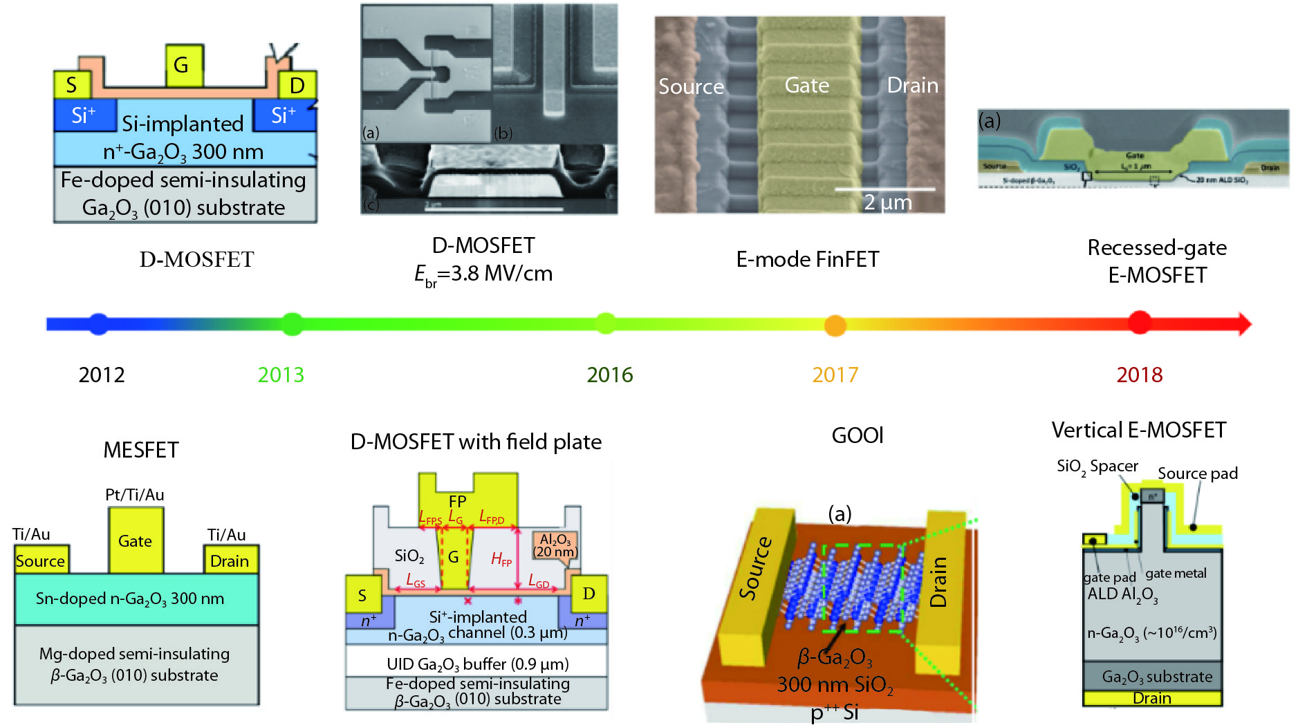
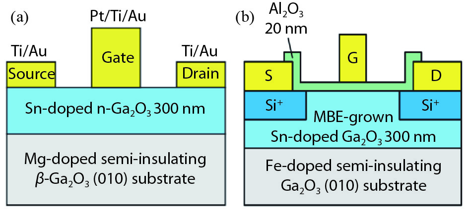
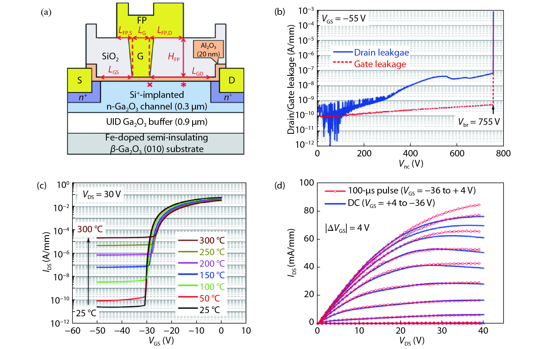
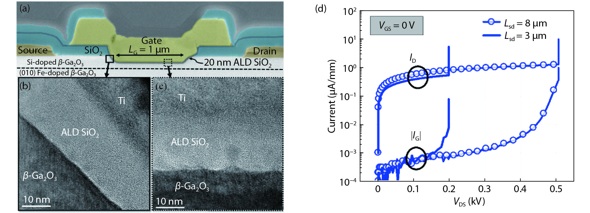
Table 1. Comparison of the physical properties of Si, GaN, SiC and β-Ga2O3 semiconductor[6].
| Semiconductor material | Si | GaN | 4H-SiC | β-Ga2O3 |
| Bandgap Eg (eV) | 1.1 | 3.4 | 3.3 | 4.7–4.9 |
| Electron mobility μ (cm2·V−1·s−1) | 1400 | 1200 | 1000 | 300 |
| Breakdown electric field Eb (MV/cm) | 0.3 | 3.3 | 2.5 | 8 |
| Baliga’s FOM (εμEb3) | 1 | 870 | 340 | 3444 |
| Thermal conductivity λ (W·cm−1·K−1) | 1.5 | 2.1 | 2.7 | 0.11 |
 DownLoad: CSV
Table 2. Development of Ga2O3 FETs and the corresponding performances.
| Device type | Substrateorientation | Gate dielectrics | Vbr (V) | Jmax (mA/mm) | On/off ratio | gm (mS/mm) | Reference |
| D-MESFET | (010) β-Ga2O3 | — | 250 | — | 104 | 1.4 | [12] |
| D-MOSFET | (010) β-Ga2O3 | Al2O3 | 370 | 39 | 1010 | — | [11] |
| E-Fin FET | (100) β-Ga2O3 | Al2O3 | 600 | - | 105 | — | [15] |
| Two-finger D-MOSFET | (100) β-Ga2O3 | Al2O3 | 230 | 60 | 107 | 1.1 | [55] |
| Field plate D-MOSFET | (010) β-Ga2O3 | Al2O3 | 750 | 78 | 109 | 3.4 | [16] |
| Recessed-gate D-MOSFET | (100) β-Ga2O3 | Al2O3 | — | 150 | 106 | 21.2 | [59] |
| E-MOSFET | (010) β-Ga2O3 | Al2O3 | — | 1.4 | 106 | 0.38 | [56] |
| D-MOSFET | (010) β-Ga2O3 | HfO2 | 400 | 45 | 108 | — | [74] |
| Vertical trench D-MOSFET | (001) β-Ga2O3 | HfO2 | — | — | 103 | — | [75] |
| Vertical Fin D-MOSFET | (-201) β-Ga2O3 | Al2O3 | 185 | 1 kA/cm2 | 109 | — | [58] |
| D-MOSFET | β-Ga2O3 | SiO2 | 382 | 40 | 108 | 1.23 | [76] |
| Recessed-gate E-MOSFET | (010) β-Ga2O3 | SiO2 | 505 | 40 | 109 | 7 | [15] |
| Vertical Fin E-MISFET | (001) β-Ga2O3 | Al2O3 | 1057 | 300–500 kA/cm2 | 108 | — | [14] |
| Delta doped D-MOSFET | (010) β-Ga2O3 | — | 170 | 140 | 106 | 34 | [61] |
DownLoad: CSV
| [1] |
J Millan, P Godignon, X Perpina, et al. A Survey of Wide Bandgap Power Semiconductor Devices. IEEE Trans Power Electron, 2014, 29(5): 2155 doi: 10.1109/TPEL.2013.2268900
|
| [2] |
Baliga B J. Fundamentals of power semiconductor devices. New York: Springer Science & Business Media, 2010
|
| [3] |
T P Chow, I Omura, M Higashiwaki, et al. Smart power devices and ICs using GaAs and wide and extreme bandgap semiconductors. IEEE Trans Electron Devices, 2017, 64(3): 856 doi: 10.1109/TED.2017.2653759
|
| [4] |
S Fujita. Wide-bandgap semiconductor materials: For their full bloom. Jpn J Appl Phys, 2015, 54(3): 030101 doi: 10.7567/JJAP.54.030101
|
| [5] |
M Higashiwaki, K Sasaki, A Kuramata, et al. Development of gallium oxide power device. Phys Status Solidi A, 2014, 211(1): 21 doi: 10.1002/pssa.201330197
|
| [6] |
M Higashiwaki, K Sasaki, H Murakami, et al. Recent progress in Ga2O3 power devices. Semicond Sci Technol, 2016, 31(3): 034001 doi: 10.1088/0268-1242/31/3/034001
|
| [7] |
N Ueda, H Hosono, R Waseda, et al. Synthesis and control of conductivity of ultraviolet transmitting β-Ga2O3 single crystals. Appl Phys Lett, 1997, 70(26): 3561 doi: 10.1063/1.119233
|
| [8] |
E G Víllora, K Shimamura, Y Yoshikawa, et al. Large-size β-Ga2O3 single crystals and wafers. J Cryst Growth, 2004, 270(3/4): 420
|
| [9] |
K N H Aida, H Takeda, N Aota, et al. Growth of β-Ga2O3 single crystals by the edge-defined, film fed growth method. Jpn J Appl Phys, 2008, 47(11): 8506 doi: 10.1143/JJAP.47.8506
|
| [10] |
M Higashiwaki, K Konishi, K Sasaki, et al. Temperature-dependent capacitance–voltage and current–voltage characteristics of Pt/Ga2O3 (001) Schottky barrier diodes fabricated on n-Ga2O3 drift layers grown by halide vapor phase epitaxy. Appl Phys Lett, 2016, 108(13): 133503 doi: 10.1063/1.4945267
|
| [11] |
M Higashiwaki, K Sasaki, T Kamimura, et al. Depletion-mode Ga2O3 metal–oxide–semiconductor field-effect transistors on β-Ga2O3 (010) substrates and temperature dependence of their device characteristics. Appl Phys Lett, 2013, 103(12): 123511 doi: 10.1063/1.4821858
|
| [12] |
M Higashiwaki, K Sasaki, A Kuramata, et al. Gallium oxide (Ga2O3) metal-semiconductor field-effect transistors on single-crystal β-Ga2O3 (010) substrates. Appl Phys Lett, 2012, 100(1): 013504 doi: 10.1063/1.3674287
|
| [13] |
W S Hwang, A Verma, H Peelaers, et al. High-voltage field effect transistors with wide-bandgap β-Ga2O3 nanomembranes. Appl Phys Lett, 2014, 104(20): 203111 doi: 10.1063/1.4879800
|
| [14] |
Z Hu, K Nomoto, W Li, et al. Enhancement-mode Ga2O3 vertical Transistors with breakdown voltage > 1 kV. IEEE Electron Device Lett, 2018, 39(6): 869 doi: 10.1109/LED.2018.2830184
|
| [15] |
K D Chabak, J P McCandless, N A Moser, et al. Recessed-gate enhancement-mode β-Ga2O3 MOSFETs. IEEE Electron Device Lett, 2018, 39(1): 67 doi: 10.1109/LED.2017.2779867
|
| [16] |
M. H. Wong, K. Sasaki, A. Kuramata, et al. Field-Plated Ga2O3 MOSFETs With a Breakdown Voltage of Over 750 V. IEEE Electron Device Lett, 2016, 37(2): 212-215 doi: 10.1109/LED.2015.2512279
|
| [17] |
H Zhou, M Si, S Alghamdi, et al. High performance depletion/enhancement-mode β-Ga2O3 on insulator (GOOI) field-effect transistors with record drain currents of 600/450 mA/mm. IEEE Electron Device Lett, 2017, 38(1): 103 doi: 10.1109/LED.2016.2635579
|
| [18] |
Q He, W Mu, B Fu, et al. Schottky barrier rectifier based on (100) β-Ga2O3 and its DC and AC characteristics. IEEE Electron Device Lett, 2018, 39(4): 556
|
| [19] |
K Sasaki, D Wakimoto, Q T Thieu, et al. First demonstration of Ga2O3 trench MOS-type Schottky barrier diodes. IEEE Electron Device Lett, 2017, 38(6): 783 doi: 10.1109/LED.2017.2696986
|
| [20] |
K Konishi, K Goto, H Murakami, et al. 1-kV vertical Ga2O3 field-plated Schottky barrier diodes. Appl Phys Lett, 2017, 110(10): 103506 doi: 10.1063/1.4977857
|
| [21] |
R Roy, Hill V G, Osborn E F. Polymorphism of Ga2O3 and the system Ga2O3–H2O. J Am Chem Soc, 1952, 74: 719 doi: 10.1021/ja01123a039
|
| [22] |
H H Tippins. Optical absorption and photoconductivity in the band edge of β-Ga2O3. Phys Rev, 1965, 140(1A): A316 doi: 10.1103/PhysRev.140.A316
|
| [23] |
T C Lovejoy, E N Yitamben, N. Shamir, et al. Surface morphology and electronic structure of bulk single crystal β-Ga2O3 (100). Appl Phys Lett, 2009, 94(8): 081906 doi: 10.1063/1.3086392
|
| [24] |
M Mohamed, C Janowitz, I Unger, et al. The electronic structure of β-Ga2O3. Appl Phys Lett, 2010, 97(21): 211903 doi: 10.1063/1.3521255
|
| [25] |
C Janowitz, V Scherer, M Mohamed, et al. Experimental electronic structure of In2O3 and Ga2O3. New J Phys, 2011, 13(8): 085014 doi: 10.1088/1367-2630/13/8/085014
|
| [26] |
O Ueda, N Ikenag, K Koshi, et al. Structural evaluation of defects in β-Ga2O3 single crystals grown by edge-defined film-fed growth process. Jpn J Appl Phys, 2016, 55(12): 1202BD
|
| [27] |
F Mezzadri, G Calestani, F Boschi, et al. Crystal structure and ferroelectric properties of epsilon-Ga2O3 films grown on (0001)-sapphire. Inorg Chem, 2016, 55(22): 2079
|
| [28] |
X Xia, Y Chen, Q Feng, et al. Hexagonal phase-pure wide band gap ε-Ga2O3 films grown on 6H-SiC substrates by metal organic chemical vapor deposition. Appl Phys Lett, 2016, 108(20): 202103 doi: 10.1063/1.4950867
|
| [29] |
M Slomski, N Blumenschein, P P Paskov, et al. Anisotropic thermal conductivity of β-Ga2O3 at elevated temperatures: Effect of Sn and Fe dopants. J Appl Phys, 2017, 121(23): 235104 doi: 10.1063/1.4986478
|
| [30] |
K Hoshikawa, E Oh, T Kobayashi, et al. Growth of β-Ga2O3 single crystals using vertical Bridgman method in ambient air. J Cryst Growth, 2016, 447: 36 doi: 10.1016/j.jcrysgro.2016.04.022
|
| [31] |
S Yoshioka, H Hayashi, A Kuwabara, et al. Structures and energetics of Ga2O3 polymorphs. J Phys-Condens Mat, 2007, 19(34): 346211 doi: 10.1088/0953-8984/19/34/346211
|
| [32] |
J Åhman, G Svensson, J Albertsson. A reinvestigation of beta-gallium oxide. Acta Crystallogr C, 1996, 52(6): 1336 doi: 10.1107/S0108270195016404
|
| [33] |
A Janotti, C G Van de Walle. Oxygen vacancies in ZnO. Appl Phys Lett, 2005, 87(12): 122102 doi: 10.1063/1.2053360
|
| [34] |
T Oshima, K Kaminaga, A Mukai, et al. Formation of semi-insulating layers on semiconducting β-Ga2O3 single crystals by thermal oxidation. Jpn J Appl Phys, 2013, 52(5R): 051101 doi: 10.7567/JJAP.52.051101
|
| [35] |
J B Varley, J R Weber, A Janotti, et al. Oxygen vacancies and donor impurities in β-Ga2O3. Appl Phys Lett, 2010, 97(14): 142106 doi: 10.1063/1.3499306
|
| [36] |
Z Hajnal, J Miró, G Kiss, et al. Role of oxygen vacancy defect states in then-type conduction of β-Ga2O3. J Appl Phys, 1999, 86(7): 3792 doi: 10.1063/1.371289
|
| [37] |
J G M Fleischer, H Meixner. H2-induced changes in electrical conductance of β-Ga2O3 thin-film systems. Appl Phys A, 1992, 54: 560 doi: 10.1007/BF00324340
|
| [38] |
F B C K A F M F C Kohl. Decomposition of methane on polycrystalline thick films of Ga2O3 investigated by thermal desorption spectroscopy with a mass spectrometer. Fresenius J Ana Chem, 1997, 358: 187 doi: 10.1007/s002160050379
|
| [39] |
M F T Schwebel, H Meixner, C D Kohl. CO-sensor for domestic use based on high temperature stable Ga2O3 thin films. Sens Actuators B Chem, 1998, 49: 46 doi: 10.1016/S0925-4005(97)00334-1
|
| [40] |
K H M Ogita, Y Nakanishi, Y Hatanaka. Ga2O3 thin film for oxygen sensor at high temperature. Appl Surf Sci, 2001, 175: 721
|
| [41] |
Z Guo, A Verma, X Wu, et al. Anisotropic thermal conductivity in single crystal β-gallium oxide. Appl Phys Lett, 2015, 106(11): 111909 doi: 10.1063/1.4916078
|
| [42] |
M Handwerg, R Mitdank, Z Galazka, et al. Temperature-dependent thermal conductivity in Mg-doped and undoped β-Ga2O3 bulk-crystals. Semicond Sci Tech, 2015, 30(2): 024006 doi: 10.1088/0268-1242/30/2/024006
|
| [43] |
M D Santia, N Tandon, J D Albrecht. Lattice thermal conductivity in β-Ga2O3 from first principles. Appl Phys Lett, 2015, 107(4): 041907 doi: 10.1063/1.4927742
|
| [44] |
Wang H. Investigation of power semiconductor devices for high frequency high density power converters. Virgina Tech, 2007
|
| [45] |
Jessen G, Chabak K D, Green A, et al. Toward realization of Ga2O3 for power electronics applications. The 75th IEEE Device Research Conference (DRC), 2017
|
| [46] |
N Ma, N Tanen, A Verma, et al. Intrinsic electron mobility limits in β-Ga2O3. Appl Phys Lett, 2016, 109(21): 212101 doi: 10.1063/1.4968550
|
| [47] |
T Oishi, Y Koga, K Harada, et al. High-mobility β-Ga2O3 (-201) single crystals grown by edge-defined film-fed growth method and their Schottky barrier diodes with Ni contact. Appl Phys Express, 2015, 8(3): 031101 doi: 10.7567/APEX.8.031101
|
| [48] |
M Higashiwaki, A Kuramata, H Murakami, et al. State-of-the-art technologies of gallium oxide power devices. J Phys D Appl Phys, 2017, 50(33): 333002 doi: 10.1088/1361-6463/aa7aff
|
| [49] |
C Tang, J Sun, N Lin, et al. Electronic structure and optical property of metal-doped Ga2O3: a first principles study. RSC Adv, 2016, 6(82): 78322 doi: 10.1039/C6RA14010F
|
| [50] |
H Peelaers, C G Van de Walle. Brillouin zone and band structure of β-Ga2O3. Phys Status Solidi B, 2015, 252(4): 828 doi: 10.1002/pssb.201451551
|
| [51] |
H von Wenckstern. Group-III sesquioxides: growth, physical properties and devices. Adv Electron Mater, 2017, 3(9): 1600350 doi: 10.1002/aelm.v3.9
|
| [52] |
K Sasaki, M Higashiwaki, A Kuramata, et al. MBE grown Ga2O3 and its power device applications. J Crys Growth, 2013, 378: 591 doi: 10.1016/j.jcrysgro.2013.02.015
|
| [53] |
M H Wong, Y Morikawa, K Sasaki, et al. Characterization of channel temperature in Ga2O3 metal–oxide–semiconductor field-effect transistors by electrical measurements and thermal modeling. Appl Phys Lett, 2016, 109(19): 193503 doi: 10.1063/1.4966999
|
| [54] |
Wong M H, Takeyama A, Makino T, et al. Radiation hardness of Ga2O3 MOSFETs against gamma-ray irradiation. IEEE Device Research Conference (DRC), 2017
|
| [55] |
A J Green, K D Chabak, E R Heller, et al. 3.8-MV/cm breakdown strength of MOVPE-grown Sn-doped β-Ga2O3 MOSFETs. IEEE Electron Device Lett, 2016, 37(7): 902 doi: 10.1109/LED.2016.2568139
|
| [56] |
M H Wong, Y Nakata, A Kuramata, et al. Enhancement-mode Ga2O3 MOSFETs with Si-ion-implanted source and drain. Appl Phys Express, 2017, 10: 041101 doi: 10.7567/APEX.10.041101
|
| [57] |
Wong M, Goto K, Kuramata A, et al. First demonstration of vertical Ga2O3 MOSFET planar structure with a current aperture. IEEE Device Research Conference (DRC), 2017
|
| [58] |
Song B, Verma A K, Nomoto K, et al. Vertical Fin Ga2O3 power field-effect transistors with on/off ratio >109. IEEE Device Research Conference (DRC), 2017
|
| [59] |
A J Green, K D Chabak, M Baldini, et al. β-Ga2O3 MOSFETs for radio frequency operation. IEEE Electron Device Lett, 2017, 38(6): 790 doi: 10.1109/LED.2017.2694805
|
| [60] |
S Krishnamoorthy, Z Xia, S Bajaj, et al. Delta-doped β-gallium oxide field-effect transistor. Appl Phys Express, 2017, 10(5): 051102 doi: 10.7567/APEX.10.051102
|
| [61] |
Z Xia, C Joishi, S Krishnamoorthy, et al. Delta doped β-Ga2O3 field effect transistors with regrown ohmic contacts. IEEE Electron Device Lett, 2018, 39(4): 568 doi: 10.1109/LED.2018.2805785
|
| [62] |
Hwang A V W S, Protasenko V, Rouvimov S, et al. Nanomembrane β-Ga2O3 high-voltage field effect transistors. IEEE Device Research Conference (DRC), 2013
|
| [63] |
S Ahn, F Ren, J Kim, et al. Effect of front and back gates on β-Ga2O3 nano-belt field-effect transistors. Appl Phys Lett, 2016, 109(6): 062102 doi: 10.1063/1.4960651
|
| [64] |
J Bae, H W Kim, I H Kang, et al. High breakdown voltage quasi-two-dimensional β-Ga2O3 field-effect transistors with a boron nitride field plate. Appl Phys Lett, 2018, 112(12): 122102 doi: 10.1063/1.5018238
|
| [65] |
H Zhou, K Maize, G Qiu, et al. β-Ga2O3 on insulator field-effect transistors with drain currents exceeding 1.5 A/mm and their self-heating effect. Appl Phys Lett, 2017, 111(9): 092102 doi: 10.1063/1.5000735
|
| [66] |
H Zhou, S Alghamdi, S W Si, et al. Al2O3/β-Ga2O3 (-201) interface improvement through piranha pretreatment and postdeposition annealing. IEEE Electron Device Lett, 2016, 37(11): 1411 doi: 10.1109/LED.2016.2609202
|
| [67] |
T Kamimura, D Krishnamurthy, A Kuramata, et al. Epitaxially grown crystalline Al2O3 interlayer on β-Ga2O3 (010) and its suppressed interface state density. Jpn J Appl Phys, 2016, 55(12): 1202B5
|
| [68] |
M Hattori, T Oshima, R Wakabayashi, et al. Epitaxial growth and electric properties of γ-Al2O3 (110) films on β-Ga2O3 (010) substrates. Jpn J Appl Phys, 2016, 55(12): 1202B6
|
| [69] |
K Zeng, Y Jia, U Singisetti. Interface state density in atomic layer deposited SiO2/β-Ga2O3 MOSCAPs. IEEE Electron Device Lett, 2016, 37(7): 906 doi: 10.1109/LED.2016.2570521
|
| [70] |
K Zeng, U Singisetti. Temperature dependent quasi-static capacitance-voltage characterization of SiO2/β-Ga2O3 interface on different crystal orientations. Appl Phys Lett, 2017, 111(12): 122108 doi: 10.1063/1.4991400
|
| [71] |
H Dong, W Mu, Y Hu, et al. C-V and J-V investigation of HfO2/Al2O3 bilayer dielectrics MOSCAPs on (100) β-Ga2O3. AIP Adv, 2018, 8(6): 065215 doi: 10.1063/1.5031183
|
| [72] |
M A Bhuiyan, H Zhou, R Jiang, et al. Charge trapping in Al2O3/β-Ga2O3 based MOS capacitors. IEEE Electron Device Lett, 2018, 39(7): 1022 doi: 10.1109/LED.2018.2841899
|
| [73] |
Y Yao, R F Davis, L M Porter. Investigation of different metals as ohmic contacts to β-Ga2O3: comparison and analysis of electrical behavior, morphology, and other physical properties. J Electron Mater, 2016, 46(4): 2053
|
| [74] |
N A Moser, J P McCandless, A Crespo, et al. High pulsed current density β-Ga2O3 MOSFETs verified by an analytical model corrected for interface charge. Appl Phys Lett, 2017, 110(14): 143505 doi: 10.1063/1.4979789
|
| [75] |
K Sasaki, Q T Thieu, D Wakimoto, et al. Depletion-mode vertical Ga2O3 trench MOSFETs fabricated using Ga2O3 homoepitaxial films grown by halide vapor phase epitaxy. Appl Phys Express, 2017, 10(12): 124201. doi: 10.7567/APEX.10.124201
|
| [76] |
K Zeng, J S Wallace, C Heimburger, et al. Ga2O3 MOSFETs using spin-on-glass source/drain doping technology. IEEE Electron Device Lett, 2017, 38(4): 513-516 doi: 10.1109/LED.2017.2675544
|


Article views: 9032 Times PDF downloads: 745 Times Cited by: 0 Times
Received: 05 August 2018 Revised: 20 September 2018 Online: Accepted Manuscript: 20 December 2018Uncorrected proof: 25 December 2018Published: 07 January 2019
| Citation: |
Hang Dong, Huiwen Xue, Qiming He, Yuan Qin, Guangzhong Jian, Shibing Long, Ming Liu. Progress of power field effect transistor based on ultra-wide bandgap Ga2O3 semiconductor material[J]. Journal of Semiconductors, 2019, 40(1): 011802. doi: 10.1088/1674-4926/40/1/011802
****
H Dong, H W Xue, Q M He, Y Qin, G Z Jian, S B Long, M Liu, Progress of power field effect transistor based on ultra-wide bandgap Ga2O3 semiconductor material[J]. J. Semicond., 2019, 40(1): 011802. doi: 10.1088/1674-4926/40/1/011802.

|
| [1] |
J Millan, P Godignon, X Perpina, et al. A Survey of Wide Bandgap Power Semiconductor Devices. IEEE Trans Power Electron, 2014, 29(5): 2155 doi: 10.1109/TPEL.2013.2268900
|
| [2] |
Baliga B J. Fundamentals of power semiconductor devices. New York: Springer Science & Business Media, 2010
|
| [3] |
T P Chow, I Omura, M Higashiwaki, et al. Smart power devices and ICs using GaAs and wide and extreme bandgap semiconductors. IEEE Trans Electron Devices, 2017, 64(3): 856 doi: 10.1109/TED.2017.2653759
|
| [4] |
S Fujita. Wide-bandgap semiconductor materials: For their full bloom. Jpn J Appl Phys, 2015, 54(3): 030101 doi: 10.7567/JJAP.54.030101
|
| [5] |
M Higashiwaki, K Sasaki, A Kuramata, et al. Development of gallium oxide power device. Phys Status Solidi A, 2014, 211(1): 21 doi: 10.1002/pssa.201330197
|
| [6] |
M Higashiwaki, K Sasaki, H Murakami, et al. Recent progress in Ga2O3 power devices. Semicond Sci Technol, 2016, 31(3): 034001 doi: 10.1088/0268-1242/31/3/034001
|
| [7] |
N Ueda, H Hosono, R Waseda, et al. Synthesis and control of conductivity of ultraviolet transmitting β-Ga2O3 single crystals. Appl Phys Lett, 1997, 70(26): 3561 doi: 10.1063/1.119233
|
| [8] |
E G Víllora, K Shimamura, Y Yoshikawa, et al. Large-size β-Ga2O3 single crystals and wafers. J Cryst Growth, 2004, 270(3/4): 420
|
| [9] |
K N H Aida, H Takeda, N Aota, et al. Growth of β-Ga2O3 single crystals by the edge-defined, film fed growth method. Jpn J Appl Phys, 2008, 47(11): 8506 doi: 10.1143/JJAP.47.8506
|
| [10] |
M Higashiwaki, K Konishi, K Sasaki, et al. Temperature-dependent capacitance–voltage and current–voltage characteristics of Pt/Ga2O3 (001) Schottky barrier diodes fabricated on n-Ga2O3 drift layers grown by halide vapor phase epitaxy. Appl Phys Lett, 2016, 108(13): 133503 doi: 10.1063/1.4945267
|
| [11] |
M Higashiwaki, K Sasaki, T Kamimura, et al. Depletion-mode Ga2O3 metal–oxide–semiconductor field-effect transistors on β-Ga2O3 (010) substrates and temperature dependence of their device characteristics. Appl Phys Lett, 2013, 103(12): 123511 doi: 10.1063/1.4821858
|
| [12] |
M Higashiwaki, K Sasaki, A Kuramata, et al. Gallium oxide (Ga2O3) metal-semiconductor field-effect transistors on single-crystal β-Ga2O3 (010) substrates. Appl Phys Lett, 2012, 100(1): 013504 doi: 10.1063/1.3674287
|
| [13] |
W S Hwang, A Verma, H Peelaers, et al. High-voltage field effect transistors with wide-bandgap β-Ga2O3 nanomembranes. Appl Phys Lett, 2014, 104(20): 203111 doi: 10.1063/1.4879800
|
| [14] |
Z Hu, K Nomoto, W Li, et al. Enhancement-mode Ga2O3 vertical Transistors with breakdown voltage > 1 kV. IEEE Electron Device Lett, 2018, 39(6): 869 doi: 10.1109/LED.2018.2830184
|
| [15] |
K D Chabak, J P McCandless, N A Moser, et al. Recessed-gate enhancement-mode β-Ga2O3 MOSFETs. IEEE Electron Device Lett, 2018, 39(1): 67 doi: 10.1109/LED.2017.2779867
|
| [16] |
M. H. Wong, K. Sasaki, A. Kuramata, et al. Field-Plated Ga2O3 MOSFETs With a Breakdown Voltage of Over 750 V. IEEE Electron Device Lett, 2016, 37(2): 212-215 doi: 10.1109/LED.2015.2512279
|
| [17] |
H Zhou, M Si, S Alghamdi, et al. High performance depletion/enhancement-mode β-Ga2O3 on insulator (GOOI) field-effect transistors with record drain currents of 600/450 mA/mm. IEEE Electron Device Lett, 2017, 38(1): 103 doi: 10.1109/LED.2016.2635579
|
| [18] |
Q He, W Mu, B Fu, et al. Schottky barrier rectifier based on (100) β-Ga2O3 and its DC and AC characteristics. IEEE Electron Device Lett, 2018, 39(4): 556
|
| [19] |
K Sasaki, D Wakimoto, Q T Thieu, et al. First demonstration of Ga2O3 trench MOS-type Schottky barrier diodes. IEEE Electron Device Lett, 2017, 38(6): 783 doi: 10.1109/LED.2017.2696986
|
| [20] |
K Konishi, K Goto, H Murakami, et al. 1-kV vertical Ga2O3 field-plated Schottky barrier diodes. Appl Phys Lett, 2017, 110(10): 103506 doi: 10.1063/1.4977857
|
| [21] |
R Roy, Hill V G, Osborn E F. Polymorphism of Ga2O3 and the system Ga2O3–H2O. J Am Chem Soc, 1952, 74: 719 doi: 10.1021/ja01123a039
|
| [22] |
H H Tippins. Optical absorption and photoconductivity in the band edge of β-Ga2O3. Phys Rev, 1965, 140(1A): A316 doi: 10.1103/PhysRev.140.A316
|
| [23] |
T C Lovejoy, E N Yitamben, N. Shamir, et al. Surface morphology and electronic structure of bulk single crystal β-Ga2O3 (100). Appl Phys Lett, 2009, 94(8): 081906 doi: 10.1063/1.3086392
|
| [24] |
M Mohamed, C Janowitz, I Unger, et al. The electronic structure of β-Ga2O3. Appl Phys Lett, 2010, 97(21): 211903 doi: 10.1063/1.3521255
|
| [25] |
C Janowitz, V Scherer, M Mohamed, et al. Experimental electronic structure of In2O3 and Ga2O3. New J Phys, 2011, 13(8): 085014 doi: 10.1088/1367-2630/13/8/085014
|
| [26] |
O Ueda, N Ikenag, K Koshi, et al. Structural evaluation of defects in β-Ga2O3 single crystals grown by edge-defined film-fed growth process. Jpn J Appl Phys, 2016, 55(12): 1202BD
|
| [27] |
F Mezzadri, G Calestani, F Boschi, et al. Crystal structure and ferroelectric properties of epsilon-Ga2O3 films grown on (0001)-sapphire. Inorg Chem, 2016, 55(22): 2079
|
| [28] |
X Xia, Y Chen, Q Feng, et al. Hexagonal phase-pure wide band gap ε-Ga2O3 films grown on 6H-SiC substrates by metal organic chemical vapor deposition. Appl Phys Lett, 2016, 108(20): 202103 doi: 10.1063/1.4950867
|
| [29] |
M Slomski, N Blumenschein, P P Paskov, et al. Anisotropic thermal conductivity of β-Ga2O3 at elevated temperatures: Effect of Sn and Fe dopants. J Appl Phys, 2017, 121(23): 235104 doi: 10.1063/1.4986478
|
| [30] |
K Hoshikawa, E Oh, T Kobayashi, et al. Growth of β-Ga2O3 single crystals using vertical Bridgman method in ambient air. J Cryst Growth, 2016, 447: 36 doi: 10.1016/j.jcrysgro.2016.04.022
|
| [31] |
S Yoshioka, H Hayashi, A Kuwabara, et al. Structures and energetics of Ga2O3 polymorphs. J Phys-Condens Mat, 2007, 19(34): 346211 doi: 10.1088/0953-8984/19/34/346211
|
| [32] |
J Åhman, G Svensson, J Albertsson. A reinvestigation of beta-gallium oxide. Acta Crystallogr C, 1996, 52(6): 1336 doi: 10.1107/S0108270195016404
|
| [33] |
A Janotti, C G Van de Walle. Oxygen vacancies in ZnO. Appl Phys Lett, 2005, 87(12): 122102 doi: 10.1063/1.2053360
|
| [34] |
T Oshima, K Kaminaga, A Mukai, et al. Formation of semi-insulating layers on semiconducting β-Ga2O3 single crystals by thermal oxidation. Jpn J Appl Phys, 2013, 52(5R): 051101 doi: 10.7567/JJAP.52.051101
|
| [35] |
J B Varley, J R Weber, A Janotti, et al. Oxygen vacancies and donor impurities in β-Ga2O3. Appl Phys Lett, 2010, 97(14): 142106 doi: 10.1063/1.3499306
|
| [36] |
Z Hajnal, J Miró, G Kiss, et al. Role of oxygen vacancy defect states in then-type conduction of β-Ga2O3. J Appl Phys, 1999, 86(7): 3792 doi: 10.1063/1.371289
|
| [37] |
J G M Fleischer, H Meixner. H2-induced changes in electrical conductance of β-Ga2O3 thin-film systems. Appl Phys A, 1992, 54: 560 doi: 10.1007/BF00324340
|
| [38] |
F B C K A F M F C Kohl. Decomposition of methane on polycrystalline thick films of Ga2O3 investigated by thermal desorption spectroscopy with a mass spectrometer. Fresenius J Ana Chem, 1997, 358: 187 doi: 10.1007/s002160050379
|
| [39] |
M F T Schwebel, H Meixner, C D Kohl. CO-sensor for domestic use based on high temperature stable Ga2O3 thin films. Sens Actuators B Chem, 1998, 49: 46 doi: 10.1016/S0925-4005(97)00334-1
|
| [40] |
K H M Ogita, Y Nakanishi, Y Hatanaka. Ga2O3 thin film for oxygen sensor at high temperature. Appl Surf Sci, 2001, 175: 721
|
| [41] |
Z Guo, A Verma, X Wu, et al. Anisotropic thermal conductivity in single crystal β-gallium oxide. Appl Phys Lett, 2015, 106(11): 111909 doi: 10.1063/1.4916078
|
| [42] |
M Handwerg, R Mitdank, Z Galazka, et al. Temperature-dependent thermal conductivity in Mg-doped and undoped β-Ga2O3 bulk-crystals. Semicond Sci Tech, 2015, 30(2): 024006 doi: 10.1088/0268-1242/30/2/024006
|
| [43] |
M D Santia, N Tandon, J D Albrecht. Lattice thermal conductivity in β-Ga2O3 from first principles. Appl Phys Lett, 2015, 107(4): 041907 doi: 10.1063/1.4927742
|
| [44] |
Wang H. Investigation of power semiconductor devices for high frequency high density power converters. Virgina Tech, 2007
|
| [45] |
Jessen G, Chabak K D, Green A, et al. Toward realization of Ga2O3 for power electronics applications. The 75th IEEE Device Research Conference (DRC), 2017
|
| [46] |
N Ma, N Tanen, A Verma, et al. Intrinsic electron mobility limits in β-Ga2O3. Appl Phys Lett, 2016, 109(21): 212101 doi: 10.1063/1.4968550
|
| [47] |
T Oishi, Y Koga, K Harada, et al. High-mobility β-Ga2O3 (-201) single crystals grown by edge-defined film-fed growth method and their Schottky barrier diodes with Ni contact. Appl Phys Express, 2015, 8(3): 031101 doi: 10.7567/APEX.8.031101
|
| [48] |
M Higashiwaki, A Kuramata, H Murakami, et al. State-of-the-art technologies of gallium oxide power devices. J Phys D Appl Phys, 2017, 50(33): 333002 doi: 10.1088/1361-6463/aa7aff
|
| [49] |
C Tang, J Sun, N Lin, et al. Electronic structure and optical property of metal-doped Ga2O3: a first principles study. RSC Adv, 2016, 6(82): 78322 doi: 10.1039/C6RA14010F
|
| [50] |
H Peelaers, C G Van de Walle. Brillouin zone and band structure of β-Ga2O3. Phys Status Solidi B, 2015, 252(4): 828 doi: 10.1002/pssb.201451551
|
| [51] |
H von Wenckstern. Group-III sesquioxides: growth, physical properties and devices. Adv Electron Mater, 2017, 3(9): 1600350 doi: 10.1002/aelm.v3.9
|
| [52] |
K Sasaki, M Higashiwaki, A Kuramata, et al. MBE grown Ga2O3 and its power device applications. J Crys Growth, 2013, 378: 591 doi: 10.1016/j.jcrysgro.2013.02.015
|
| [53] |
M H Wong, Y Morikawa, K Sasaki, et al. Characterization of channel temperature in Ga2O3 metal–oxide–semiconductor field-effect transistors by electrical measurements and thermal modeling. Appl Phys Lett, 2016, 109(19): 193503 doi: 10.1063/1.4966999
|
| [54] |
Wong M H, Takeyama A, Makino T, et al. Radiation hardness of Ga2O3 MOSFETs against gamma-ray irradiation. IEEE Device Research Conference (DRC), 2017
|
| [55] |
A J Green, K D Chabak, E R Heller, et al. 3.8-MV/cm breakdown strength of MOVPE-grown Sn-doped β-Ga2O3 MOSFETs. IEEE Electron Device Lett, 2016, 37(7): 902 doi: 10.1109/LED.2016.2568139
|
| [56] |
M H Wong, Y Nakata, A Kuramata, et al. Enhancement-mode Ga2O3 MOSFETs with Si-ion-implanted source and drain. Appl Phys Express, 2017, 10: 041101 doi: 10.7567/APEX.10.041101
|
| [57] |
Wong M, Goto K, Kuramata A, et al. First demonstration of vertical Ga2O3 MOSFET planar structure with a current aperture. IEEE Device Research Conference (DRC), 2017
|
| [58] |
Song B, Verma A K, Nomoto K, et al. Vertical Fin Ga2O3 power field-effect transistors with on/off ratio >109. IEEE Device Research Conference (DRC), 2017
|
| [59] |
A J Green, K D Chabak, M Baldini, et al. β-Ga2O3 MOSFETs for radio frequency operation. IEEE Electron Device Lett, 2017, 38(6): 790 doi: 10.1109/LED.2017.2694805
|
| [60] |
S Krishnamoorthy, Z Xia, S Bajaj, et al. Delta-doped β-gallium oxide field-effect transistor. Appl Phys Express, 2017, 10(5): 051102 doi: 10.7567/APEX.10.051102
|
| [61] |
Z Xia, C Joishi, S Krishnamoorthy, et al. Delta doped β-Ga2O3 field effect transistors with regrown ohmic contacts. IEEE Electron Device Lett, 2018, 39(4): 568 doi: 10.1109/LED.2018.2805785
|
| [62] |
Hwang A V W S, Protasenko V, Rouvimov S, et al. Nanomembrane β-Ga2O3 high-voltage field effect transistors. IEEE Device Research Conference (DRC), 2013
|
| [63] |
S Ahn, F Ren, J Kim, et al. Effect of front and back gates on β-Ga2O3 nano-belt field-effect transistors. Appl Phys Lett, 2016, 109(6): 062102 doi: 10.1063/1.4960651
|
| [64] |
J Bae, H W Kim, I H Kang, et al. High breakdown voltage quasi-two-dimensional β-Ga2O3 field-effect transistors with a boron nitride field plate. Appl Phys Lett, 2018, 112(12): 122102 doi: 10.1063/1.5018238
|
| [65] |
H Zhou, K Maize, G Qiu, et al. β-Ga2O3 on insulator field-effect transistors with drain currents exceeding 1.5 A/mm and their self-heating effect. Appl Phys Lett, 2017, 111(9): 092102 doi: 10.1063/1.5000735
|
| [66] |
H Zhou, S Alghamdi, S W Si, et al. Al2O3/β-Ga2O3 (-201) interface improvement through piranha pretreatment and postdeposition annealing. IEEE Electron Device Lett, 2016, 37(11): 1411 doi: 10.1109/LED.2016.2609202
|
| [67] |
T Kamimura, D Krishnamurthy, A Kuramata, et al. Epitaxially grown crystalline Al2O3 interlayer on β-Ga2O3 (010) and its suppressed interface state density. Jpn J Appl Phys, 2016, 55(12): 1202B5
|
| [68] |
M Hattori, T Oshima, R Wakabayashi, et al. Epitaxial growth and electric properties of γ-Al2O3 (110) films on β-Ga2O3 (010) substrates. Jpn J Appl Phys, 2016, 55(12): 1202B6
|
| [69] |
K Zeng, Y Jia, U Singisetti. Interface state density in atomic layer deposited SiO2/β-Ga2O3 MOSCAPs. IEEE Electron Device Lett, 2016, 37(7): 906 doi: 10.1109/LED.2016.2570521
|
| [70] |
K Zeng, U Singisetti. Temperature dependent quasi-static capacitance-voltage characterization of SiO2/β-Ga2O3 interface on different crystal orientations. Appl Phys Lett, 2017, 111(12): 122108 doi: 10.1063/1.4991400
|
| [71] |
H Dong, W Mu, Y Hu, et al. C-V and J-V investigation of HfO2/Al2O3 bilayer dielectrics MOSCAPs on (100) β-Ga2O3. AIP Adv, 2018, 8(6): 065215 doi: 10.1063/1.5031183
|
| [72] |
M A Bhuiyan, H Zhou, R Jiang, et al. Charge trapping in Al2O3/β-Ga2O3 based MOS capacitors. IEEE Electron Device Lett, 2018, 39(7): 1022 doi: 10.1109/LED.2018.2841899
|
| [73] |
Y Yao, R F Davis, L M Porter. Investigation of different metals as ohmic contacts to β-Ga2O3: comparison and analysis of electrical behavior, morphology, and other physical properties. J Electron Mater, 2016, 46(4): 2053
|
| [74] |
N A Moser, J P McCandless, A Crespo, et al. High pulsed current density β-Ga2O3 MOSFETs verified by an analytical model corrected for interface charge. Appl Phys Lett, 2017, 110(14): 143505 doi: 10.1063/1.4979789
|
| [75] |
K Sasaki, Q T Thieu, D Wakimoto, et al. Depletion-mode vertical Ga2O3 trench MOSFETs fabricated using Ga2O3 homoepitaxial films grown by halide vapor phase epitaxy. Appl Phys Express, 2017, 10(12): 124201. doi: 10.7567/APEX.10.124201
|
| [76] |
K Zeng, J S Wallace, C Heimburger, et al. Ga2O3 MOSFETs using spin-on-glass source/drain doping technology. IEEE Electron Device Lett, 2017, 38(4): 513-516 doi: 10.1109/LED.2017.2675544
|

 WeChat ID
Journal of Semiconductors © 2017 All Rights Reserved 京ICP备05085259号-2