


Fig. 1.
(Color online) (a) The fitting curve of the extracted measured mobility and (b) comparison of the measured and the simulated mobility for IGZO TFTs.
ARTICLES
Corresponding author: Congwei Liao, Email: HUSTLIAO@126.com
Abstract: The suitability of indium gallium zinc oxide (IGZO) thin-film transistors (TFT) for implementation of active matrix display of organic light emitting diodes (AMOLED) compensation pixel circuits is addressed in this paper. In particular, the impact of mobility on compensating performance for the implementation in AMOLED pixel circuits is investigated. Details of the effective mobility modeling using the power law of gate-to-source voltage are provided, and parameters are extracted according to the measured current-to-voltage data of IGZO TFT samples. The investigated AMOLED pixel circuit consists of 4 switching TFTs, 1 driving TFT, and 1 capacitor. A " source-follower” structure is used for the threshold voltage extraction of the driving transistor. A new timing diagram is proposed; thus the current error of the pixel circuit is almost independent of the effective mobility. But, to improve the precision of the threshold voltage extraction of the driving transistor, the mobility is required to be greater than 5 cm2V−1s−1. On the other hand, the optimized storage capacitance is reversely proportional to the effective mobility. Thus, the layout area of the pixel circuit can be decreased from 100 × 100 to 100 × 68 μm2, with the effective mobility increased from 10 to 50 cm2V−1s−1. Therefore, IGZO TFT is a good alternative backplane technology for AMOLED displays, and a higher effective mobility is preferred for high compensation performance and compact layout.
Keywords: IGZO TFT, pixel circuit, mobility
| [1] |
Mo Y, Kim M, Kang C, et al. Amorphous oxide TFT backplane for large size AMOLED TVs. SID 2010 Digest, 2010: 1037.
|
| [2] |
C Leng, C Wang, L Wang, et al. Separate frame compensated current-biased voltage-programmed active matrix organic light-emitting diode pixel. IEEE Electron Device Lett, 2014, 35(8): 847 doi: 10.1109/LED.2014.2329943
|
| [3] |
Kawashima S, Inoue S, Shiokawa M, et al. 13.3-in. 8K × 4K 664-ppi OLED display using CAAC-OS FETs. SID 2014 Digest, 2014: 627
|
| [4] |
X Guo, S Silva. Investigation on the current nonuniformity in current-mode TFT active-matrix display pixel circuitry. IEEE Trans Electron Devices, 2005, 52(11): 2379. doi: 10.1109/TED.2005.857936
|
| [5] |
X Guo, S Silva, A simple and effective approach to improve the output linearity of switched-current AMOLED pixel circuitry. IEEE Electron Device Lett, 2007, 28(10): 887. doi: 10.1109/LED.2007.904905
|
| [6] |
M Wang, M Wong. An effective channel mobility-based analytical on-current model for polycrystalline silicon thin-film transistors, IEEE Trans Electron Devices, 2007, 54(4): 869. doi: 10.1109/TED.2007.891248
|
| [7] |
A Nathan, A Kumar, K Sakariya, et al. Amorphous silicon thin film transistor circuit integration for organic LED displays on glass and plastic. IEEE J Solid-State Circuits, 2004, 39(9): 1477. doi: 10.1109/JSSC.2004.829373
|
| [8] |
A Nathan, S Lee, S Jeon, et al. Amorphous Oxide semiconductor TFTs for displays and imaging. IEEE J Display Technol, 2014, 10(11): 917. doi: 10.1109/JDT.2013.2292580
|
| [9] |
X He, L Wang, X Xiao, et al. Implementation of fully self-aligned homojunction double-gate a-IGZO TFTs. IEEE Electron Device Lett. 2014, 35(9): 927. doi: 10.1109/LED.2014.2336232
|
| [10] |
Y Kim, H Kang, G Kim, et al. Improvement in device performance of vertical thin-film transistors using atomic layer deposited IGZO channel and polyimide spacer. IEEE Electron Device Lett. 2017, 38(10): 1387. doi: 10.1109/LED.2017.2736000
|
| [11] |
Y Tian, D Han, S Zhang, et al. High-performance dual-layer channel indium gallium zinc oxide thin-film transistors fabricated in different oxygen contents at low temperature. Jpn J Appl Phys, 2014, 53: 04EF07. doi: 10.7567/JJAP.53.04EF07
|
| [12] |
A Kumar, A Nathan, G Jabbour, Does TFT mobility impact pixel size in AMOLED backplanes, IEEE Trans Electron Devices, 2005, 52(11): 2386. doi: 10.1109/TED.2005.857937
|
| [13] |
Jang Y, Kim D, Choi W, et al. Internal compensation type OLED display using high mobility oxide TFT. SID 2017 Digest, 2017: 76
|
| [14] |
M Estrada, A Cerdeira, A Ortiz-Conde, et al. Extraction method for polycrystalline TFT above and below threshold model parameters. Solid-State Electron, 2002, 46: 2295. doi: 10.1016/S0038-1101(02)00186-7
|
| [15] |
P Servati, D Striakhilev, A Nathan. Above-threshold parameter extraction and modeling for amorphous silicon thin-film transistors. IEEE Trans Electron Devices, 2003, 50(11): 2227. doi: 10.1109/TED.2003.818156
|
| [16] |
K Ryu, I Kymissis, V Bulovic, et al. Direct extraction of mobility in pentacene OFETs using C–V and I–V measurements. IEEE Electron Device Lett. 2005, 26(10): 716. doi: 10.1109/LED.2005.854394
|
| [17] |
M Estrada, A Cerdeira, J Puigdollers, et al. Accurate modeling and parameter extraction method for organic TFTs. Solid-State Electron, 2005, 49: 1009. doi: 10.1016/j.sse.2005.02.004
|
| [18] |
Yang M F. Amorphous silicon thin film transistor models and pixel circuits for AMOLED displays. PhD Thesis, University of Waterloo, 2014
|
| [19] |
Holly Claudia Slade. Device and material characterization and analytic modeling of amorphous silicon thin film transistors. PhD Thesis, University of Virginia, 1997
|
| [20] |
SMART SPICE User’s manual, SILVACO Inc. 2014
|
| [21] |
W Aerts, S Verlaak, P Heremans. Design of an organic pixel addressing circuit for an active-matrix OLED display. IEEE Trans Electron Devices, 2002, 49(12): 2124. doi: 10.1109/TED.2002.805565
|


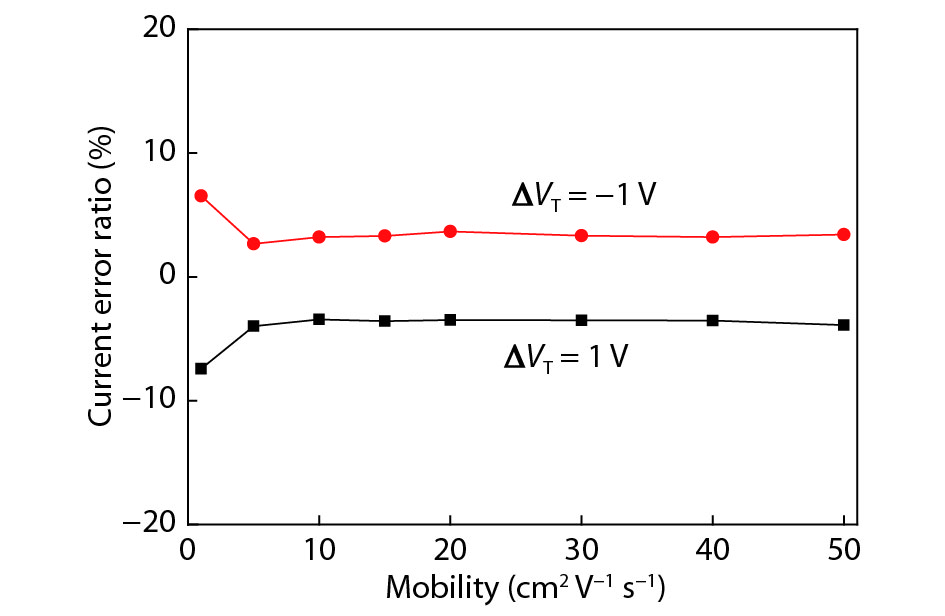


Table 1. Values of parameters in the RPI model related to effective mobility.
| Parameter | Value |
| MUBAND (m2V−1s−1) | 2.11 |
| GAMMA | 0.95 |
| VAA (V) | 45 550 |
| VMIN (V) | 0.02 |
| DELTA | 24 |
| ALPHASAT | 1.0 |
| VT0 (V) | 0.5 |
| VFB (V) | −2.2 |
 DownLoad: CSV
Table 2. Design parameters of the proposed pixel circuit.
| Parameter | Value | Parameter | Value |
| VSCAN (V) | −5 to 20 | (W/L) TS1 (μm/μm) | 10/10 |
| VEM1 (V) | −5 to 20 | (W/L) TS2 (μm/μm) | 10/10 |
| VEM2 (V) | −5 to 20 | (W/L)TEM1 (μm/μm) | 10/10 |
| VDATA (V) | 5 to 10 | (W/L)TEM2 (μm/μm) | 10/10 |
| EVDD (V) | 15 | (W/L)TD (μm/μm) | 50/10 |
| EVSS (V) | −3 | CS (pF) | 0.3 |
| VREF (V) | 5 | COLED (pF) | 0.5 |
DownLoad: CSV
| [1] |
Mo Y, Kim M, Kang C, et al. Amorphous oxide TFT backplane for large size AMOLED TVs. SID 2010 Digest, 2010: 1037.
|
| [2] |
C Leng, C Wang, L Wang, et al. Separate frame compensated current-biased voltage-programmed active matrix organic light-emitting diode pixel. IEEE Electron Device Lett, 2014, 35(8): 847 doi: 10.1109/LED.2014.2329943
|
| [3] |
Kawashima S, Inoue S, Shiokawa M, et al. 13.3-in. 8K × 4K 664-ppi OLED display using CAAC-OS FETs. SID 2014 Digest, 2014: 627
|
| [4] |
X Guo, S Silva. Investigation on the current nonuniformity in current-mode TFT active-matrix display pixel circuitry. IEEE Trans Electron Devices, 2005, 52(11): 2379. doi: 10.1109/TED.2005.857936
|
| [5] |
X Guo, S Silva, A simple and effective approach to improve the output linearity of switched-current AMOLED pixel circuitry. IEEE Electron Device Lett, 2007, 28(10): 887. doi: 10.1109/LED.2007.904905
|
| [6] |
M Wang, M Wong. An effective channel mobility-based analytical on-current model for polycrystalline silicon thin-film transistors, IEEE Trans Electron Devices, 2007, 54(4): 869. doi: 10.1109/TED.2007.891248
|
| [7] |
A Nathan, A Kumar, K Sakariya, et al. Amorphous silicon thin film transistor circuit integration for organic LED displays on glass and plastic. IEEE J Solid-State Circuits, 2004, 39(9): 1477. doi: 10.1109/JSSC.2004.829373
|
| [8] |
A Nathan, S Lee, S Jeon, et al. Amorphous Oxide semiconductor TFTs for displays and imaging. IEEE J Display Technol, 2014, 10(11): 917. doi: 10.1109/JDT.2013.2292580
|
| [9] |
X He, L Wang, X Xiao, et al. Implementation of fully self-aligned homojunction double-gate a-IGZO TFTs. IEEE Electron Device Lett. 2014, 35(9): 927. doi: 10.1109/LED.2014.2336232
|
| [10] |
Y Kim, H Kang, G Kim, et al. Improvement in device performance of vertical thin-film transistors using atomic layer deposited IGZO channel and polyimide spacer. IEEE Electron Device Lett. 2017, 38(10): 1387. doi: 10.1109/LED.2017.2736000
|
| [11] |
Y Tian, D Han, S Zhang, et al. High-performance dual-layer channel indium gallium zinc oxide thin-film transistors fabricated in different oxygen contents at low temperature. Jpn J Appl Phys, 2014, 53: 04EF07. doi: 10.7567/JJAP.53.04EF07
|
| [12] |
A Kumar, A Nathan, G Jabbour, Does TFT mobility impact pixel size in AMOLED backplanes, IEEE Trans Electron Devices, 2005, 52(11): 2386. doi: 10.1109/TED.2005.857937
|
| [13] |
Jang Y, Kim D, Choi W, et al. Internal compensation type OLED display using high mobility oxide TFT. SID 2017 Digest, 2017: 76
|
| [14] |
M Estrada, A Cerdeira, A Ortiz-Conde, et al. Extraction method for polycrystalline TFT above and below threshold model parameters. Solid-State Electron, 2002, 46: 2295. doi: 10.1016/S0038-1101(02)00186-7
|
| [15] |
P Servati, D Striakhilev, A Nathan. Above-threshold parameter extraction and modeling for amorphous silicon thin-film transistors. IEEE Trans Electron Devices, 2003, 50(11): 2227. doi: 10.1109/TED.2003.818156
|
| [16] |
K Ryu, I Kymissis, V Bulovic, et al. Direct extraction of mobility in pentacene OFETs using C–V and I–V measurements. IEEE Electron Device Lett. 2005, 26(10): 716. doi: 10.1109/LED.2005.854394
|
| [17] |
M Estrada, A Cerdeira, J Puigdollers, et al. Accurate modeling and parameter extraction method for organic TFTs. Solid-State Electron, 2005, 49: 1009. doi: 10.1016/j.sse.2005.02.004
|
| [18] |
Yang M F. Amorphous silicon thin film transistor models and pixel circuits for AMOLED displays. PhD Thesis, University of Waterloo, 2014
|
| [19] |
Holly Claudia Slade. Device and material characterization and analytic modeling of amorphous silicon thin film transistors. PhD Thesis, University of Virginia, 1997
|
| [20] |
SMART SPICE User’s manual, SILVACO Inc. 2014
|
| [21] |
W Aerts, S Verlaak, P Heremans. Design of an organic pixel addressing circuit for an active-matrix OLED display. IEEE Trans Electron Devices, 2002, 49(12): 2124. doi: 10.1109/TED.2002.805565
|


Article views: 5907 Times PDF downloads: 246 Times Cited by: 0 Times
Received: 16 October 2017 Revised: 15 November 2018 Online: Accepted Manuscript: 03 January 2019Uncorrected proof: 04 January 2019Published: 01 February 2019
| Citation: |
Congwei Liao. Mobility impact on compensation performance of AMOLED pixel circuit using IGZO TFTs[J]. Journal of Semiconductors, 2019, 40(2): 022403. doi: 10.1088/1674-4926/40/2/022403
****
C W Liao, Mobility impact on compensation performance of AMOLED pixel circuit using IGZO TFTs[J]. J. Semicond., 2019, 40(2): 022403. doi: 10.1088/1674-4926/40/2/022403.

|
| [1] |
Mo Y, Kim M, Kang C, et al. Amorphous oxide TFT backplane for large size AMOLED TVs. SID 2010 Digest, 2010: 1037.
|
| [2] |
C Leng, C Wang, L Wang, et al. Separate frame compensated current-biased voltage-programmed active matrix organic light-emitting diode pixel. IEEE Electron Device Lett, 2014, 35(8): 847 doi: 10.1109/LED.2014.2329943
|
| [3] |
Kawashima S, Inoue S, Shiokawa M, et al. 13.3-in. 8K × 4K 664-ppi OLED display using CAAC-OS FETs. SID 2014 Digest, 2014: 627
|
| [4] |
X Guo, S Silva. Investigation on the current nonuniformity in current-mode TFT active-matrix display pixel circuitry. IEEE Trans Electron Devices, 2005, 52(11): 2379. doi: 10.1109/TED.2005.857936
|
| [5] |
X Guo, S Silva, A simple and effective approach to improve the output linearity of switched-current AMOLED pixel circuitry. IEEE Electron Device Lett, 2007, 28(10): 887. doi: 10.1109/LED.2007.904905
|
| [6] |
M Wang, M Wong. An effective channel mobility-based analytical on-current model for polycrystalline silicon thin-film transistors, IEEE Trans Electron Devices, 2007, 54(4): 869. doi: 10.1109/TED.2007.891248
|
| [7] |
A Nathan, A Kumar, K Sakariya, et al. Amorphous silicon thin film transistor circuit integration for organic LED displays on glass and plastic. IEEE J Solid-State Circuits, 2004, 39(9): 1477. doi: 10.1109/JSSC.2004.829373
|
| [8] |
A Nathan, S Lee, S Jeon, et al. Amorphous Oxide semiconductor TFTs for displays and imaging. IEEE J Display Technol, 2014, 10(11): 917. doi: 10.1109/JDT.2013.2292580
|
| [9] |
X He, L Wang, X Xiao, et al. Implementation of fully self-aligned homojunction double-gate a-IGZO TFTs. IEEE Electron Device Lett. 2014, 35(9): 927. doi: 10.1109/LED.2014.2336232
|
| [10] |
Y Kim, H Kang, G Kim, et al. Improvement in device performance of vertical thin-film transistors using atomic layer deposited IGZO channel and polyimide spacer. IEEE Electron Device Lett. 2017, 38(10): 1387. doi: 10.1109/LED.2017.2736000
|
| [11] |
Y Tian, D Han, S Zhang, et al. High-performance dual-layer channel indium gallium zinc oxide thin-film transistors fabricated in different oxygen contents at low temperature. Jpn J Appl Phys, 2014, 53: 04EF07. doi: 10.7567/JJAP.53.04EF07
|
| [12] |
A Kumar, A Nathan, G Jabbour, Does TFT mobility impact pixel size in AMOLED backplanes, IEEE Trans Electron Devices, 2005, 52(11): 2386. doi: 10.1109/TED.2005.857937
|
| [13] |
Jang Y, Kim D, Choi W, et al. Internal compensation type OLED display using high mobility oxide TFT. SID 2017 Digest, 2017: 76
|
| [14] |
M Estrada, A Cerdeira, A Ortiz-Conde, et al. Extraction method for polycrystalline TFT above and below threshold model parameters. Solid-State Electron, 2002, 46: 2295. doi: 10.1016/S0038-1101(02)00186-7
|
| [15] |
P Servati, D Striakhilev, A Nathan. Above-threshold parameter extraction and modeling for amorphous silicon thin-film transistors. IEEE Trans Electron Devices, 2003, 50(11): 2227. doi: 10.1109/TED.2003.818156
|
| [16] |
K Ryu, I Kymissis, V Bulovic, et al. Direct extraction of mobility in pentacene OFETs using C–V and I–V measurements. IEEE Electron Device Lett. 2005, 26(10): 716. doi: 10.1109/LED.2005.854394
|
| [17] |
M Estrada, A Cerdeira, J Puigdollers, et al. Accurate modeling and parameter extraction method for organic TFTs. Solid-State Electron, 2005, 49: 1009. doi: 10.1016/j.sse.2005.02.004
|
| [18] |
Yang M F. Amorphous silicon thin film transistor models and pixel circuits for AMOLED displays. PhD Thesis, University of Waterloo, 2014
|
| [19] |
Holly Claudia Slade. Device and material characterization and analytic modeling of amorphous silicon thin film transistors. PhD Thesis, University of Virginia, 1997
|
| [20] |
SMART SPICE User’s manual, SILVACO Inc. 2014
|
| [21] |
W Aerts, S Verlaak, P Heremans. Design of an organic pixel addressing circuit for an active-matrix OLED display. IEEE Trans Electron Devices, 2002, 49(12): 2124. doi: 10.1109/TED.2002.805565
|

 WeChat ID
Journal of Semiconductors © 2017 All Rights Reserved 京ICP备05085259号-2


