| Citation: |
Xiaorang Tian, Peide Han, Guanchao Zhao, Rong Yang, Liwei Li, Yuan Meng, Ted Guo. Pyramid size control and morphology treatment for high-efficiency silicon heterojunction solar cells[J]. Journal of Semiconductors, 2019, 40(3): 032703. doi: 10.1088/1674-4926/40/3/032703
****
X R Tian, P D Han, G C Zhao, R Yang, L W Li, Y Meng, T Guo, Pyramid size control and morphology treatment for high-efficiency silicon heterojunction solar cells[J]. J. Semicond., 2019, 40(3): 032703. doi: 10.1088/1674-4926/40/3/032703.
|
Pyramid size control and morphology treatment for high-efficiency silicon heterojunction solar cells
DOI: 10.1088/1674-4926/40/3/032703
More Information
-
Abstract
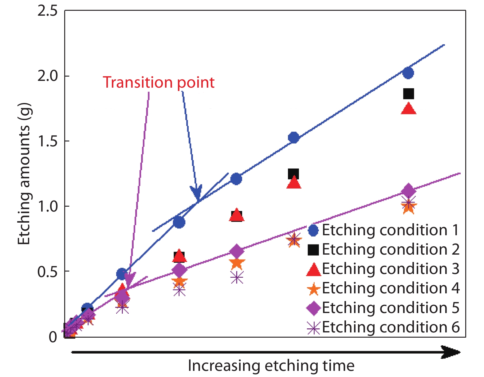
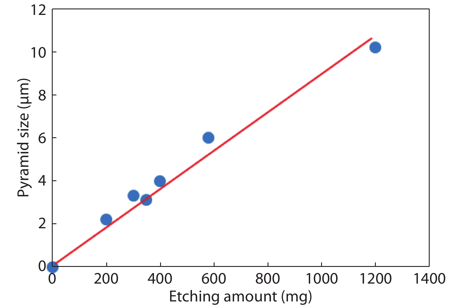
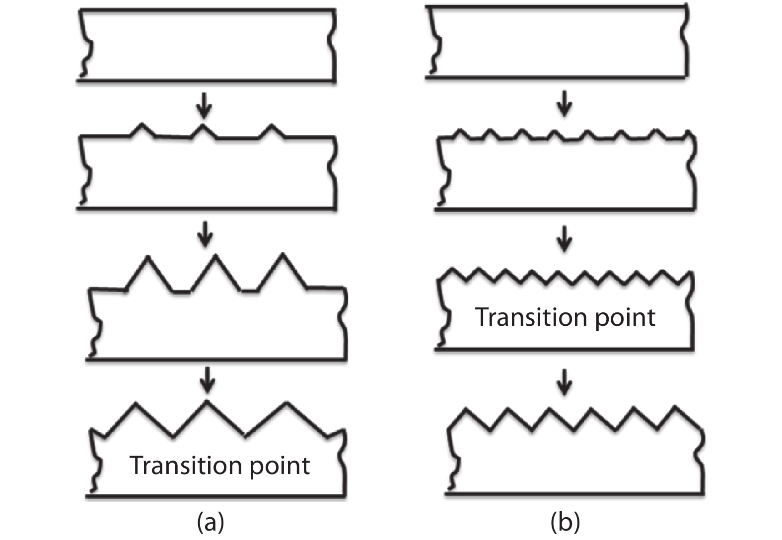
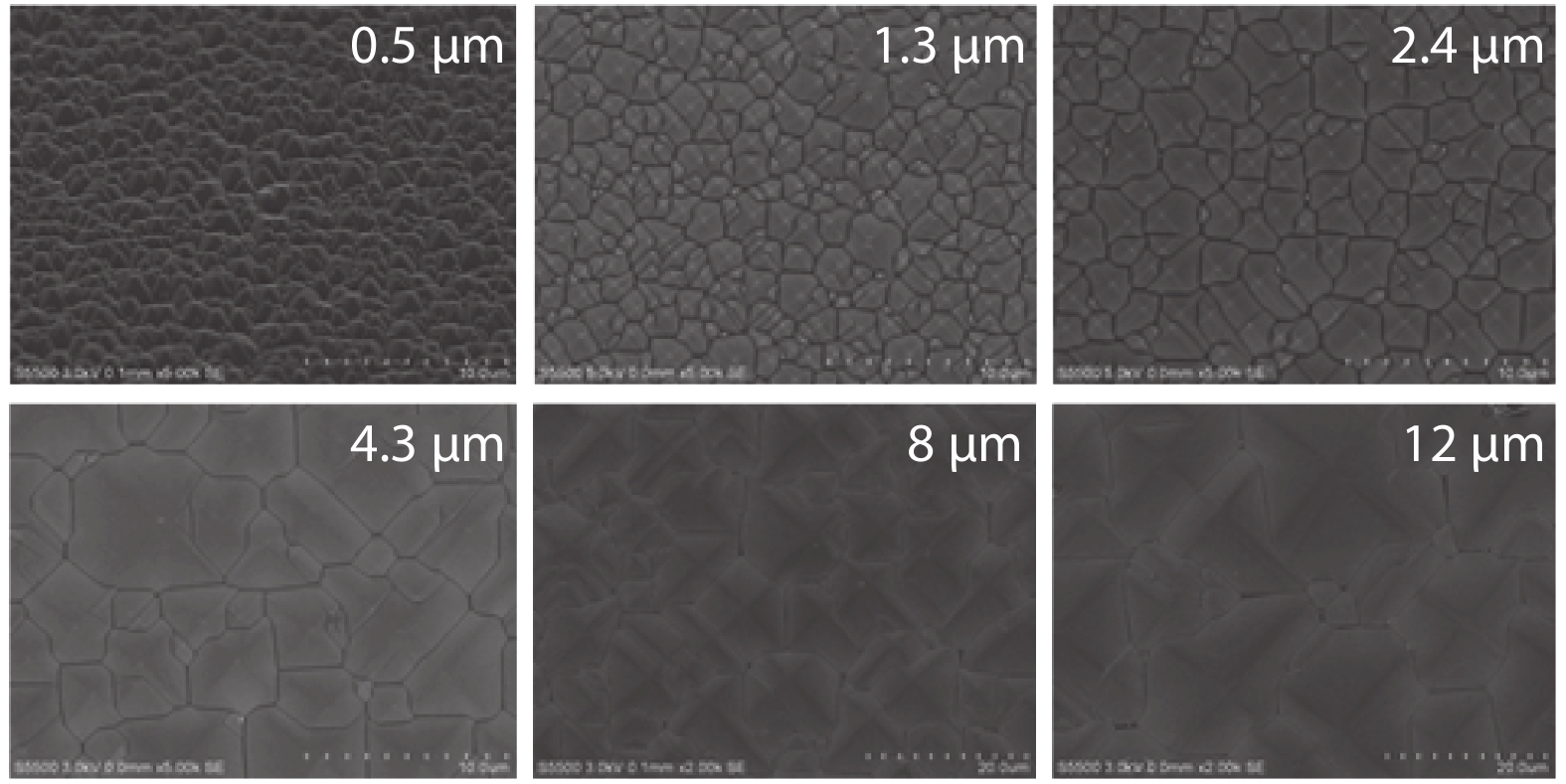
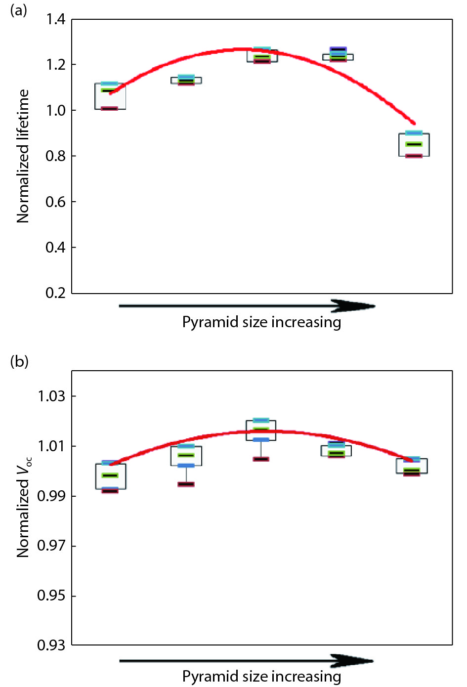
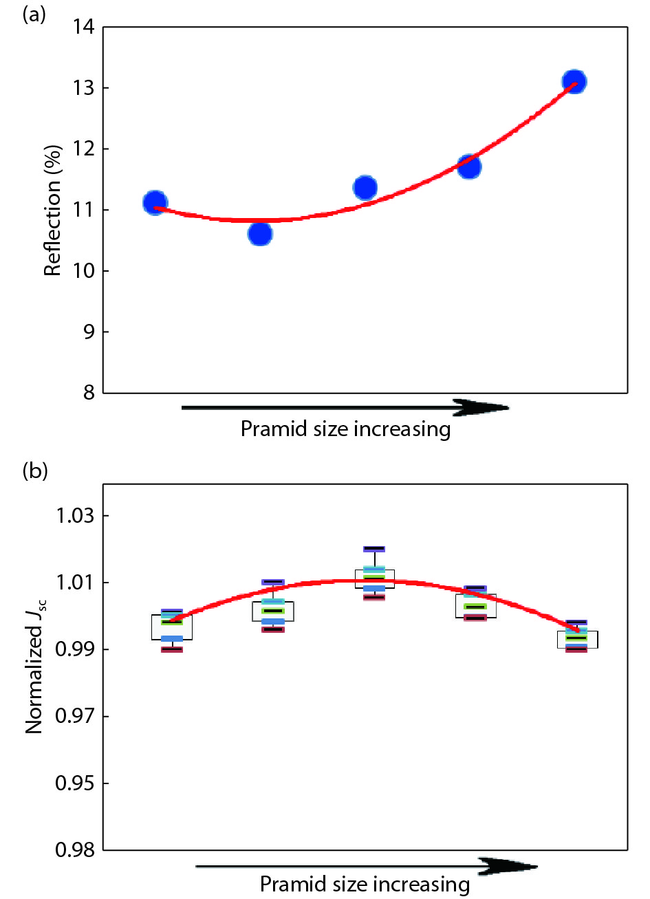
This paper investigates the formation process of surface pyramid and etching characteristics during the texturing process of mono-crystalline silicon wafers. It is found that there is an etch rate transition point in alkaline anisotropic etching when {100} plane-dominated etch turns to {111} plane-dominated etch, and the pyramid size has a strong linear correlation with the etch amount at the transition point. Several techniques were developed to control the pyramid size by monitoring and adjusting the etching amount. A wide range of average pyramid sizes were successfully achieved, from 0.5 to 12 μm. The experiments of the pyramid size on the light reflectance, the minority carrier lifetime (MCLT), and the performance of silicon heterojunction (SHJ) solar cells were carried out and analyzed. A desirable range of pyramid sizes was empirically determined by our investigation. In order to reduce the density states on the texturing surface, the wet-chemical smoothing treatment was also investigated. The smoothing treatment improves the passivation quality and the performance of the solar cells. Through pyramid size control and morphology treatment, together with the amorphous silicon (a-Si:H) deposition improvement, and electrode optimization, high performance of SHJ solar cells has been achieved, up to conversion efficiency 23.6%.-
Keywords:
- pyramid size,
- silicon,
- heterojunction,
- passivation
-
References
[1] Angermann H, Conrad E, Korte L, et al. Passivation of textured substrates for a-Si:H/c-Si hetero-junction solar cells: Effect of wet-chemical smoothing and intrinsic a-Si:H interlayer. Mater Sci Eng B, 2010, 159: 219 doi: 10.1016/j.mseb.2008.10.044[2] Rocío B, Nieves G, Cárabe J, et al. Optimisation of NaOH texturisation process of silicon wafers for heterojunction solar-cells applications. Solar Energy, 2012, 86: 845 doi: 10.1016/j.solener.2011.12.013[3] Simeon C, Finch B. Reflection of normally incident light from silicon solar cells with pyramidal texture. Prog Photovolt: Res Appl, 2011, 19: 406 doi: 10.1002/pip.1050[4] Hiroyuki F, Michio K. Impact of epitaxial growth at the heterointerface of a-Si:H/c-Si/a-Si:H/c-Si solar cells. Appl Phys Lett, 2007, 90: 013503. doi: 10.1063/1.2426900[5] Kegela J, Angermann H, Stürzebecher U, et al. Over 20% conversion efficiency on silicon heterojunction solar cells by IPA-free substrate texturization. Appl Surf Sci, 2014, 301: 56 doi: 10.1016/j.apsusc.2014.01.183[6] Kegela J, Angermann H, Stürzebecher U, et al. IPA-free textured a-Si:H/c-Si heterojunction solar cells exceeding 20% efficiency. Proc 28th EU PVSEC, 2013: 1093[7] Bonilla R S, Hoex B, Hamer P, et al. Dielectric surface passivation for silicon solar cells: A review. Phys Status Solidi, 2017, 7: 214 doi: 10.1002/pssa.201700293[8] Edwards M, Bowden S, Das U. Effect of texturing and surface preparation on lifetime and cell performance in heterojunction silicon solar cells. Sol Energy Mater Sol Cells, 2008, 92: 1373 doi: 10.1016/j.solmat.2008.05.011[9] Mrazkova Z, Sobkowicz I P, Foldyna M, et al. Optical properties and performance of pyramidal texture silicon heterojunction solar cells: Key role of vertex angles. Prog Photovolt: Res Appl, 2018, 26: 369 doi: 10.1002/pip.v26.6[10] Nagel H, Berge C, Aberle A G. Generalized analysis of quasi-steady-state and quasi-transient measurements of carrier lifetimes in semiconductors. J Appl Phys, 1999, 86: 6218 doi: 10.1063/1.371633[11] Siah S C, Berge C, Aberle A G, et al. Proof-of-concept framework to separate recombination processes in thin silicon wafers using transient free-carrier absorption spectroscopy. J Appl Phys, 2015, 117: 662 doi: 10.1063/1.4914160[12] Fesquet L, Olibet S, Lacoste J D, et al. Modification of textured silicon wafer surface morphology for fabrication of heterojunction solar cell with open circuit voltage over 700 mV. Photovoltaic Specialists Conference, 2009: 754[13] Wolf S D, Kondo D. Abruptness of a-Si:H/c-Si interface revealed by carrier lifetime measurements. Applied Physics Lefters, 2007, 90: 042111 doi: 10.1063/1.2432297[14] Lacoste J D, Roca C P. Toward a better physical understanding of a-Si:H/c-Si heterojunction solar cells. J Appl Phys, 2009, 105: 345 doi: 10.1063/1.3091283[15] Das U K, Burrows M Z, Lu M, et al. Surface passivation and heterojunction cells on Si (100) and (111) wafers using dc and rf plasma deposited Si:H thin films. Appl Phys Lett, 2008, 92: 481 doi: 10.1063/1.2857465[16] Stegemann B, Kegel J, Mews M, et al. Passivation of textured silicon wafers: influence of pyramid size distribution, a-Si:H deposition temperature, and post-treatment. Energy Procedia, 2013, 38: 881 doi: 10.1016/j.egypro.2013.07.360[17] Lien S Y, Yang C H, Lin Y S, et al. Optimization of textured structure on crystalline silicon wafer for heterojunction solar cell. Mater Chem Phys, 2012, 133: 63 doi: 10.1016/j.matchemphys.2011.12.052[18] Stegemann B, Kegel J, Gref O. Conditioning of textured silicon solar cell substrates by wet-chemical treatments. 27th EUPVSEC, 2011: 547 -
Proportional views


 DownLoad:
