J. Semicond. > 2019, Volume 40 > Issue 4 > 042402

ARTICLES

Improving the data retention of phase change memory by using a doping element in selected Ge2Sb2Te5

Yaoyao Lu1, 2, Daolin Cai1, , Yifeng Chen1, Shuai Yan1, 2, Lei Wu1, 2, Yuanguang Liu1, 2, Yang Li1, 2 and Zhitang Song1

+ Author Affiliations

 Corresponding author: Daolin Cai, Email: caidl@mail.sim.ac.cn

DOI: 10.1088/1674-4926/40/4/042402

PDF

Turn off MathJax

Abstract: The crystallization characteristics of a ubiquitous T-shaped phase change memory (PCM) cell, under SET current pulse and very small disturb current pulse, have been investigated by finite element modelling. As analyzed in this paper, the crystallization region under SET current pulse presents first on the corner of the bottom electron contact (BEC) and then promptly forms a filament shunting down the amorphous phase to achieve the low-resistance state, whereas the tiny disturb current pulse accelerates crystallization at the axis of symmetry in the phase change material. According to the different crystallization paths, a new structure of phase change material layer is proposed to improve the data retention for PCM without impeding SET operation. This structure only requires one or two additional process steps to dope nitrogen element in the center region of phase change material layer to increase the crystallization temperature in this confined region. The electrical-thermal characteristics of PCM cells with incremental doped radius have been analyzed and the best performance is presented when the doped radius is equal to the radius of the BEC.

Key words: phase change memorycrystallization processSET current pulsesmall disturb current pulsefinite element simulation


[1]
Lai S. Current status of the phase change memory and its future. IEEE International Electron Devices Meeting, 2003, 255 doi: 10.1109/IEDM.2003.1269271
[2]
Ovshinsky S R. Reversible electrical switching phenomena in disordered structures. Phys Rev Lett, 1968, 21, 1450 doi: 10.1103/PhysRevLett.21.1450
[3]
Sun Z M, Zhou J, Ahuja R. Structure of phase change materials for data storage. Phys Rev Lett, 2006, 96, 055507 doi: 10.1103/PhysRevLett.96.055507
[4]
Raoux S, Welnic W, Ielmini D. Phase change materials and their application to nonvolatile memories. Chem Rev, 2009, 110, 240 doi: 10.1021/cr900040x
[5]
Kohary K, Wright C D. Electric field induced crystallization in phase-change materials for memory applications. Appl Phys Lett, 2011, 98, 223102 doi: 10.1063/1.3595408
[6]
Li J M, Yang H M, Lim K G. Field-dependent activation energy of nucleation and switching in phase change memory. Appl Phys Lett, 2012, 100, 263501 doi: 10.1063/1.4731289
[7]
Lee B S, Bishop S G. phase change materials: optical and electrical properties of phase change materials. In: Springer Science + Business Media. New York, 2009, 189
[8]
Cai D L, Chen H P, Wang Q, et al. An 8-mb phase-change random access memory chip based on a resistor-on-via-stacked-plug storage cell. IEEE Electron Device Lett, 2012, 33, 1270 doi: 10.1109/LED.2012.2204952
[9]
Liu Y, Song Z T, Ling Y, et al. Three-dimensional numerical simulation of phase-change memory cell with probe like bottom electrode structure. Jpn J Appl Phys, 2009, 48, 024502 doi: 10.1143/JJAP.48.024502
[10]
Xu Z, Liu B, Chen Y F, et al. The improvement of nitrogen doped Ge2Sb2Te5 on the phase change memory resistance distributions. Solid-State Electron, 2016, 116, 119 doi: 10.1016/j.sse.2015.11.001
[11]
Johnson W A, Mehl R F. Reaction kinetics in processes of nucleation and growth. Trans Metall Soc AIME, 1939, 135, 416
[12]
Volmer M, Weber A. Keimbildung in übersättigten Gebilden. Zeitschrift für physikalische Chemie, 1926, 119, 227 doi: 10.1515/zpch-1926-11927
[13]
Senkader S, Wright C D. Models for phase-change of Ge2Sb2Te5 in optical and electrical memory devices. J Appl Phys Lett, 2004, 95(2), 504 doi: 10.1063/1.1633984
[14]
Bae J H, Kim B G, Byeon D S, et al. Simulation for thickness change of PRAM recording layer. J Ceram Soc Jpn, 2009, 117(5), 588 doi: 10.2109/jcersj2.117.588
[15]
Gong Y F, Song Z T, Ling Y, et al. Simulation of voltage SET operation in phase-change random access memories with heater addition and ring-type contactor for low-power consumption by finite element modeling. Chin Phys Lett, 2010, 27, 068501 doi: 10.1088/0256-307X/27/6/068501
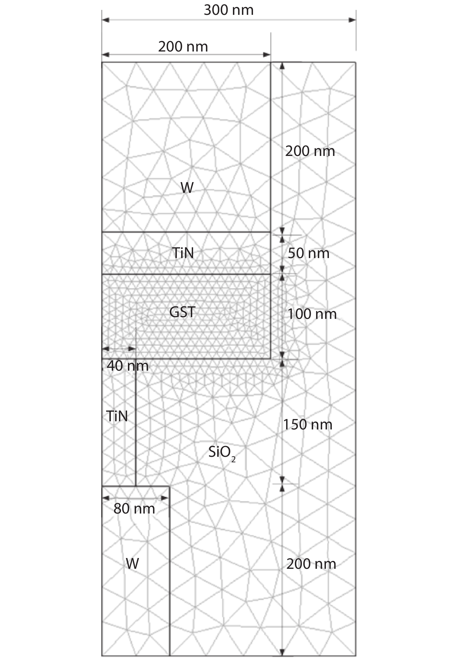
Fig. 1.  (Color online) Geometries and schematic cross section of the T-shaped PCM cell.

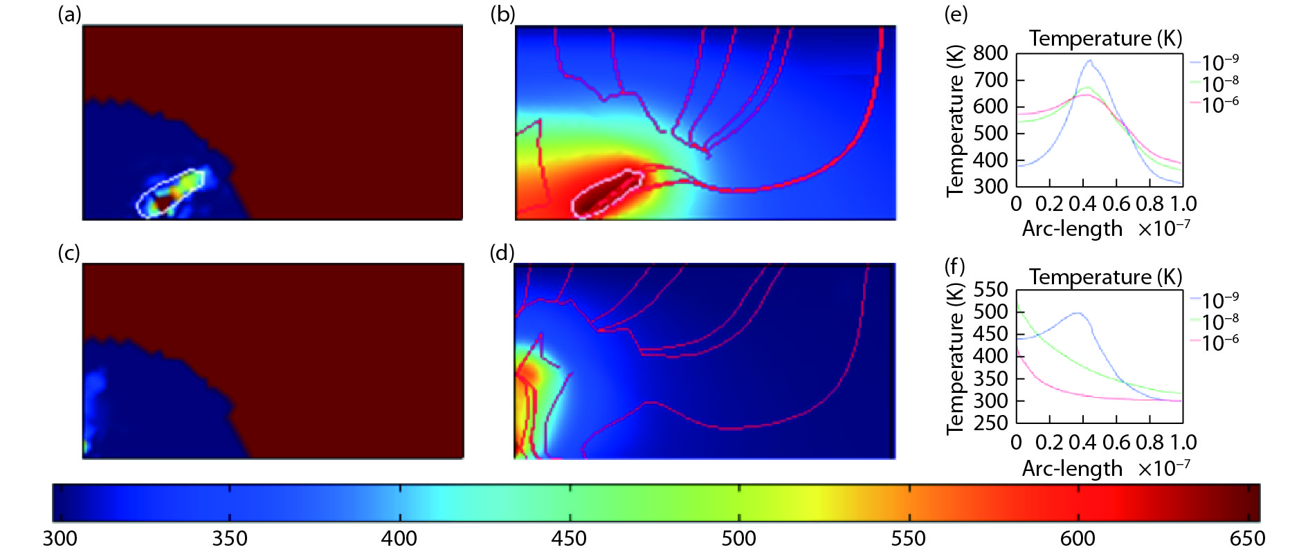
Fig. 2.  (Color online) The crystalline domain (light color) among amorphous phase (dark blue) under current pulses of (a) 0.5 mA/1 μs and (b) 0.01 mA/1 μs; the temperature distributions and current density distributions under current pulses of (c) 0.5 mA/1 μs and (d) 0.01 mA/1 μs; the temperature values along horizontal direction (r-axis) under current pulses of (e) 0.5 mA/1 μs and (f) 0.01 mA/1 μs, the time points vary from 1 ns (blue line) to 1 μs (red line), the median time point is 10 ns (green line).

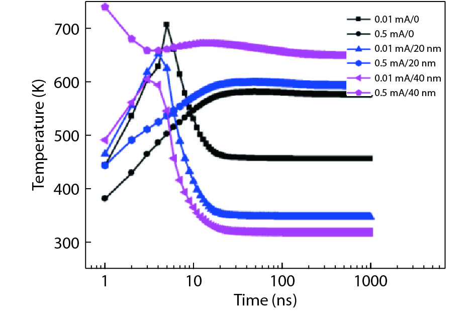
Fig. 3.  (Color online) Temperature profiles of selective points along horizontal direction (r-axis) during current pulse: lines are presented under current amplitude of 0.5 mA whereas solid symbols are presented under current amplitude of 0.01 mA; points at coordinate (z = 360 nm, r = 0 nm) are expressed in black, points at coordinate (z = 360 nm, r = 20 nm) are expressed in blue, and points at coordinate (z = 360 nm, r = 40 nm) are expressed in pink. To facilitate the observation and comparison, the figure zooms in 60 ns. The entire temperature profiles are showed in insert figure.

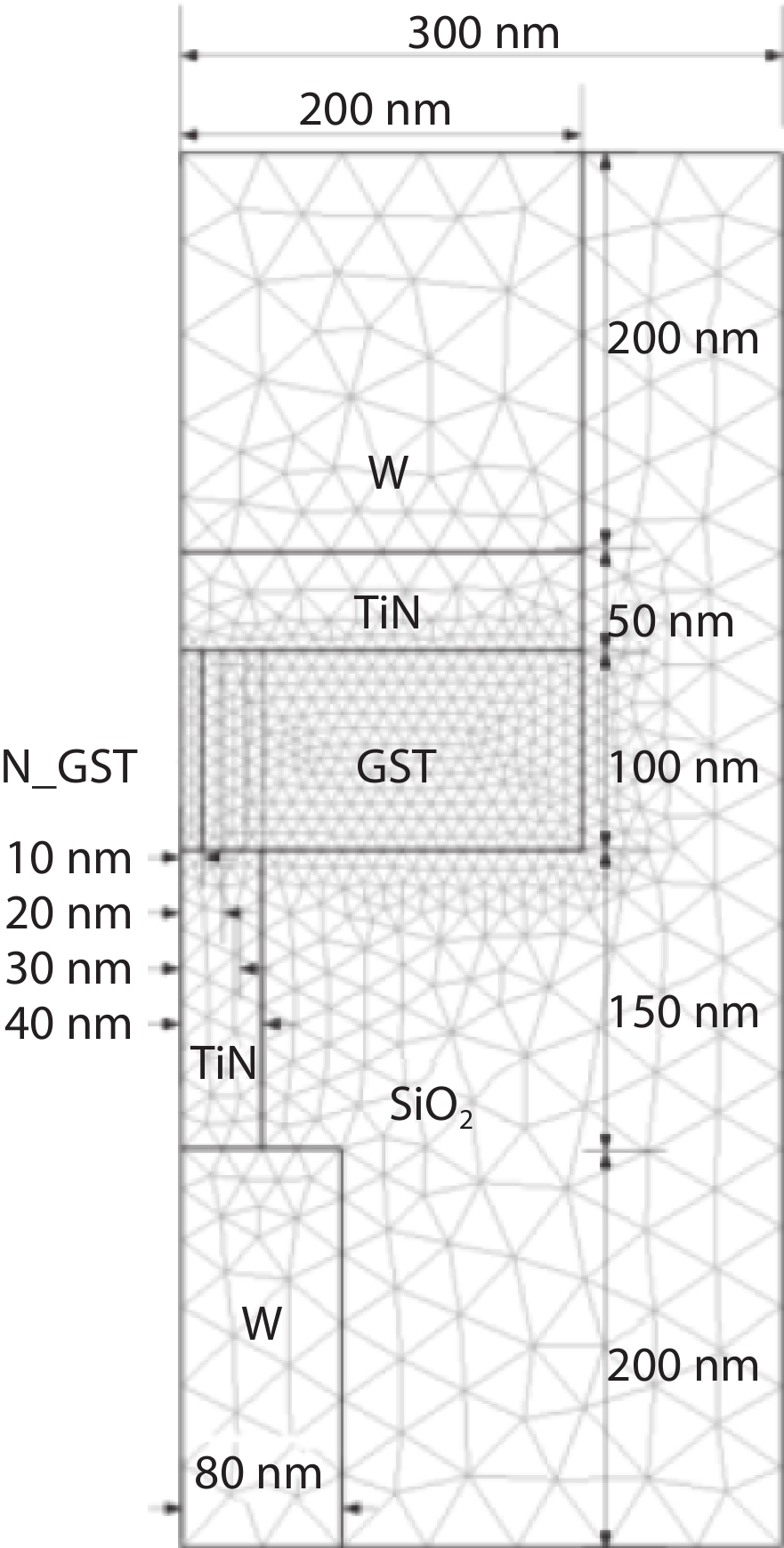
Fig. 4.  (Color online) Geometries and schematic cross sections of the PCM cell with incremental doped radius.

Fig. 5.  (Color online) The temperature distributions of RESET operation for the PCM cells with incremental doped radius.

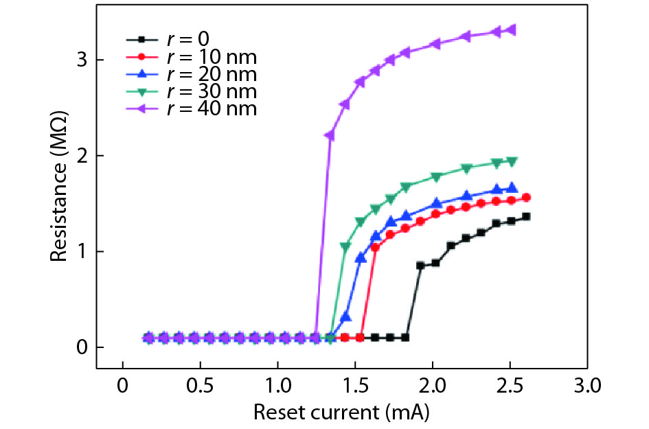
Fig. 6.  (Color online) Variations of resistance as a function of programming current amplitudes in RESET operations for the PCM cell with incremental doped radius.

Fig. 7.  (Color online) The temperature distributions and current density distributions of SET operation for the PCM cell with incremental doped radius.

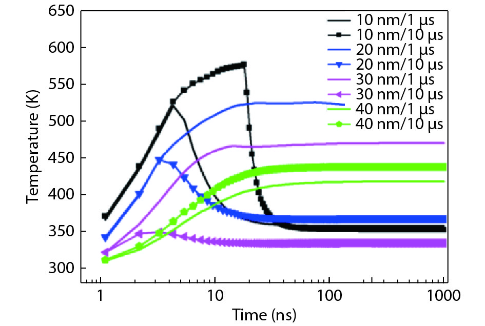
Fig. 9.  (Color online) Temperature profiles of the selective point (z = 380 nm, r = 0 nm) during current pulse: lines are presented under current duration of 1 μs whereas solid symbols are presented under current duration of 10 μs; the temperature changes of doped radius r = 10 nm are expressed in black, the temperature changes of doped radius r = 10 nm are expressed in blue, and the temperature changes of doped radius r = 10 nm are expressed in pink. To facilitate the observation and comparison, the figure zooms in the graphics within 80 ns.

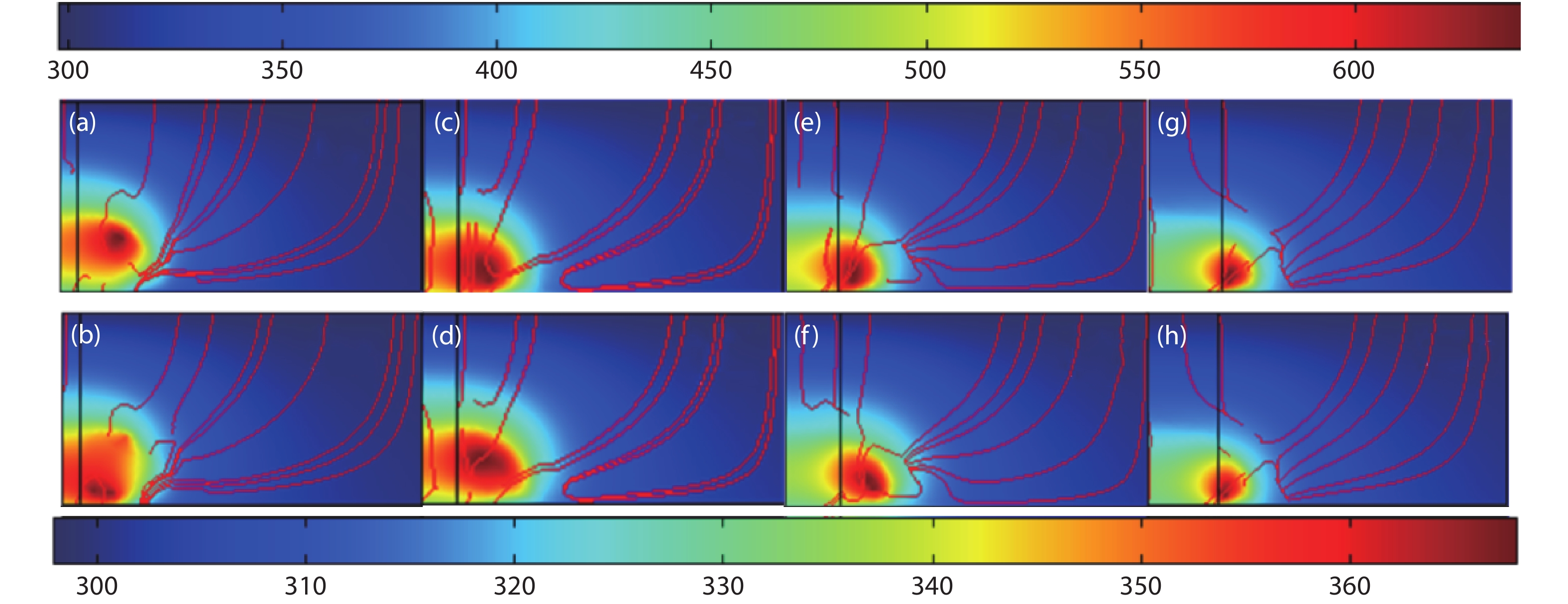
Fig. 8.  (Color online) The temperature distributions and current density distributions at electrical pulse of 0.01 mA and 1 μs of the PCM cells with different radius of doped regions: (a) r = 10 nm, (c) r = 20 nm, (e) r = 30 nm and (g) r = 40 nm. The results after increasing current pulse width to 10 μs, (b), (d), (f) and (h) correspond to (a), (c), (e) and (g) respectively.

Table 1.   Physical properties of materials used in numerical simulation.

ParameterElectrical conductivity σ–1∙m–1)Density ρ (kg/m3)Thermal conductivity k (W/(m∙K))Heatcapacity Cp (J/(kg∙K))
W1.75 × 10719 300178132
TiN contactor1 × 106540013784
GST crystalline1 × 10562000.5202
GST amorphous362000.5202
TiN (BEC)1 × 10554000.44784
SiO21 × 10−1423301.4730
DownLoad: CSV

Table 2.   The correlation coefficients of JMAK equation used in numerical simulation.

ParameterEAvnkB
Value2 × 1.6 × 10−19102211.38 × 10−23
DownLoad: CSV

Table 3.   Physical properties of N doped GST used in numerical simulation.

PrarmeterElectrical conductivity σ−1∙m−1)Density ρ (kg/m3)Thermal conductivity k (W/(m∙K))Heatcapacity Cp (J/(kg∙K))
N-GST crystalline2.3 × 10462000.5202
N-GST amorphous0.162000.5202
DownLoad: CSV
[1]
Lai S. Current status of the phase change memory and its future. IEEE International Electron Devices Meeting, 2003, 255 doi: 10.1109/IEDM.2003.1269271
[2]
Ovshinsky S R. Reversible electrical switching phenomena in disordered structures. Phys Rev Lett, 1968, 21, 1450 doi: 10.1103/PhysRevLett.21.1450
[3]
Sun Z M, Zhou J, Ahuja R. Structure of phase change materials for data storage. Phys Rev Lett, 2006, 96, 055507 doi: 10.1103/PhysRevLett.96.055507
[4]
Raoux S, Welnic W, Ielmini D. Phase change materials and their application to nonvolatile memories. Chem Rev, 2009, 110, 240 doi: 10.1021/cr900040x
[5]
Kohary K, Wright C D. Electric field induced crystallization in phase-change materials for memory applications. Appl Phys Lett, 2011, 98, 223102 doi: 10.1063/1.3595408
[6]
Li J M, Yang H M, Lim K G. Field-dependent activation energy of nucleation and switching in phase change memory. Appl Phys Lett, 2012, 100, 263501 doi: 10.1063/1.4731289
[7]
Lee B S, Bishop S G. phase change materials: optical and electrical properties of phase change materials. In: Springer Science + Business Media. New York, 2009, 189
[8]
Cai D L, Chen H P, Wang Q, et al. An 8-mb phase-change random access memory chip based on a resistor-on-via-stacked-plug storage cell. IEEE Electron Device Lett, 2012, 33, 1270 doi: 10.1109/LED.2012.2204952
[9]
Liu Y, Song Z T, Ling Y, et al. Three-dimensional numerical simulation of phase-change memory cell with probe like bottom electrode structure. Jpn J Appl Phys, 2009, 48, 024502 doi: 10.1143/JJAP.48.024502
[10]
Xu Z, Liu B, Chen Y F, et al. The improvement of nitrogen doped Ge2Sb2Te5 on the phase change memory resistance distributions. Solid-State Electron, 2016, 116, 119 doi: 10.1016/j.sse.2015.11.001
[11]
Johnson W A, Mehl R F. Reaction kinetics in processes of nucleation and growth. Trans Metall Soc AIME, 1939, 135, 416
[12]
Volmer M, Weber A. Keimbildung in übersättigten Gebilden. Zeitschrift für physikalische Chemie, 1926, 119, 227 doi: 10.1515/zpch-1926-11927
[13]
Senkader S, Wright C D. Models for phase-change of Ge2Sb2Te5 in optical and electrical memory devices. J Appl Phys Lett, 2004, 95(2), 504 doi: 10.1063/1.1633984
[14]
Bae J H, Kim B G, Byeon D S, et al. Simulation for thickness change of PRAM recording layer. J Ceram Soc Jpn, 2009, 117(5), 588 doi: 10.2109/jcersj2.117.588
[15]
Gong Y F, Song Z T, Ling Y, et al. Simulation of voltage SET operation in phase-change random access memories with heater addition and ring-type contactor for low-power consumption by finite element modeling. Chin Phys Lett, 2010, 27, 068501 doi: 10.1088/0256-307X/27/6/068501
  • Search

    Advanced Search >>

    GET CITATION

    shu

    Export: BibTex EndNote

    Article Metrics

    Article views: 3696 Times PDF downloads: 64 Times Cited by: 0 Times

    History

    Received: 19 October 2018 Revised: Online: Accepted Manuscript: 18 February 2019Uncorrected proof: 19 February 2019Published: 08 April 2019

    Catalog

      Email This Article

      User name:
      Email:*请输入正确邮箱
      Code:*验证码错误
      Yaoyao Lu, Daolin Cai, Yifeng Chen, Shuai Yan, Lei Wu, Yuanguang Liu, Yang Li, Zhitang Song. Improving the data retention of phase change memory by using a doping element in selected Ge2Sb2Te5[J]. Journal of Semiconductors, 2019, 40(4): 042402. doi: 10.1088/1674-4926/40/4/042402 ****Y Y Lu, D L Cai, Y F Chen, S Yan, L Wu, Y G Liu, Y Li, Z T Song, Improving the data retention of phase change memory by using a doping element in selected Ge2Sb2Te5[J]. J. Semicond., 2019, 40(4): 042402. doi: 10.1088/1674-4926/40/4/042402.
      Citation:
      Yaoyao Lu, Daolin Cai, Yifeng Chen, Shuai Yan, Lei Wu, Yuanguang Liu, Yang Li, Zhitang Song. Improving the data retention of phase change memory by using a doping element in selected Ge2Sb2Te5[J]. Journal of Semiconductors, 2019, 40(4): 042402. doi: 10.1088/1674-4926/40/4/042402 ****
      Y Y Lu, D L Cai, Y F Chen, S Yan, L Wu, Y G Liu, Y Li, Z T Song, Improving the data retention of phase change memory by using a doping element in selected Ge2Sb2Te5[J]. J. Semicond., 2019, 40(4): 042402. doi: 10.1088/1674-4926/40/4/042402.

      Improving the data retention of phase change memory by using a doping element in selected Ge2Sb2Te5

      DOI: 10.1088/1674-4926/40/4/042402
      More Information
      • Corresponding author: Email: caidl@mail.sim.ac.cn
      • Received Date: 2018-10-19
      • Published Date: 2019-04-01

      Catalog

        /

        DownLoad:  Full-Size Img  PowerPoint
        Return
        Return