


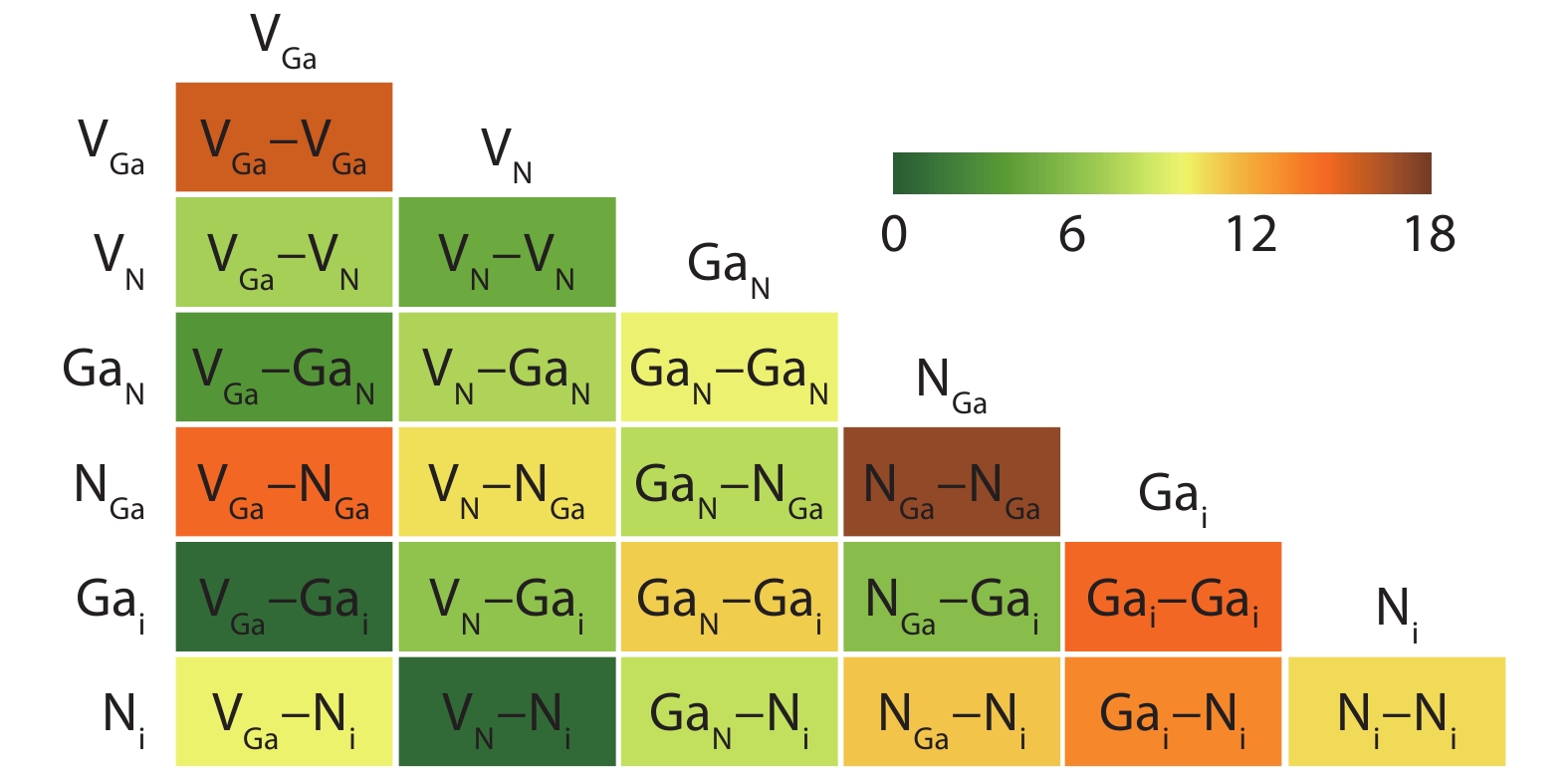
Fig. 1.
(Color online) The 21 defect-pairs that can be formed by two point defects in GaN. The color represents their formation energies in the neutral state (in Ga-rich GaN).
ARTICLES
He Li1, #, Menglin Huang1, # and Shiyou Chen1, 2,
Corresponding author: Shiyou Chen, chensy@ee.ecnu.edu.cn
Abstract: Using first-principles calculations, we explored all the 21 defect-pairs in GaN and considered 6 configurations with different defect-defect distances for each defect-pair. 15 defect-pairs with short defect–defect distances are found to be stable during structural relaxation, so they can exist in the GaN lattice once formed during the irradiation of high-energy particles. 9 defect-pairs have formation energies lower than 10 eV in the neutral state. The vacancy-pair VN–VN is found to have very low formation energies, as low as 0 eV in p-type and Ga-rich GaN, and act as efficient donors producing two deep donor levels, which can limit the p-type doping and minority carrier lifetime in GaN. VN–VN has been overlooked in the previous study of defects in GaN. Most of these defect-pairs act as donors and produce a large number of defect levels in the band gap. Their formation energies and concentrations are sensitive to the chemical potentials of Ga and N, so their influences on the electrical and optical properties of Ga-rich and N-rich GaN after irradiation should differ significantly. These results about the defect-pairs provide fundamental data for understanding the radiation damage mechanism in GaN and simulating the defect formation and diffusion behavior under irradiation.
Keywords: GaN, first-principles calculations, radiation damage, defect-pairs, point defects
| [1] |
Nakamura S, Mukai T, Senoh M. Candela-class high-brightness InGaN/AlGaN double-heterostructure blue-light-emitting diodes. Appl Phys Lett, 1994, 64(13), 1687 doi: 10.1063/1.111832
|
| [2] |
Kim M H, Schubert M F, Dai Q, et al. Origin of efficiency droop in GaN-based light-emitting diodes. Appl Phys Lett, 2007, 91(18), 183507 doi: 10.1063/1.2800290
|
| [3] |
Pimputkar S, Speck J S, DenBaars S P, et al. Prospects for LED lighting. Nat Photonics, 2009, 3(4), 180 doi: 10.1038/nphoton.2009.32
|
| [4] |
Sheppard S T, Doverspike K, Pribble W L, et al. High-power microwave GaN/AlGaN HEMTs on semi-insulating silicon carbide substrates. IEEE Electron Device Lett, 1999, 20(4), 161 doi: 10.1109/55.753753
|
| [5] |
Pearton S J, Deist R, Ren F, et al. Review of radiation damage in GaN-based materials and devices. J Vac Sci Technol A, 2013, 31(5), 050801 doi: 10.1116/1.4799504
|
| [6] |
Wang J, Mulligan P, Brillson L, et al. Review of using gallium nitride for ionizing radiation detection. Appl Phys Rev, 2015, 2(3), 031102 doi: 10.1063/1.4929913
|
| [7] |
Pearton S J, Ren F, Patrick E, et al. Review-ionizing radiation damage effects on GaN devices. ECS J Solid State Sci Technol, 2015, 5(2), Q35 doi: 10.1149/2.0251602jss
|
| [8] |
Pearton S J, Hwang Y S, Ren F. Radiation effects in GaN-based high electron mobility transistors. J Mater, 2015, 67(7), 1601 doi: 10.1007/s11837-015-1359-y
|
| [9] |
Khanna S M, Estan D, Houdayer A, et al. Proton radiation damage at low temperature in GaAs and GaN light-emitting diodes. IEEE Trans Nucl Sci, 2004, 51(6), 3585 doi: 10.1109/TNS.2004.839105
|
| [10] |
Lorenz K, Peres M, Franco N, et al. Radiation damage formation and annealing in GaN and ZnO. Proc SPIE, 2011
|
| [11] |
Polyakov A Y, Smirnov N B, Govorkov A V, et al. Neutron radiation effects in epitaxially laterally overgrown GaN films. J Electron Mater, 2007, 36(10), 1320 doi: 10.1007/s11664-007-0203-8
|
| [12] |
Pearton S J, Deist R, Polyakov A Y, et al. Radiation damage in GaN-based materials and devicesin. In: Advanced Energy Materials. Hoboken: John Wiley & Sons, Inc., 2014, 345
|
| [13] |
Nord J, Nordlund K, Keinonen J. Molecular dynamics study of damage accumulation in GaN during ion beam irradiation. Phys Rev B, 2003, 68(18), 184104 doi: 10.1103/PhysRevB.68.184104
|
| [14] |
Bryant F J, Webster E. Threshold energy for atomic displacement in cadmium telluride. Phys Status Solidi B, 1967, 21(1), 315 doi: 10.1002/pssb.19670210132
|
| [15] |
Bryant F J, Cox A F J, Frank F C. Experimental and calculated atomic displacement threshold energies for binary semiconductors. Proceedings of the Royal Society of London, Ser A, 1969, 310(1502), 319 doi: 10.1098/rspa.1969.0078
|
| [16] |
Von Bardeleben H J, Cantin J L, Gerstmann U, et al. Identification of the nitrogen split interstitial (N-N)N in GaN. Phys Rev Lett, 2012, 109(20), 206402 doi: 10.1103/PhysRevLett.109.206402
|
| [17] |
Van de Walle C G, Neugebauer J. First-principles calculations for defects and impurities: Applications to III-nitrides. J Appl Phys, 2004, 95(8), 3851 doi: 10.1063/1.1682673
|
| [18] |
Reshchikov M A, Morkoç H. Luminescence properties of defects in GaN. J Appl Phys, 2005, 97(6), 061301 doi: 10.1063/1.1868059
|
| [19] |
Lyons J L, Alkauskas A, Janotti A, et al. First-principles theory of acceptors in nitride semiconductors. Phys Status Solidi B, 2015, 252(5), 900 doi: 10.1002/pssb.201552062
|
| [20] |
Lyons J L, Van de Walle C G. Computationally predicted energies and properties of defects in GaN. npj Comp Mater, 2017, 3(1), 12 doi: 10.1038/s41524-017-0014-2
|
| [21] |
Polyakov A Y, Lee I H. Deep traps in GaN-based structures as affecting the performance of GaN devices. Mater Sci Eng R, 2015, 94, 1 doi: 10.1016/j.mser.2015.05.001
|
| [22] |
Mattila T, Nieminen R M. Point-defect complexes and broadband luminescence in GaN and AlN. Phys Rev B, 1997, 55(15), 9571 doi: 10.1103/PhysRevB.55.9571
|
| [23] |
Diallo I C, Demchenko D O. Native Point defects in GaN: a hybrid-functional study. Phys Rev Appl, 2016, 6(6), 064002 doi: 10.1103/PhysRevApplied.6.064002
|
| [24] |
Li Y G, Yang Y, Short M P, et al. IM3D: A parallel Monte Carlo code for efficient simulations of primary radiation displacements and damage in 3D geometry. Sci Rep, 2015, 5(1), 18130 doi: 10.1038/srep18130
|
| [25] |
Sham L J. Self-consistent equations including exchange and correlation effects. Phys Rev, 1965, 140(4A), A1138 doi: 10.1103/PhysRev.140.A1133
|
| [26] |
Kresse G, Joubert D. From ultrasoft pseudopotentials to the projector augmented-wave method. Phys Rev B, 1999, 59(3), 1758 doi: 10.1103/PhysRevB.59.1758
|
| [27] |
Blöchl P E. Projector augmented-wave method. Phys Rev B, 1994, 50(24), 17953 doi: 10.1103/PhysRevB.50.17953
|
| [28] |
Kresse G, Furthmüller J. Efficient iterative schemes for ab initio total-energy calculations using a plane-wave basis set. Phys Rev B, 1996, 54(16), 11169 doi: 10.1103/PhysRevB.54.11169
|
| [29] |
Perdew J P, Burke K, Ernzerhof M. Generalized gradient approximation made simple. Phys Rev Lett, 1996, 77(18), 3865 doi: 10.1103/PhysRevLett.77.3865
|
| [30] |
Heyd J, Scuseria G E, Ernzerhof M. Erratum: “Hybrid functionals based on a screened Coulomb potential” [J. Chem. Phys. 118, 8207(2003)]. J Chem Phys, 2006, 124(21), 219906 doi: 10.1063/1.2204597
|
| [31] |
Heyd J, Scuseria G E, Ernzerhof M. Hybrid functionals based on a screened Coulomb potential. J Chem Phys, 2003, 118(18), 8207 doi: 10.1063/1.1564060
|
| [32] |
Monemar B. Fundamental energy gap of GaN from photoluminescence excitation spectra. Phys Rev B, 1974, 10(2), 676 doi: 10.1103/PhysRevB.10.676
|
| [33] |
Lany S, Zunger A. Assessment of correction methods for the band-gap problem and for finite-size effects in supercell defect calculations: Case studies for ZnO and GaAs. Phys Rev B, 2008, 78(23), 235104 doi: 10.1103/PhysRevB.78.235104
|
| [34] |
Makov G, Payne M C. Periodic boundary conditions in ab initio calculations. Phys Rev B, 1995, 51(7), 4014 doi: 10.1103/PhysRevB.51.4014
|
| [35] |
Lyons J L, Janotti A, Walle C G. Carbon impurities and the yellow luminescence in GaN. Appl Phys Lett, 2010, 97(15), 152108 doi: 10.1063/1.3492841
|
| [36] |
Freysoldt C, Grabowski B, Hickel T, et al. First-principles calculations for point defects in solids. Rev Mod Phys, 2014, 86(1), 253 doi: 10.1103/RevModPhys.86.253
|

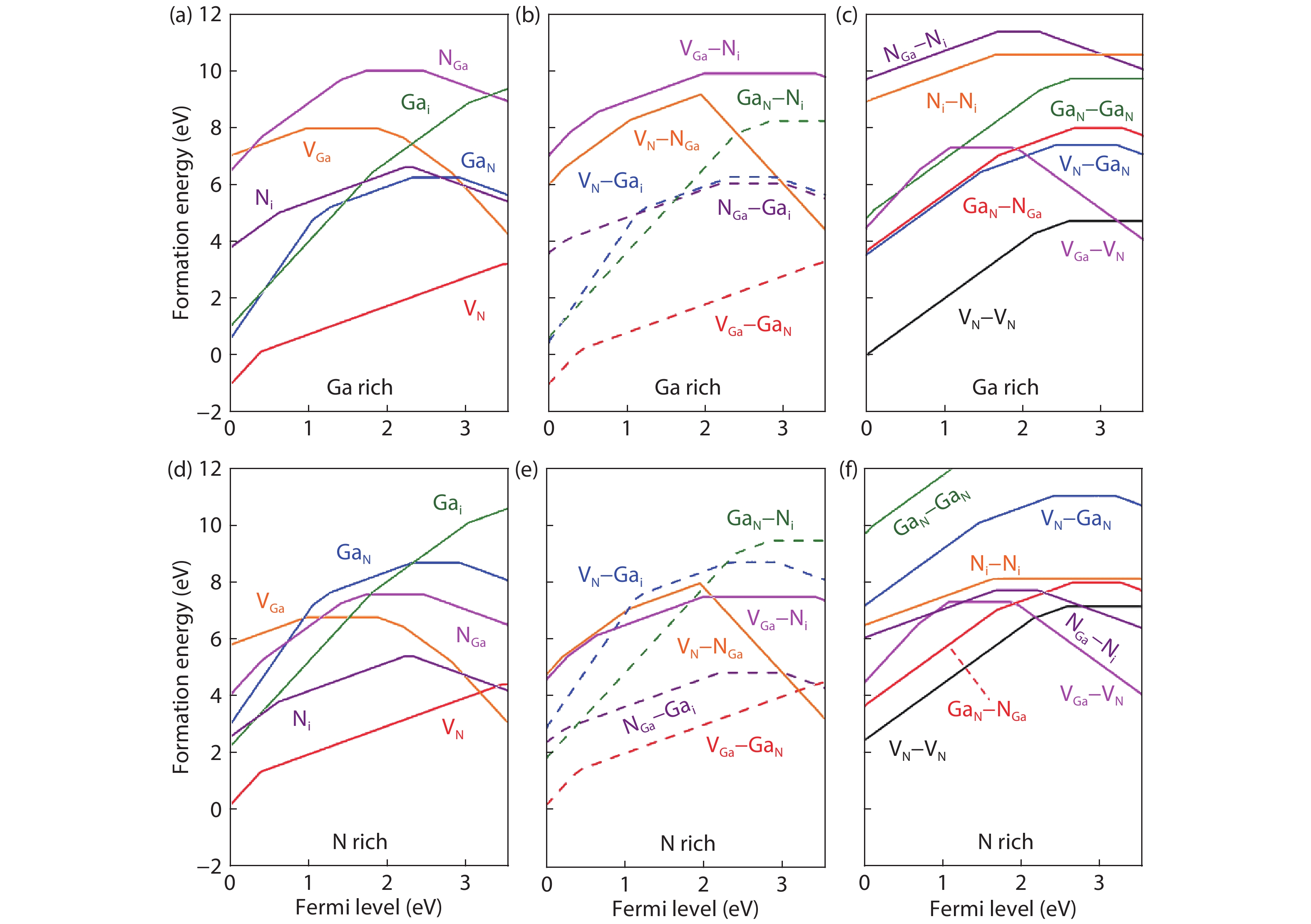
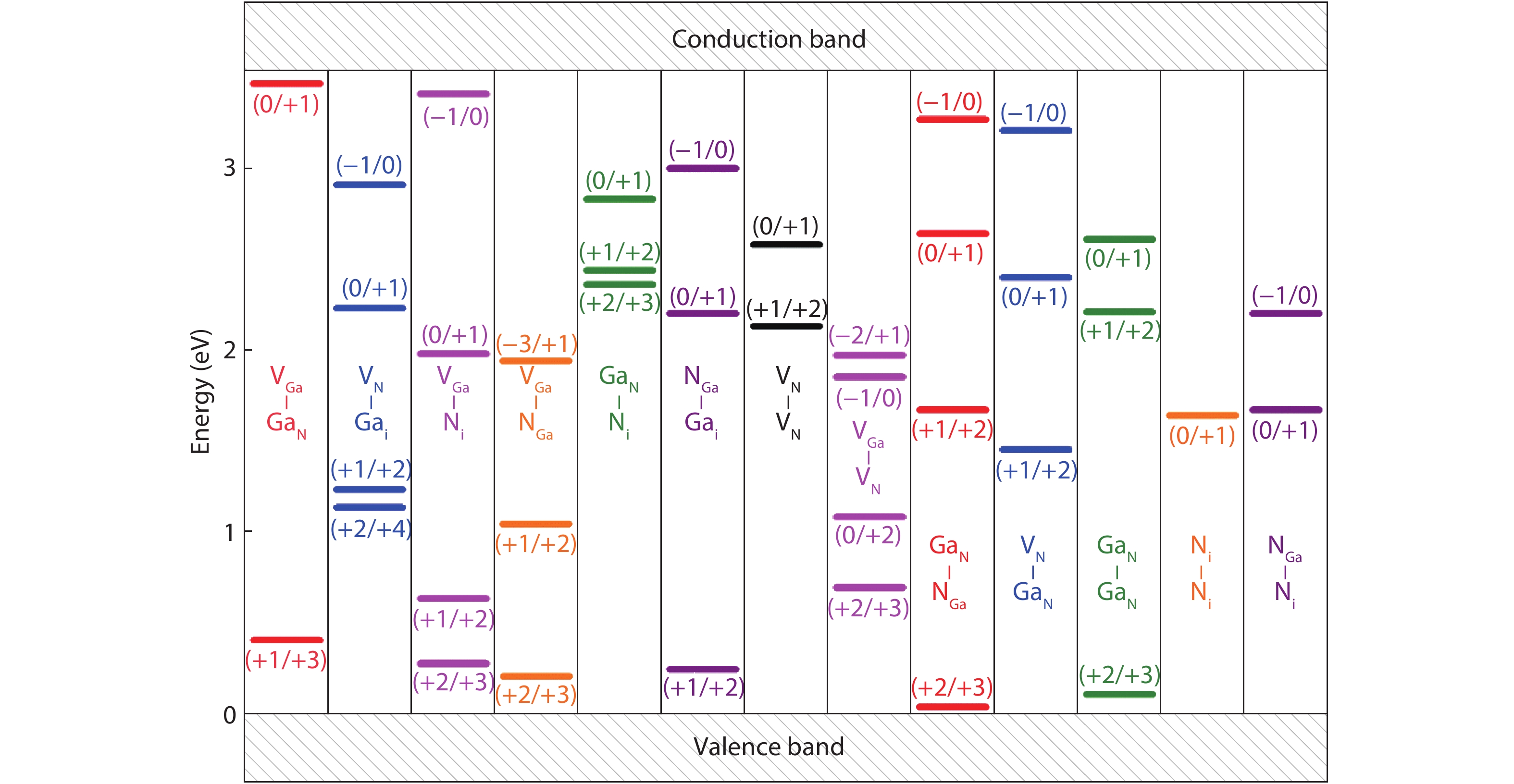
Table 1. The formation energies of two defect-pairs VN–VN and VGa–VN in the neutral state calculated with PBE-relaxed and HSE-relaxed structures (in Ga-rich GaN). 6 structural configurations with different defect-defect distance (in the unrelaxed initial structure) are considered.
| Defect-pair configurations | Initial distance (Å) | Formation energy (eV) PBE-relaxed | Formation energy (eV) HSE-relaxed |
| (VN–VN)-1 | 3.18 | 4.67 | 4.58 |
| (VN–VN)-2 | 3.19 | 4.90 | 4.81 |
| (VN–VN)-3 | 4.51 | 6.83 | 6.39 |
| (VN–VN)-4 | 5.18 | 6.72 | 6.57 |
| (VN–VN)-5 | 5.52 | 6.85 | 6.42 |
| (VN–VN)-6 | 5.53 | 6.85 | 6.41 |
| (VGa–VN)-1 | 1.95 | 7.33 | 7.16 |
| (VGa–VN)-2 | 1.96 | 7.37 | 7.18 |
| (VGa–VN)-3 | 3.23 | 9.37 | 9.06 |
| (VGa–VN)-4 | 3.74 | 9.73 | 8.87 |
| (VGa–VN)-5 | 3.75 | 9.27 | 8.81 |
| (VGa–VN)-6 | 4.54 | 9.37 | 8.89 |
 DownLoad: CSV
Table 2. The calculated formation energies (in eV) of 21 defect-pairs in Ga-rich and N-rich GaN. For each defect-pair, 6 different structural configurations are considered and the distances (in Å) between the two defect sites are listed (before structural relaxation). The lowest-energy configurations are shown in bold. The symbol * means that the defect-pair becomes a point defect or annihilated after structural relaxation.
| Group-1 | |||||||
| Distance | 3.18 | 3.19 | 4.51 | 5.18 | 5.52 | 5.53 | |
| Ga rich | VGa–VGa | 15.81 | 15.84 | 15.96 | 15.89 | 15.89 | 15.87 |
| VGa–NGa | 15.82 | 15.31 | 20.95 | 17.98 | 18.46 | 17.61 | |
| VN–VN | 4.67 | 4.90 | 6.83 | 6.72 | 6.85 | 6.85 | |
| VN–GaN | 7.67 | 7.53 | 8.62 | 8.06 | 8.63 | 8.57 | |
| GaN–GaN | 9.73 | 9.74 | 12.57 | 12.13 | 12.60 | 12.64 | |
| NGa–NGa | 17.40 | 17.49 | 20.32 | 20.11 | 20.17 | 20.26 | |
| N rich | VGa–VGa | 13.37 | 13.40 | 13.53 | 13.45 | 13.45 | 13.43 |
| VGa–NGa | 12.17 | 11.66 | 17.30 | 14.32 | 14.81 | 13.96 | |
| VN–VN | 7.10 | 7.32 | 9.26 | 9.15 | 9.27 | 9.28 | |
| VN–GaN | 11.32 | 11.19 | 12.27 | 11.72 | 12.28 | 12.22 | |
| GaN–GaN | 14.60 | 14.61 | 17.44 | 17.00 | 17.47 | 17.51 | |
| NGa–NGa | 12.53 | 12.62 | 15.45 | 15.24 | 15.30 | 15.39 | |
| Group-2 | |||||||
| Distance | 1.95 | 1.96 | 3.23 | 3.74 | 3.74 | 4.54 | |
| Ga rich | VGa–VN | 7.33 | 7.37 | 9.37 | 9.73 | 9.27 | 9.37 |
| VGa–GaN | 3.28* | 3.26* | 3.30* | 3.28* | 3.26* | 3.30* | |
| VN–NGa | 10.47 | 10.42 | 11.64 | 11.74 | 11.99 | 11.63 | |
| GaN–NGa | 7.99 | 8.62 | 16.50 | 16.35 | 16.02 | 15.42 | |
| N rich | VGa–VN | 7.33 | 7.37 | 9.37 | 9.73 | 9.27 | 9.37 |
| VGa–GaN | 4.50* | 4.47* | 4.52* | 4.50* | 4.47* | 4.52* | |
| VN–NGa | 9.25 | 9.20 | 10.42 | 10.52 | 10.78 | 10.41 | |
| GaN–NGa | 7.99 | 8.62 | 16.50 | 16.35 | 16.02 | 15.42 | |
| Group-3 | |||||||
| Distance | 0.97 | 1.02 | 1.57 | 1.86 | 3.69 | 4.87 | |
| Ga rich | VGa–Gai | 0.00* | 0.00* | 0.00* | 0.00* | 0.00* | 0.00* |
| VGa–Ni | 10.40 | 10.44 | 9.92 | 9.93 | 10.64 | 10.61 | |
| VN–Gai | 6.52* | 6.56* | 6.27* | 6.53* | 11.36 | 11.60 | |
| VN–Ni | 0.00* | 0.00* | 0.00* | 0.00* | 7.66 | 8.42 | |
| GaN–Gai | 11.16 | 11.69 | 12.35 | 11.17 | 12.82 | 14.10 | |
| GaN–Ni | 8.24* | 9.23* | 8.75* | 9.02* | 10.81 | 12.73 | |
| NGa–Gai | 5.98* | 6.10* | 6.29* | 6.26* | 17.41 | 5.98* | |
| NGa–Ni | 11.37 | 15.87 | 13.44 | 11.46 | 11.81 | 15.10 | |
| N rich | VGa–Gai | 0.00* | 0.00* | 0.00* | 0.00* | 0.00* | 0.00* |
| VGa–Ni | 7.97 | 8.00 | 7.48 | 7.50 | 8.21 | 8.18 | |
| VN–Gai | 8.95* | 9.00* | 8.71* | 8.96* | 13.80 | 14.03 | |
| VN–Ni | 0.00* | 0.00* | 0.00* | 0.00* | 7.66 | 8.42 | |
| GaN–Gai | 14.81 | 15.34 | 16.00 | 14.82 | 16.47 | 17.75 | |
| GaN–Ni | 9.45* | 10.45* | 9.97* | 10.24* | 12.03* | 13.95 | |
| NGa–Gai | 4.76* | 4.88* | 5.07* | 5.04* | 16.19 | 4.76* | |
| NGa–Ni | 7.72 | 12.22 | 9.79 | 7.80 | 8.15 | 11.45 | |
| Group-4 | |||||||
| Distance | 1.62 | 1.98 | 2.62 | 2.83 | 3.20 | 3.82 | |
| Ga rich | Gai–Gai | 14.92 | 14.93 | 15.94 | 14.64 | 14.92 | 16.13 |
| Gai–Ni | 14.08 | 13.51 | 13.54 | 14.67 | 14.07 | 27.75 | |
| Ni–Ni | 11.14 | 10.56 | 10.85 | 12.28 | 18.05 | 15.49 | |
| N rich | Gai–Gai | 17.36 | 17.36 | 18.38 | 17.07 | 17.36 | 18.57 |
| Gai–Ni | 14.08 | 13.51 | 13.54 | 14.67 | 14.07 | 27.75 | |
| Ni–Ni | 8.70 | 8.13 | 8.41 | 9.84 | 15.62 | 13.06 | |
DownLoad: CSV
| [1] |
Nakamura S, Mukai T, Senoh M. Candela-class high-brightness InGaN/AlGaN double-heterostructure blue-light-emitting diodes. Appl Phys Lett, 1994, 64(13), 1687 doi: 10.1063/1.111832
|
| [2] |
Kim M H, Schubert M F, Dai Q, et al. Origin of efficiency droop in GaN-based light-emitting diodes. Appl Phys Lett, 2007, 91(18), 183507 doi: 10.1063/1.2800290
|
| [3] |
Pimputkar S, Speck J S, DenBaars S P, et al. Prospects for LED lighting. Nat Photonics, 2009, 3(4), 180 doi: 10.1038/nphoton.2009.32
|
| [4] |
Sheppard S T, Doverspike K, Pribble W L, et al. High-power microwave GaN/AlGaN HEMTs on semi-insulating silicon carbide substrates. IEEE Electron Device Lett, 1999, 20(4), 161 doi: 10.1109/55.753753
|
| [5] |
Pearton S J, Deist R, Ren F, et al. Review of radiation damage in GaN-based materials and devices. J Vac Sci Technol A, 2013, 31(5), 050801 doi: 10.1116/1.4799504
|
| [6] |
Wang J, Mulligan P, Brillson L, et al. Review of using gallium nitride for ionizing radiation detection. Appl Phys Rev, 2015, 2(3), 031102 doi: 10.1063/1.4929913
|
| [7] |
Pearton S J, Ren F, Patrick E, et al. Review-ionizing radiation damage effects on GaN devices. ECS J Solid State Sci Technol, 2015, 5(2), Q35 doi: 10.1149/2.0251602jss
|
| [8] |
Pearton S J, Hwang Y S, Ren F. Radiation effects in GaN-based high electron mobility transistors. J Mater, 2015, 67(7), 1601 doi: 10.1007/s11837-015-1359-y
|
| [9] |
Khanna S M, Estan D, Houdayer A, et al. Proton radiation damage at low temperature in GaAs and GaN light-emitting diodes. IEEE Trans Nucl Sci, 2004, 51(6), 3585 doi: 10.1109/TNS.2004.839105
|
| [10] |
Lorenz K, Peres M, Franco N, et al. Radiation damage formation and annealing in GaN and ZnO. Proc SPIE, 2011
|
| [11] |
Polyakov A Y, Smirnov N B, Govorkov A V, et al. Neutron radiation effects in epitaxially laterally overgrown GaN films. J Electron Mater, 2007, 36(10), 1320 doi: 10.1007/s11664-007-0203-8
|
| [12] |
Pearton S J, Deist R, Polyakov A Y, et al. Radiation damage in GaN-based materials and devicesin. In: Advanced Energy Materials. Hoboken: John Wiley & Sons, Inc., 2014, 345
|
| [13] |
Nord J, Nordlund K, Keinonen J. Molecular dynamics study of damage accumulation in GaN during ion beam irradiation. Phys Rev B, 2003, 68(18), 184104 doi: 10.1103/PhysRevB.68.184104
|
| [14] |
Bryant F J, Webster E. Threshold energy for atomic displacement in cadmium telluride. Phys Status Solidi B, 1967, 21(1), 315 doi: 10.1002/pssb.19670210132
|
| [15] |
Bryant F J, Cox A F J, Frank F C. Experimental and calculated atomic displacement threshold energies for binary semiconductors. Proceedings of the Royal Society of London, Ser A, 1969, 310(1502), 319 doi: 10.1098/rspa.1969.0078
|
| [16] |
Von Bardeleben H J, Cantin J L, Gerstmann U, et al. Identification of the nitrogen split interstitial (N-N)N in GaN. Phys Rev Lett, 2012, 109(20), 206402 doi: 10.1103/PhysRevLett.109.206402
|
| [17] |
Van de Walle C G, Neugebauer J. First-principles calculations for defects and impurities: Applications to III-nitrides. J Appl Phys, 2004, 95(8), 3851 doi: 10.1063/1.1682673
|
| [18] |
Reshchikov M A, Morkoç H. Luminescence properties of defects in GaN. J Appl Phys, 2005, 97(6), 061301 doi: 10.1063/1.1868059
|
| [19] |
Lyons J L, Alkauskas A, Janotti A, et al. First-principles theory of acceptors in nitride semiconductors. Phys Status Solidi B, 2015, 252(5), 900 doi: 10.1002/pssb.201552062
|
| [20] |
Lyons J L, Van de Walle C G. Computationally predicted energies and properties of defects in GaN. npj Comp Mater, 2017, 3(1), 12 doi: 10.1038/s41524-017-0014-2
|
| [21] |
Polyakov A Y, Lee I H. Deep traps in GaN-based structures as affecting the performance of GaN devices. Mater Sci Eng R, 2015, 94, 1 doi: 10.1016/j.mser.2015.05.001
|
| [22] |
Mattila T, Nieminen R M. Point-defect complexes and broadband luminescence in GaN and AlN. Phys Rev B, 1997, 55(15), 9571 doi: 10.1103/PhysRevB.55.9571
|
| [23] |
Diallo I C, Demchenko D O. Native Point defects in GaN: a hybrid-functional study. Phys Rev Appl, 2016, 6(6), 064002 doi: 10.1103/PhysRevApplied.6.064002
|
| [24] |
Li Y G, Yang Y, Short M P, et al. IM3D: A parallel Monte Carlo code for efficient simulations of primary radiation displacements and damage in 3D geometry. Sci Rep, 2015, 5(1), 18130 doi: 10.1038/srep18130
|
| [25] |
Sham L J. Self-consistent equations including exchange and correlation effects. Phys Rev, 1965, 140(4A), A1138 doi: 10.1103/PhysRev.140.A1133
|
| [26] |
Kresse G, Joubert D. From ultrasoft pseudopotentials to the projector augmented-wave method. Phys Rev B, 1999, 59(3), 1758 doi: 10.1103/PhysRevB.59.1758
|
| [27] |
Blöchl P E. Projector augmented-wave method. Phys Rev B, 1994, 50(24), 17953 doi: 10.1103/PhysRevB.50.17953
|
| [28] |
Kresse G, Furthmüller J. Efficient iterative schemes for ab initio total-energy calculations using a plane-wave basis set. Phys Rev B, 1996, 54(16), 11169 doi: 10.1103/PhysRevB.54.11169
|
| [29] |
Perdew J P, Burke K, Ernzerhof M. Generalized gradient approximation made simple. Phys Rev Lett, 1996, 77(18), 3865 doi: 10.1103/PhysRevLett.77.3865
|
| [30] |
Heyd J, Scuseria G E, Ernzerhof M. Erratum: “Hybrid functionals based on a screened Coulomb potential” [J. Chem. Phys. 118, 8207(2003)]. J Chem Phys, 2006, 124(21), 219906 doi: 10.1063/1.2204597
|
| [31] |
Heyd J, Scuseria G E, Ernzerhof M. Hybrid functionals based on a screened Coulomb potential. J Chem Phys, 2003, 118(18), 8207 doi: 10.1063/1.1564060
|
| [32] |
Monemar B. Fundamental energy gap of GaN from photoluminescence excitation spectra. Phys Rev B, 1974, 10(2), 676 doi: 10.1103/PhysRevB.10.676
|
| [33] |
Lany S, Zunger A. Assessment of correction methods for the band-gap problem and for finite-size effects in supercell defect calculations: Case studies for ZnO and GaAs. Phys Rev B, 2008, 78(23), 235104 doi: 10.1103/PhysRevB.78.235104
|
| [34] |
Makov G, Payne M C. Periodic boundary conditions in ab initio calculations. Phys Rev B, 1995, 51(7), 4014 doi: 10.1103/PhysRevB.51.4014
|
| [35] |
Lyons J L, Janotti A, Walle C G. Carbon impurities and the yellow luminescence in GaN. Appl Phys Lett, 2010, 97(15), 152108 doi: 10.1063/1.3492841
|
| [36] |
Freysoldt C, Grabowski B, Hickel T, et al. First-principles calculations for point defects in solids. Rev Mod Phys, 2014, 86(1), 253 doi: 10.1103/RevModPhys.86.253
|


Article views: 5579 Times PDF downloads: 309 Times Cited by: 0 Times
Received: 06 February 2020 Revised: 18 February 2020 Online: Accepted Manuscript: 02 March 2020Uncorrected proof: 02 March 2020Published: 01 March 2020
| Citation: |
He Li, Menglin Huang, Shiyou Chen. First-principles exploration of defect-pairs in GaN[J]. Journal of Semiconductors, 2020, 41(3): 032104. doi: 10.1088/1674-4926/41/3/032104
****
H Li, M L Huang, S Y Chen, First-principles exploration of defect-pairs in GaN[J]. J. Semicond., 2020, 41(3): 032104. doi: 10.1088/1674-4926/41/3/032104.

|
| [1] |
Nakamura S, Mukai T, Senoh M. Candela-class high-brightness InGaN/AlGaN double-heterostructure blue-light-emitting diodes. Appl Phys Lett, 1994, 64(13), 1687 doi: 10.1063/1.111832
|
| [2] |
Kim M H, Schubert M F, Dai Q, et al. Origin of efficiency droop in GaN-based light-emitting diodes. Appl Phys Lett, 2007, 91(18), 183507 doi: 10.1063/1.2800290
|
| [3] |
Pimputkar S, Speck J S, DenBaars S P, et al. Prospects for LED lighting. Nat Photonics, 2009, 3(4), 180 doi: 10.1038/nphoton.2009.32
|
| [4] |
Sheppard S T, Doverspike K, Pribble W L, et al. High-power microwave GaN/AlGaN HEMTs on semi-insulating silicon carbide substrates. IEEE Electron Device Lett, 1999, 20(4), 161 doi: 10.1109/55.753753
|
| [5] |
Pearton S J, Deist R, Ren F, et al. Review of radiation damage in GaN-based materials and devices. J Vac Sci Technol A, 2013, 31(5), 050801 doi: 10.1116/1.4799504
|
| [6] |
Wang J, Mulligan P, Brillson L, et al. Review of using gallium nitride for ionizing radiation detection. Appl Phys Rev, 2015, 2(3), 031102 doi: 10.1063/1.4929913
|
| [7] |
Pearton S J, Ren F, Patrick E, et al. Review-ionizing radiation damage effects on GaN devices. ECS J Solid State Sci Technol, 2015, 5(2), Q35 doi: 10.1149/2.0251602jss
|
| [8] |
Pearton S J, Hwang Y S, Ren F. Radiation effects in GaN-based high electron mobility transistors. J Mater, 2015, 67(7), 1601 doi: 10.1007/s11837-015-1359-y
|
| [9] |
Khanna S M, Estan D, Houdayer A, et al. Proton radiation damage at low temperature in GaAs and GaN light-emitting diodes. IEEE Trans Nucl Sci, 2004, 51(6), 3585 doi: 10.1109/TNS.2004.839105
|
| [10] |
Lorenz K, Peres M, Franco N, et al. Radiation damage formation and annealing in GaN and ZnO. Proc SPIE, 2011
|
| [11] |
Polyakov A Y, Smirnov N B, Govorkov A V, et al. Neutron radiation effects in epitaxially laterally overgrown GaN films. J Electron Mater, 2007, 36(10), 1320 doi: 10.1007/s11664-007-0203-8
|
| [12] |
Pearton S J, Deist R, Polyakov A Y, et al. Radiation damage in GaN-based materials and devicesin. In: Advanced Energy Materials. Hoboken: John Wiley & Sons, Inc., 2014, 345
|
| [13] |
Nord J, Nordlund K, Keinonen J. Molecular dynamics study of damage accumulation in GaN during ion beam irradiation. Phys Rev B, 2003, 68(18), 184104 doi: 10.1103/PhysRevB.68.184104
|
| [14] |
Bryant F J, Webster E. Threshold energy for atomic displacement in cadmium telluride. Phys Status Solidi B, 1967, 21(1), 315 doi: 10.1002/pssb.19670210132
|
| [15] |
Bryant F J, Cox A F J, Frank F C. Experimental and calculated atomic displacement threshold energies for binary semiconductors. Proceedings of the Royal Society of London, Ser A, 1969, 310(1502), 319 doi: 10.1098/rspa.1969.0078
|
| [16] |
Von Bardeleben H J, Cantin J L, Gerstmann U, et al. Identification of the nitrogen split interstitial (N-N)N in GaN. Phys Rev Lett, 2012, 109(20), 206402 doi: 10.1103/PhysRevLett.109.206402
|
| [17] |
Van de Walle C G, Neugebauer J. First-principles calculations for defects and impurities: Applications to III-nitrides. J Appl Phys, 2004, 95(8), 3851 doi: 10.1063/1.1682673
|
| [18] |
Reshchikov M A, Morkoç H. Luminescence properties of defects in GaN. J Appl Phys, 2005, 97(6), 061301 doi: 10.1063/1.1868059
|
| [19] |
Lyons J L, Alkauskas A, Janotti A, et al. First-principles theory of acceptors in nitride semiconductors. Phys Status Solidi B, 2015, 252(5), 900 doi: 10.1002/pssb.201552062
|
| [20] |
Lyons J L, Van de Walle C G. Computationally predicted energies and properties of defects in GaN. npj Comp Mater, 2017, 3(1), 12 doi: 10.1038/s41524-017-0014-2
|
| [21] |
Polyakov A Y, Lee I H. Deep traps in GaN-based structures as affecting the performance of GaN devices. Mater Sci Eng R, 2015, 94, 1 doi: 10.1016/j.mser.2015.05.001
|
| [22] |
Mattila T, Nieminen R M. Point-defect complexes and broadband luminescence in GaN and AlN. Phys Rev B, 1997, 55(15), 9571 doi: 10.1103/PhysRevB.55.9571
|
| [23] |
Diallo I C, Demchenko D O. Native Point defects in GaN: a hybrid-functional study. Phys Rev Appl, 2016, 6(6), 064002 doi: 10.1103/PhysRevApplied.6.064002
|
| [24] |
Li Y G, Yang Y, Short M P, et al. IM3D: A parallel Monte Carlo code for efficient simulations of primary radiation displacements and damage in 3D geometry. Sci Rep, 2015, 5(1), 18130 doi: 10.1038/srep18130
|
| [25] |
Sham L J. Self-consistent equations including exchange and correlation effects. Phys Rev, 1965, 140(4A), A1138 doi: 10.1103/PhysRev.140.A1133
|
| [26] |
Kresse G, Joubert D. From ultrasoft pseudopotentials to the projector augmented-wave method. Phys Rev B, 1999, 59(3), 1758 doi: 10.1103/PhysRevB.59.1758
|
| [27] |
Blöchl P E. Projector augmented-wave method. Phys Rev B, 1994, 50(24), 17953 doi: 10.1103/PhysRevB.50.17953
|
| [28] |
Kresse G, Furthmüller J. Efficient iterative schemes for ab initio total-energy calculations using a plane-wave basis set. Phys Rev B, 1996, 54(16), 11169 doi: 10.1103/PhysRevB.54.11169
|
| [29] |
Perdew J P, Burke K, Ernzerhof M. Generalized gradient approximation made simple. Phys Rev Lett, 1996, 77(18), 3865 doi: 10.1103/PhysRevLett.77.3865
|
| [30] |
Heyd J, Scuseria G E, Ernzerhof M. Erratum: “Hybrid functionals based on a screened Coulomb potential” [J. Chem. Phys. 118, 8207(2003)]. J Chem Phys, 2006, 124(21), 219906 doi: 10.1063/1.2204597
|
| [31] |
Heyd J, Scuseria G E, Ernzerhof M. Hybrid functionals based on a screened Coulomb potential. J Chem Phys, 2003, 118(18), 8207 doi: 10.1063/1.1564060
|
| [32] |
Monemar B. Fundamental energy gap of GaN from photoluminescence excitation spectra. Phys Rev B, 1974, 10(2), 676 doi: 10.1103/PhysRevB.10.676
|
| [33] |
Lany S, Zunger A. Assessment of correction methods for the band-gap problem and for finite-size effects in supercell defect calculations: Case studies for ZnO and GaAs. Phys Rev B, 2008, 78(23), 235104 doi: 10.1103/PhysRevB.78.235104
|
| [34] |
Makov G, Payne M C. Periodic boundary conditions in ab initio calculations. Phys Rev B, 1995, 51(7), 4014 doi: 10.1103/PhysRevB.51.4014
|
| [35] |
Lyons J L, Janotti A, Walle C G. Carbon impurities and the yellow luminescence in GaN. Appl Phys Lett, 2010, 97(15), 152108 doi: 10.1063/1.3492841
|
| [36] |
Freysoldt C, Grabowski B, Hickel T, et al. First-principles calculations for point defects in solids. Rev Mod Phys, 2014, 86(1), 253 doi: 10.1103/RevModPhys.86.253
|

 WeChat ID
Journal of Semiconductors © 2017 All Rights Reserved 京ICP备05085259号-2


