


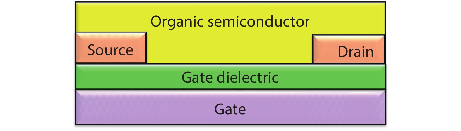
Fig. 1.
(Color online) Schematic representation of the bottom gate bottom contact organic thin film transistor.
ARTICLES
Corresponding author: Brijesh Kumar, bkiitr@gmail.com
Abstract: Steady state behavior analysis of organic thin film transistor (OTFTs) has been thoroughly researched in the past few decades. Yet, this static logic analysis has drawbacks of high power dissipation and high power consumption, and a large number of prerequisites in the number of transistors for the digital logic circuit application. Hence, to overcome these basic fundamental drawbacks of static logic, the dynamic logic study of organic thin film transistor has been analyzed in this paper. The fundamental basic of dynamic logic is a pass transistor for which logic high and logic low model is designed at an operating voltage of 5 V and frequency of 5 kHz. Additionally, the novel approach of analytical model for organic pass transistor (OPT) circuit is included and verified using MATLAB. The transient individualities of organic pass transistor OPT are examined through Atlas 2-D numerical device simulator. The reduction in the power dissipation along with additional voltage scaling and reduction in the clock frequency such as pipelining may further enable the applications into more complex VLSI ICs.
Keywords: organic-pass transistor (OPT), logic high, logic low, pseudo-p, dynamic state, analytical model
| [1] |
Klauk H. Organic electronics: materials, manufacturing, and applications. Weinheim: John Wiley & Sons, 2006
|
| [2] |
Kumar B, Kaushik B K, Negi Y S, et al. Perspectives and challenges for organic thin film transistors: Materials, devices, processes and applications. J Mater Sci: Mater Electron, 2014, 25(1), 1 doi: 10.1007/s10854-013-1550-2
|
| [3] |
Kumar B, Kaushik B K, Negi Y S, et al. Organic thin film transistors characteristics parameters, structures and their applications. Recent Advances in Intelligent Computational Systems (RAICS), 2011, 706
|
| [4] |
Kumar B, Kaushik B K, Negi Y S, et al. Organic thin film transistors: Structures, models, materials, fabrication, and applications: A review. Polym Rev, 2014, 54(1), 33 doi: 10.1080/15583724.2013.848455
|
| [5] |
Bode D, Rolin C, Schols S, et al. Noise-margin analysis for organic thin-film complementary technology. IEEE Trans Electron Devices, 2010, 57(1), 201 doi: 10.1109/TED.2009.2035546
|
| [6] |
Kumar B, Kaushik B K, Negi Y S, et al. Static and dynamic analysis of organic and hybrid inverter circuits. J Comput Electron, 2013, 12(4), 765 doi: 10.1007/s10825-013-0476-5
|
| [7] |
Huang T C, Fukuda K, Lo C M, et al. Pseudo-CMOS: A design style for low-cost and robust flexible electronics. IEEE Trans Electron Devices, 2011, 58(1), 141 doi: 10.1109/TED.2010.2088127
|
| [8] |
Kimura M, Sawamoto D, Matsuda T, et al. Pseudo-CMOS circuits using amorphous In–Sn–Zn–O thin-film transistors. Dig Tech Pap - SID Int Symp, 2014, 45(1), 960 doi: 10.1002/j.2168-0159.2014.tb00249.x
|
| [9] |
Kumar B, Kaushik B K, Negi Y S, et al. Single and dual gate OTFT based robust organic digital design. Microelectron Reliab, 2014, 54(1), 100 doi: 10.1016/j.microrel.2013.09.015
|
| [10] |
Venturelli M, Torricelli F, Ghittorelli M, et al. Unipolar differential logic for large-scale integration of flexible a-IGZO circuits. IEEE Trans Circuits Syst II, 2017, 64(5), 565 doi: 10.1109/TCSII.2016.2578951
|
| [11] |
Myny K. The development of flexible integrated circuits based on thin-film transistors. Nat Electron, 2018, 1(1), 30 doi: 10.1038/s41928-017-0008-6
|
| [12] |
Kim J S, Jang J H, Kim Y D, et al. Dynamic logic circuits using a-IGZO TFTs. IEEE Trans Electron Devices, 2017, 64(10), 4123 doi: 10.1109/TED.2017.2738665
|
| [13] |
Elsobky M, Elattar M, Alavi G, et al. A digital library for a flexible low-voltage organic thin-film transistor technology. Org Electron Phys Mater Appl, 2017, 50, 491 doi: 10.1016/j.orgel.2017.08.028
|
| [14] |
Leblebici Y, Kang S M. CMOS digital integrated circuits: analysis and design. McGraw-Hill, 1996
|
| [15] |
Kumar B, Kaushik B K, Negi Y S, et al. Modeling of top and bottom contact structure organic field effect transistors. J Vac Sci Technol B, 2013, 31(1), 012401 doi: 10.1116/1.4773054
|
| [16] |
Kumar B, Kaushik B K, Negi Y S, et al. Analytical modeling and parameter extraction of top and bottom contact structures of organic thin film transistors. Microelectron J, 2013, 44(9), 736 doi: 10.1016/j.mejo.2013.06.004
|
| [17] |
IEEE standard test methods for the characterization of organic transistors and materials. IEEE Std, 2004, 1620
|
| [18] |
Mittal P, Kumar B, Negi Y S, et al. Channel length variation effect on performance parameters of organic field effect transistors. Microelectronics J, 2012, 43, 985 doi: 10.1016/j.mejo.2012.07.016
|
| [19] |
Marinov O, Deen M J, Zschieschang U, et al. Organic thin-film transistors: Part I—Compact DC modelling. IEEE Trans Electron Devices, 2009, 56(12), 2952 doi: 10.1109/TED.2009.2033308
|
| [20] |
Gundlach D J, Zhou L, Nichols J A, et al. An experimental study of contact effects in organic thin film transistors. J Appl Phys, 2006, 100, 024509 doi: 10.1063/1.2215132
|
| [21] |
Hamilton M C, Martin S, Kanicki J. Field-effect mobility of organic polymer thin-film transistors. Chem Mater, 2004, 16, 4699 doi: 10.1021/cm049613r
|
| [22] |
Gupta D, Katiyar M, Gupta D, et al. Mobility estimation incorporating the effects of contact resistance and gate voltage dependent mobility in top contact organic thin film transistors. Proc of ASID, 2006, 6
|
| [23] |
ATLAS user’s manual. Silvaco International, Santa Clara, CA, USA, www.silvaco.com, 2014
|
| [24] |
Mittal P, Negi Y S, Singh R K. Impact of source and drain contact thickness on the performance of organic thin film transistors. J Semicond, 2014, 35(12), 124002 doi: 10.1088/1674-4926/35/12/124002
|
| [25] |
Baker R J. CMOS: circuit design, layout, and simulation. New Jersey: Wiley, 2011
|
| [26] |
Escoffier R, Fichtner W, Fokkema D, et al. DESSIS 10.0 manual. ISE Integr Syst Eng AG: CH-Zürich, 1996, 96, 161
|
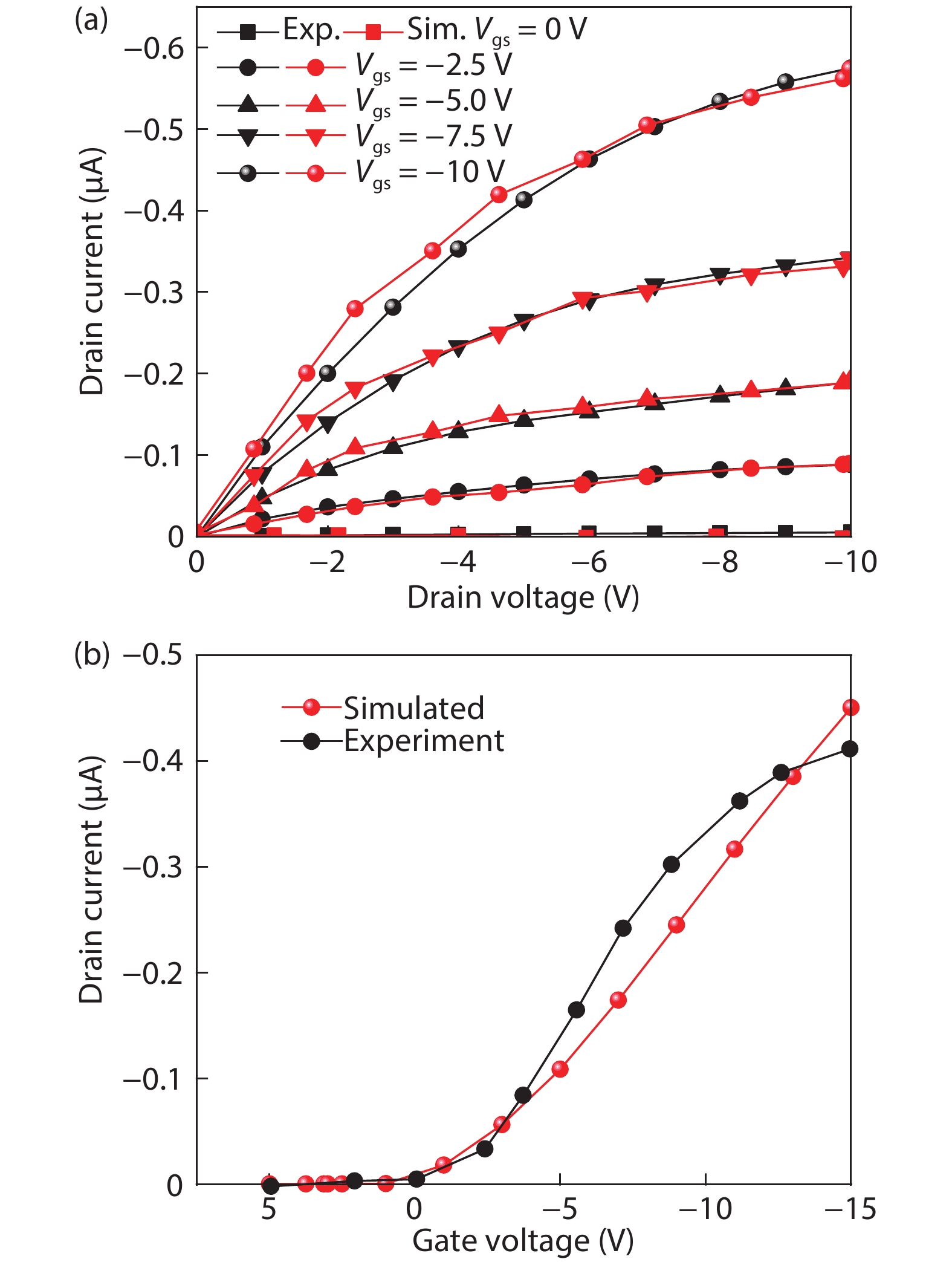
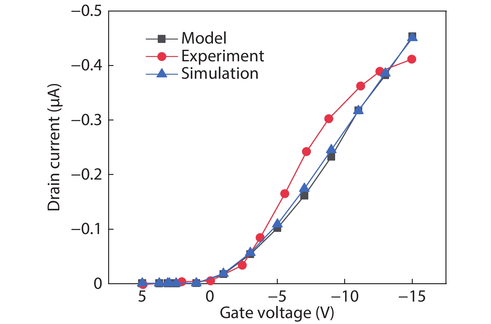
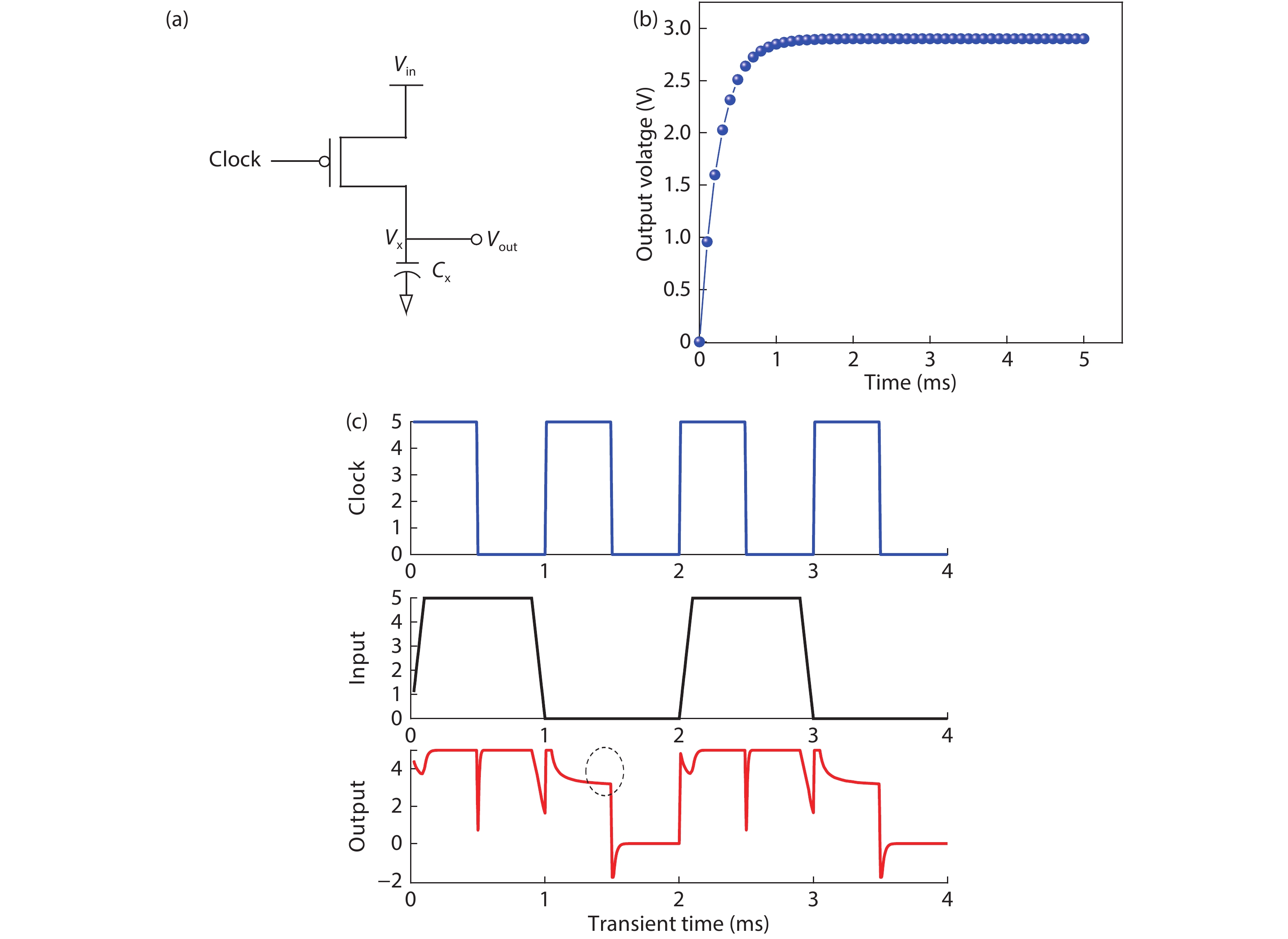
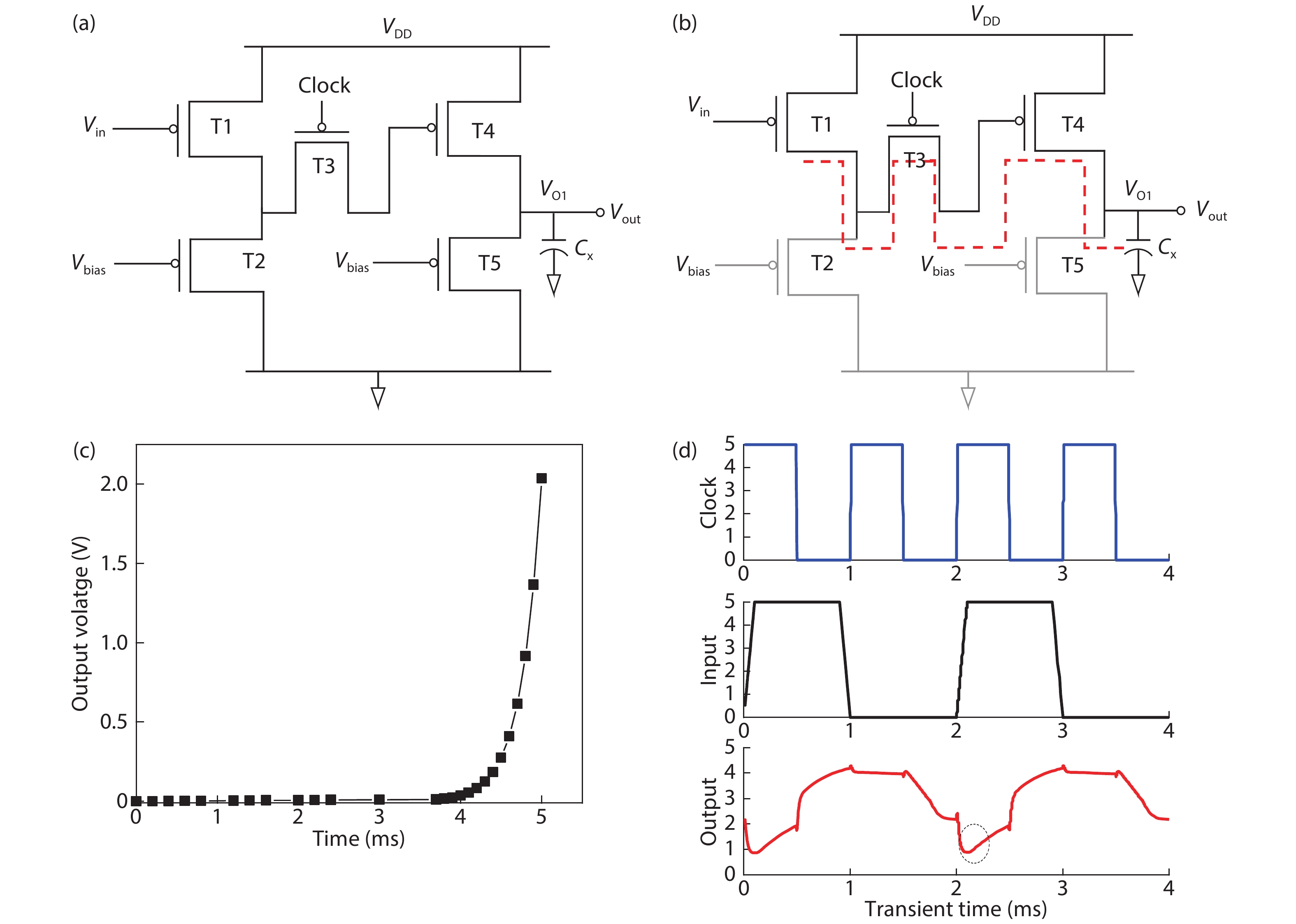
Table 1. Device parameters for the organic material based device[9].
| Parameter | Value |
| Gate electrode (Si) | 150 nm |
| Bottom gate (SiO2), tox | 100 nm |
| OSC thickness (tosc) (pentacene) | 200 nm |
| Width of S/D (ts/td) (gold) | 80 nm |
| Active layer length (L) | 25 µm |
| Active layer width (W) | 800 µm |
 DownLoad: CSV
Table 2. Electrical parameter comparison of pentacene-based single gate organic thin film transistor.
| Parameter | Experiment[9] | Simulated |
| µ (cm2/(V·s)) | 0.02 | 0.019 |
| Ion/Ioff | 3.2 × 10³ | 5.1 × 10³ |
| SS (V/dec.) | 2.0 | 2.3 |
| gm (µS) | 0.044 | 0.041 |
| VTH (V) | – 2.0 | – 2.1 |
DownLoad: CSV
Table 3. Fitting parameters for the transfer characteristics using the model through MATLAB[21].
DownLoad: CSV
Table 4. Comparison between analytical and simulation parameters for logic high transfer signal.
| Parameter | Analytical | Simulated |
| Output voltage (V) | 2.89 | 3 |
DownLoad: CSV
Table 5. Dimensions for the simulated parameters of the proposed inverter design.
| Parameter | Value |
| W/L (T1) | 5000 μm/100 μm |
| W/L (T2) | 300 μm/100 μm |
| W/L (T3) | 300 μm/100 μm |
| W/L (T4) | 5000 μm/100 μm |
| W/L (T5) | 300 μm/100 μm |
| COLED | 0.6 nF |
DownLoad: CSV
Table 6. Comparison between analytical and simulation parameters for logic low transfer signal.
| Parameter | Analytical | Simulated |
| Output voltage (V) | 0.012 | 0.5 |
DownLoad: CSV
| [1] |
Klauk H. Organic electronics: materials, manufacturing, and applications. Weinheim: John Wiley & Sons, 2006
|
| [2] |
Kumar B, Kaushik B K, Negi Y S, et al. Perspectives and challenges for organic thin film transistors: Materials, devices, processes and applications. J Mater Sci: Mater Electron, 2014, 25(1), 1 doi: 10.1007/s10854-013-1550-2
|
| [3] |
Kumar B, Kaushik B K, Negi Y S, et al. Organic thin film transistors characteristics parameters, structures and their applications. Recent Advances in Intelligent Computational Systems (RAICS), 2011, 706
|
| [4] |
Kumar B, Kaushik B K, Negi Y S, et al. Organic thin film transistors: Structures, models, materials, fabrication, and applications: A review. Polym Rev, 2014, 54(1), 33 doi: 10.1080/15583724.2013.848455
|
| [5] |
Bode D, Rolin C, Schols S, et al. Noise-margin analysis for organic thin-film complementary technology. IEEE Trans Electron Devices, 2010, 57(1), 201 doi: 10.1109/TED.2009.2035546
|
| [6] |
Kumar B, Kaushik B K, Negi Y S, et al. Static and dynamic analysis of organic and hybrid inverter circuits. J Comput Electron, 2013, 12(4), 765 doi: 10.1007/s10825-013-0476-5
|
| [7] |
Huang T C, Fukuda K, Lo C M, et al. Pseudo-CMOS: A design style for low-cost and robust flexible electronics. IEEE Trans Electron Devices, 2011, 58(1), 141 doi: 10.1109/TED.2010.2088127
|
| [8] |
Kimura M, Sawamoto D, Matsuda T, et al. Pseudo-CMOS circuits using amorphous In–Sn–Zn–O thin-film transistors. Dig Tech Pap - SID Int Symp, 2014, 45(1), 960 doi: 10.1002/j.2168-0159.2014.tb00249.x
|
| [9] |
Kumar B, Kaushik B K, Negi Y S, et al. Single and dual gate OTFT based robust organic digital design. Microelectron Reliab, 2014, 54(1), 100 doi: 10.1016/j.microrel.2013.09.015
|
| [10] |
Venturelli M, Torricelli F, Ghittorelli M, et al. Unipolar differential logic for large-scale integration of flexible a-IGZO circuits. IEEE Trans Circuits Syst II, 2017, 64(5), 565 doi: 10.1109/TCSII.2016.2578951
|
| [11] |
Myny K. The development of flexible integrated circuits based on thin-film transistors. Nat Electron, 2018, 1(1), 30 doi: 10.1038/s41928-017-0008-6
|
| [12] |
Kim J S, Jang J H, Kim Y D, et al. Dynamic logic circuits using a-IGZO TFTs. IEEE Trans Electron Devices, 2017, 64(10), 4123 doi: 10.1109/TED.2017.2738665
|
| [13] |
Elsobky M, Elattar M, Alavi G, et al. A digital library for a flexible low-voltage organic thin-film transistor technology. Org Electron Phys Mater Appl, 2017, 50, 491 doi: 10.1016/j.orgel.2017.08.028
|
| [14] |
Leblebici Y, Kang S M. CMOS digital integrated circuits: analysis and design. McGraw-Hill, 1996
|
| [15] |
Kumar B, Kaushik B K, Negi Y S, et al. Modeling of top and bottom contact structure organic field effect transistors. J Vac Sci Technol B, 2013, 31(1), 012401 doi: 10.1116/1.4773054
|
| [16] |
Kumar B, Kaushik B K, Negi Y S, et al. Analytical modeling and parameter extraction of top and bottom contact structures of organic thin film transistors. Microelectron J, 2013, 44(9), 736 doi: 10.1016/j.mejo.2013.06.004
|
| [17] |
IEEE standard test methods for the characterization of organic transistors and materials. IEEE Std, 2004, 1620
|
| [18] |
Mittal P, Kumar B, Negi Y S, et al. Channel length variation effect on performance parameters of organic field effect transistors. Microelectronics J, 2012, 43, 985 doi: 10.1016/j.mejo.2012.07.016
|
| [19] |
Marinov O, Deen M J, Zschieschang U, et al. Organic thin-film transistors: Part I—Compact DC modelling. IEEE Trans Electron Devices, 2009, 56(12), 2952 doi: 10.1109/TED.2009.2033308
|
| [20] |
Gundlach D J, Zhou L, Nichols J A, et al. An experimental study of contact effects in organic thin film transistors. J Appl Phys, 2006, 100, 024509 doi: 10.1063/1.2215132
|
| [21] |
Hamilton M C, Martin S, Kanicki J. Field-effect mobility of organic polymer thin-film transistors. Chem Mater, 2004, 16, 4699 doi: 10.1021/cm049613r
|
| [22] |
Gupta D, Katiyar M, Gupta D, et al. Mobility estimation incorporating the effects of contact resistance and gate voltage dependent mobility in top contact organic thin film transistors. Proc of ASID, 2006, 6
|
| [23] |
ATLAS user’s manual. Silvaco International, Santa Clara, CA, USA, www.silvaco.com, 2014
|
| [24] |
Mittal P, Negi Y S, Singh R K. Impact of source and drain contact thickness on the performance of organic thin film transistors. J Semicond, 2014, 35(12), 124002 doi: 10.1088/1674-4926/35/12/124002
|
| [25] |
Baker R J. CMOS: circuit design, layout, and simulation. New Jersey: Wiley, 2011
|
| [26] |
Escoffier R, Fichtner W, Fokkema D, et al. DESSIS 10.0 manual. ISE Integr Syst Eng AG: CH-Zürich, 1996, 96, 161
|


Article views: 4642 Times PDF downloads: 46 Times Cited by: 0 Times
Received: 14 November 2019 Revised: 22 January 2020 Online: Accepted Manuscript: 10 April 2020Uncorrected proof: 13 April 2020Published: 01 June 2020
| Citation: |
Shagun Pal, Brijesh Kumar. Mathematical analysis of organic-pass transistor using pseudo-p-OTFTs[J]. Journal of Semiconductors, 2020, 41(6): 062601. doi: 10.1088/1674-4926/41/6/062601
****
S Pal, B Kumar, Mathematical analysis of organic-pass transistor using pseudo-p-OTFTs[J]. J. Semicond., 2020, 41(6): 062601. doi: 10.1088/1674-4926/41/6/062601.

|
| [1] |
Klauk H. Organic electronics: materials, manufacturing, and applications. Weinheim: John Wiley & Sons, 2006
|
| [2] |
Kumar B, Kaushik B K, Negi Y S, et al. Perspectives and challenges for organic thin film transistors: Materials, devices, processes and applications. J Mater Sci: Mater Electron, 2014, 25(1), 1 doi: 10.1007/s10854-013-1550-2
|
| [3] |
Kumar B, Kaushik B K, Negi Y S, et al. Organic thin film transistors characteristics parameters, structures and their applications. Recent Advances in Intelligent Computational Systems (RAICS), 2011, 706
|
| [4] |
Kumar B, Kaushik B K, Negi Y S, et al. Organic thin film transistors: Structures, models, materials, fabrication, and applications: A review. Polym Rev, 2014, 54(1), 33 doi: 10.1080/15583724.2013.848455
|
| [5] |
Bode D, Rolin C, Schols S, et al. Noise-margin analysis for organic thin-film complementary technology. IEEE Trans Electron Devices, 2010, 57(1), 201 doi: 10.1109/TED.2009.2035546
|
| [6] |
Kumar B, Kaushik B K, Negi Y S, et al. Static and dynamic analysis of organic and hybrid inverter circuits. J Comput Electron, 2013, 12(4), 765 doi: 10.1007/s10825-013-0476-5
|
| [7] |
Huang T C, Fukuda K, Lo C M, et al. Pseudo-CMOS: A design style for low-cost and robust flexible electronics. IEEE Trans Electron Devices, 2011, 58(1), 141 doi: 10.1109/TED.2010.2088127
|
| [8] |
Kimura M, Sawamoto D, Matsuda T, et al. Pseudo-CMOS circuits using amorphous In–Sn–Zn–O thin-film transistors. Dig Tech Pap - SID Int Symp, 2014, 45(1), 960 doi: 10.1002/j.2168-0159.2014.tb00249.x
|
| [9] |
Kumar B, Kaushik B K, Negi Y S, et al. Single and dual gate OTFT based robust organic digital design. Microelectron Reliab, 2014, 54(1), 100 doi: 10.1016/j.microrel.2013.09.015
|
| [10] |
Venturelli M, Torricelli F, Ghittorelli M, et al. Unipolar differential logic for large-scale integration of flexible a-IGZO circuits. IEEE Trans Circuits Syst II, 2017, 64(5), 565 doi: 10.1109/TCSII.2016.2578951
|
| [11] |
Myny K. The development of flexible integrated circuits based on thin-film transistors. Nat Electron, 2018, 1(1), 30 doi: 10.1038/s41928-017-0008-6
|
| [12] |
Kim J S, Jang J H, Kim Y D, et al. Dynamic logic circuits using a-IGZO TFTs. IEEE Trans Electron Devices, 2017, 64(10), 4123 doi: 10.1109/TED.2017.2738665
|
| [13] |
Elsobky M, Elattar M, Alavi G, et al. A digital library for a flexible low-voltage organic thin-film transistor technology. Org Electron Phys Mater Appl, 2017, 50, 491 doi: 10.1016/j.orgel.2017.08.028
|
| [14] |
Leblebici Y, Kang S M. CMOS digital integrated circuits: analysis and design. McGraw-Hill, 1996
|
| [15] |
Kumar B, Kaushik B K, Negi Y S, et al. Modeling of top and bottom contact structure organic field effect transistors. J Vac Sci Technol B, 2013, 31(1), 012401 doi: 10.1116/1.4773054
|
| [16] |
Kumar B, Kaushik B K, Negi Y S, et al. Analytical modeling and parameter extraction of top and bottom contact structures of organic thin film transistors. Microelectron J, 2013, 44(9), 736 doi: 10.1016/j.mejo.2013.06.004
|
| [17] |
IEEE standard test methods for the characterization of organic transistors and materials. IEEE Std, 2004, 1620
|
| [18] |
Mittal P, Kumar B, Negi Y S, et al. Channel length variation effect on performance parameters of organic field effect transistors. Microelectronics J, 2012, 43, 985 doi: 10.1016/j.mejo.2012.07.016
|
| [19] |
Marinov O, Deen M J, Zschieschang U, et al. Organic thin-film transistors: Part I—Compact DC modelling. IEEE Trans Electron Devices, 2009, 56(12), 2952 doi: 10.1109/TED.2009.2033308
|
| [20] |
Gundlach D J, Zhou L, Nichols J A, et al. An experimental study of contact effects in organic thin film transistors. J Appl Phys, 2006, 100, 024509 doi: 10.1063/1.2215132
|
| [21] |
Hamilton M C, Martin S, Kanicki J. Field-effect mobility of organic polymer thin-film transistors. Chem Mater, 2004, 16, 4699 doi: 10.1021/cm049613r
|
| [22] |
Gupta D, Katiyar M, Gupta D, et al. Mobility estimation incorporating the effects of contact resistance and gate voltage dependent mobility in top contact organic thin film transistors. Proc of ASID, 2006, 6
|
| [23] |
ATLAS user’s manual. Silvaco International, Santa Clara, CA, USA, www.silvaco.com, 2014
|
| [24] |
Mittal P, Negi Y S, Singh R K. Impact of source and drain contact thickness on the performance of organic thin film transistors. J Semicond, 2014, 35(12), 124002 doi: 10.1088/1674-4926/35/12/124002
|
| [25] |
Baker R J. CMOS: circuit design, layout, and simulation. New Jersey: Wiley, 2011
|
| [26] |
Escoffier R, Fichtner W, Fokkema D, et al. DESSIS 10.0 manual. ISE Integr Syst Eng AG: CH-Zürich, 1996, 96, 161
|

 WeChat ID
Journal of Semiconductors © 2017 All Rights Reserved 京ICP备05085259号-2


