J. Semicond. > 2021, Volume 42 > Issue 2 > 024103

ARTICLES

Integration of GaN analog building blocks on p-GaN wafers for GaN ICs

Xiangdong Li1, 2, , Karen Geens1, Nooshin Amirifar1, Ming Zhao1, Shuzhen You1, Niels Posthuma1, Hu Liang1, Guido Groeseneken1, 2 and Stefaan Decoutere1

+ Author Affiliations

 Corresponding author: Xiangdong Li, lixiangdong28@126.com

DOI: 10.1088/1674-4926/42/2/024103

PDF

Turn off MathJax

Abstract: We demonstrate the key module of comparators in GaN ICs, based on resistor-transistor logic (RTL) on E-mode wafers in this work. The fundamental inverters in the comparator consist of a p-GaN gate HEMT and a 2DEG resistor as the load. The function of the RTL comparators is finally verified by a undervoltage lockout (UVLO) circuit. The compatibility of this circuit with the current p-GaN technology paves the way for integrating logic ICs together with the power devices.

Key words: p-GaNresistor-transistor logic (RTL)comparatorundervoltage lockout (UVLO)GaN ICs


[1]
Dan K. GaN power IC technology: Past, present, and future. 2017 29th International Symposium on Power Semiconductor Devices and IC's (ISPSD), 2017, 19
[2]
Uemoto Y, Morita T, Ikoshi A, et al. GaN monolithic inverter IC using normally-off gate injection transistors with planar isolation on Si substrate. 2009 IEEE International Electron Devices Meeting (IEDM), 2009, 1
[3]
Moench S, Kallfass I, Reiner R, et al. Single-input GaN gate driver based on depletion-mode logic integrated with a 600 V GaN-on-Si power transistor. 2016 IEEE 4th Work Wide Bandgap Power Devices Appl Wipda, 2016, 204
[4]
Tang G, Kwan M H, Zhang Z, et al. High-speed, high-reliability GaN power device with integrated gate driver. Proc ISPSD, 2018, 76
[5]
Li X D, van Hove M, Zhao M, et al. 200 V enhancement-mode p-GaN HEMTs fabricated on 200 mm GaN-on-SOI with trench isolation for monolithic integration. IEEE Electron Device Lett, 2017, 38, 918 doi: 10.1109/LED.2017.2703304
[6]
Li X D, van Hove M, Zhao M, et al. Suppression of the backgating effect of enhancement-mode p-GaN HEMTs on 200-mm GaN-on-SOI for monolithic integration. IEEE Electron Device Lett, 2018, 39, 999 doi: 10.1109/LED.2018.2833883
[7]
Li X D, Geens K, Guo W M, et al. Demonstration of GaN integrated half-bridge with on-chip drivers on 200-mm engineered substrates. IEEE Electron Device Lett, 2019, 40, 1499 doi: 10.1109/LED.2019.2929417
[8]
Li X, Amirifar N, Geens K, et al. GaN-on-SOI: Monolithically integrated all-GaN ICs for power conversion. 2019 IEEE International Electron Devices Meeting (IEDM), 2019, 4.4.1
[9]
Li X D, van Hove M, Zhao M, et al. Investigation on carrier transport through AlN nucleation layer from differently doped Si(111) substrates. IEEE Trans Electron Devices, 2018, 65, 1721 doi: 10.1109/TED.2018.2810886
[10]
Li X D, Zhao M, Bakeroot B, et al. Buffer vertical leakage mechanism and reliability of 200-mm GaN-on-SOI. IEEE Trans Electron Devices, 2019, 66, 553 doi: 10.1109/TED.2018.2878457
[11]
Geens K, Li X D, Zhao M, et al. 650 V p-GaN gate power HEMTs on 200 mm engineered substrates. 2019 IEEE 7th Workshop on Wide Bandgap Power Devices and Applications (WiPDA), 2019, 292
[12]
Liu X S, Chen K J. GaN single-polarity power supply bootstrapped comparator for high-temperature electronics. IEEE Electron Device Lett, 2011, 32, 27 doi: 10.1109/LED.2010.2088376
[13]
van Hove M, Boulay S, Bahl S R, et al. CMOS process-compatible high-power low-leakage AlGaN/GaN MISHEMT on silicon. IEEE Electron Device Lett, 2012, 33, 667 doi: 10.1109/LED.2012.2188016
[14]
Wu T L, Marcon D, You S Z, et al. Forward bias gate breakdown mechanism in enhancement-mode p-GaN gate AlGaN/GaN high-electron mobility transistors. IEEE Electron Device Lett, 2015, 36, 1001 doi: 10.1109/LED.2015.2465137
[15]
[16]
Li X D, Bakeroot B, Wu Z C, et al. Observation of dynamic V TH of p-GaN gate HEMTs by fast sweeping characterization. IEEE Electron Device Lett, 2020, 41, 577 doi: 10.1109/LED.2020.2972971
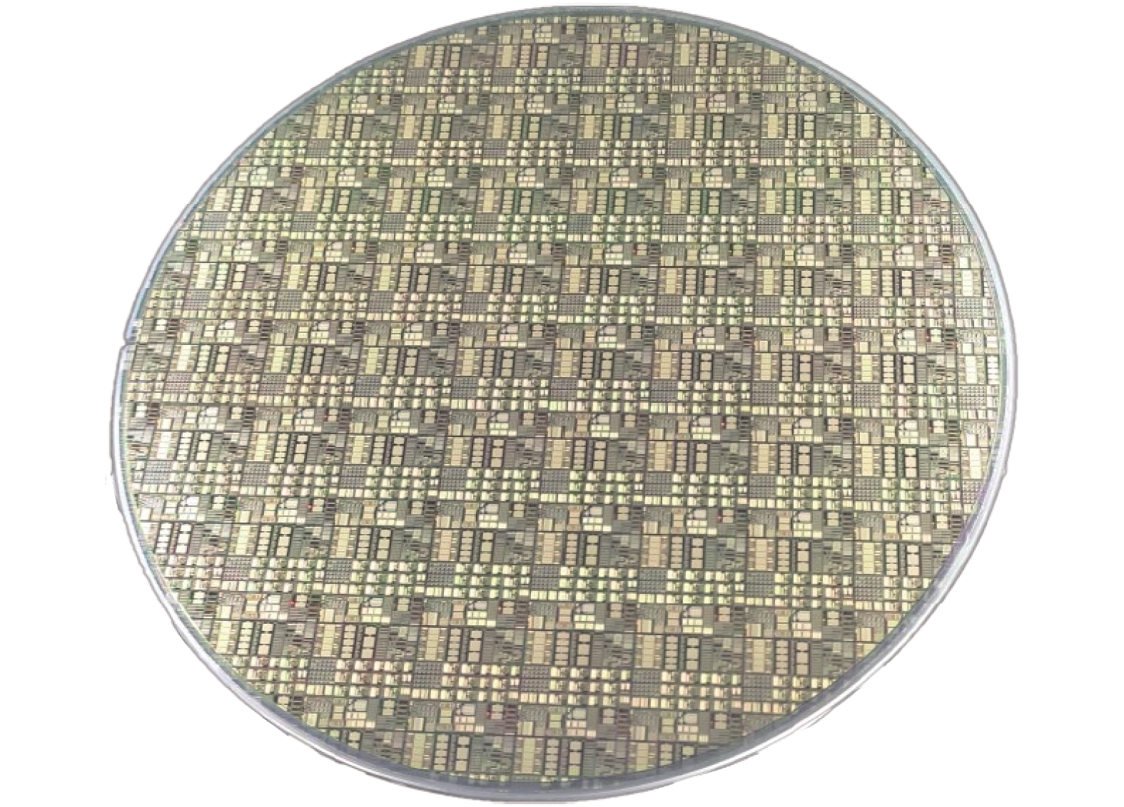
Fig. 1.  (Color online) Fabricated 200 mm GaN-on-SOI wafer with CMOS-compatible processing.

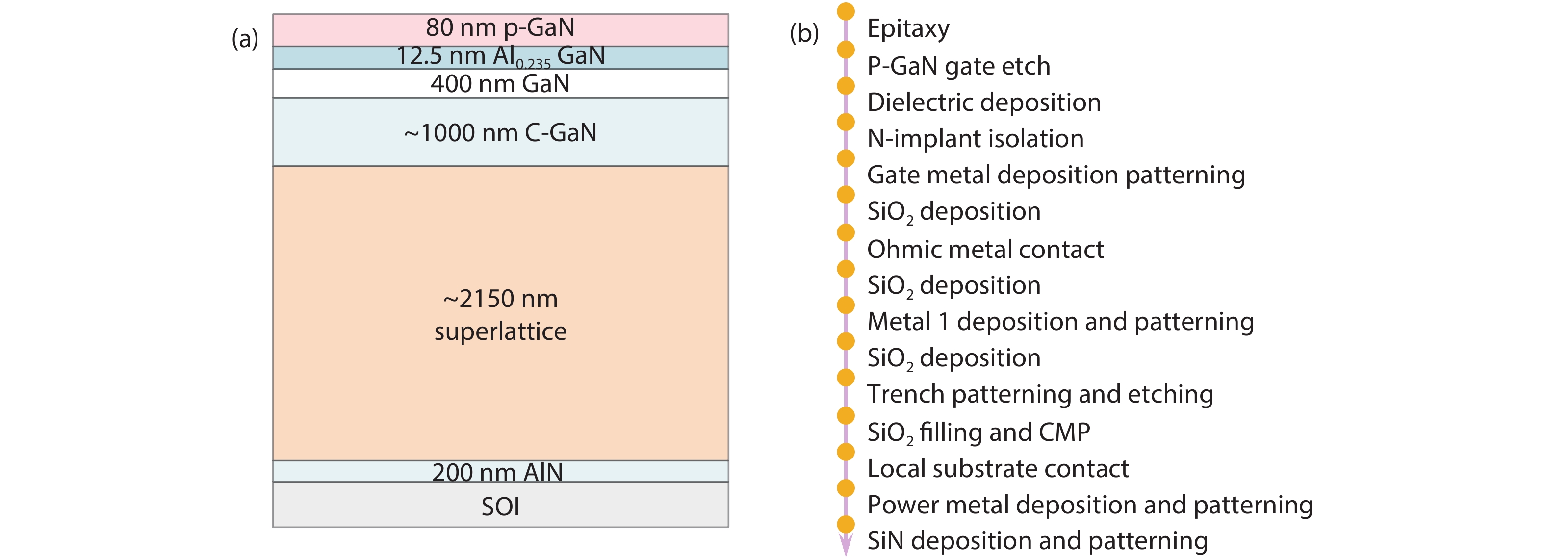
Fig. 2.  (Color online) (a) Schematic cross-section of the epitaxial layer stack and (b) processing flow.

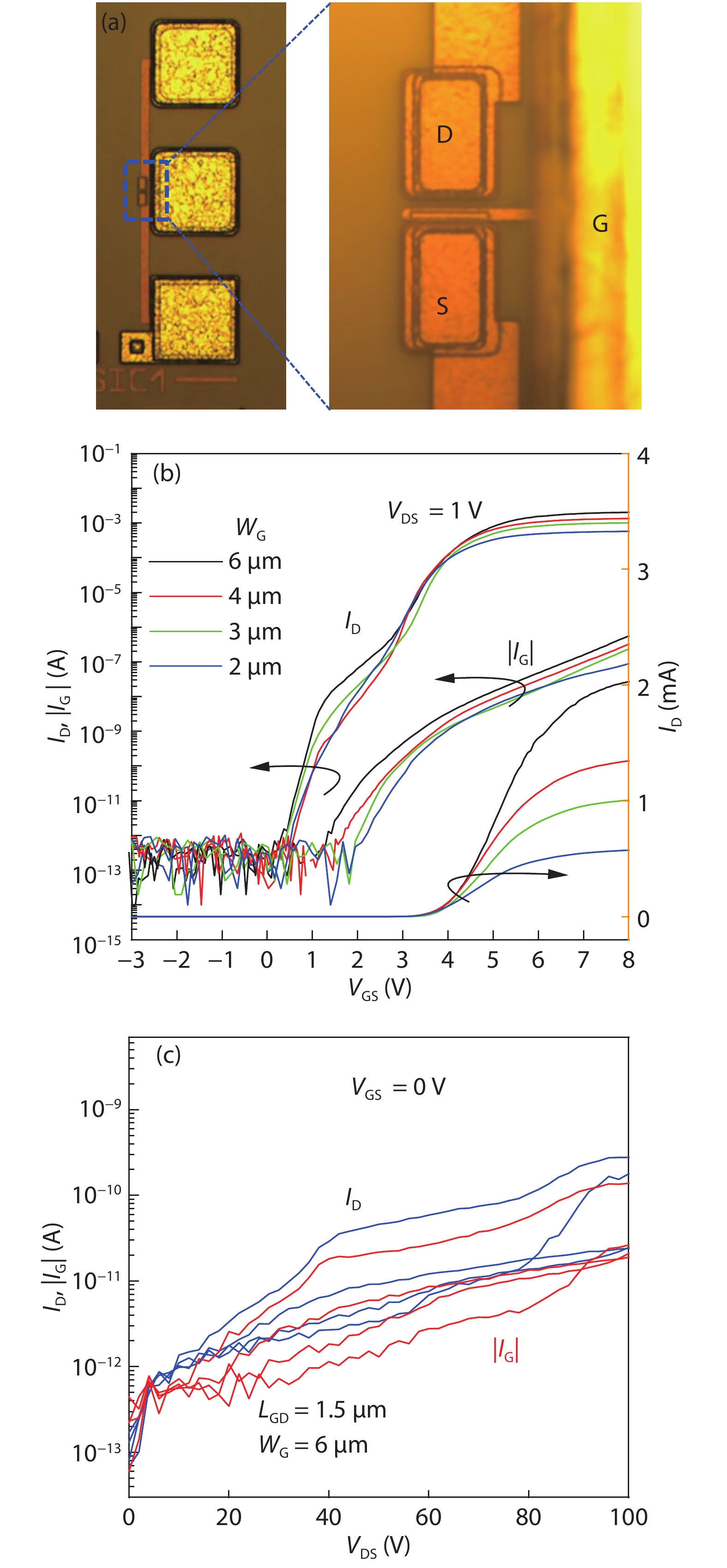
Fig. 3.  (Color online) (a) Microscope images, (b) transfer characteristics, and (c) OFF-state leakage characteristics of the logic HEMTs with LGD of 1.5 μm and WG scaling from 6 μm to 2 μm.

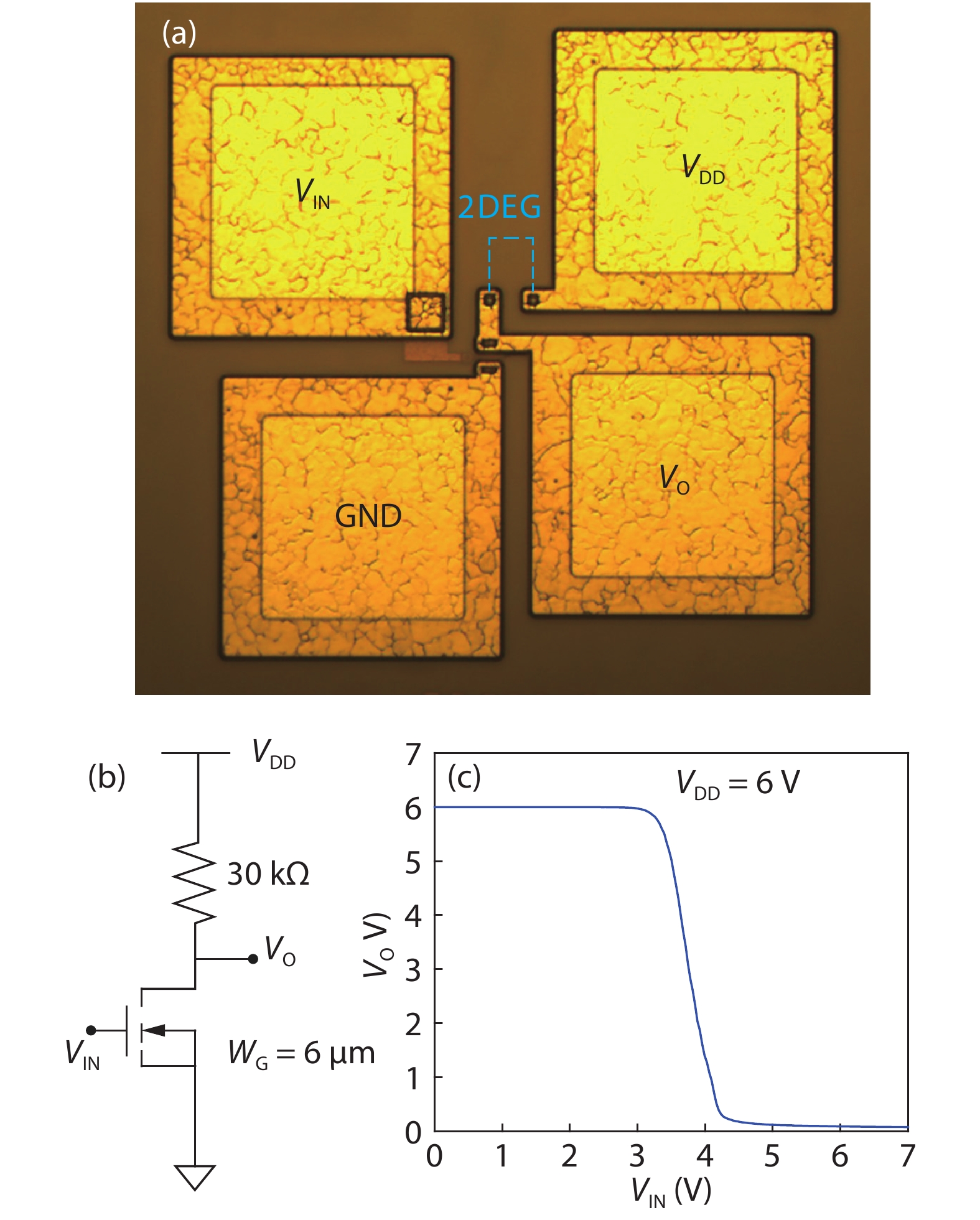
Fig. 4.  (Color online) (a) Microscope image, (b) schematic, and (c) measured voltage transfer characteristic (VTC) of the integrated RTL inverter.

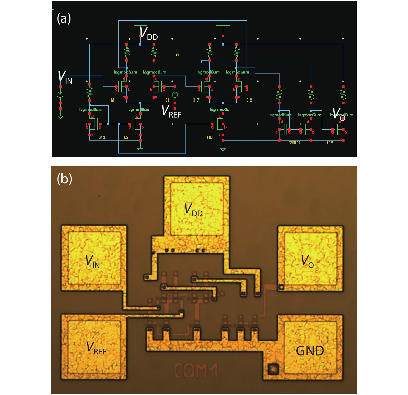
Fig. 5.  (Color online) (a) Comparator designed by RTL and (b) the microscope image of the processed comparator.

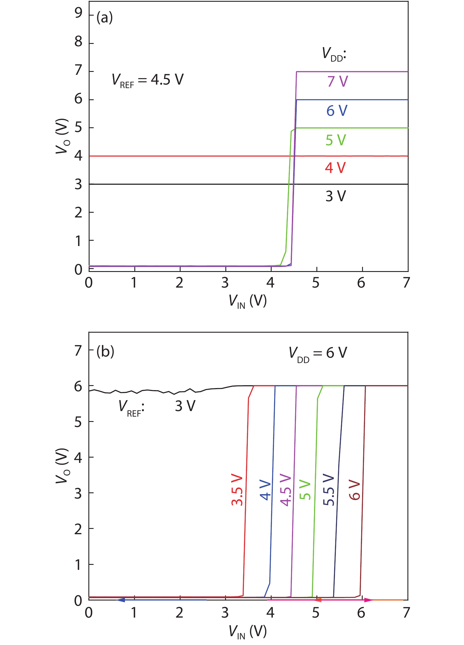
Fig. 6.  (Color online) (a) Voltage transfer characteristics of the comparator with (a) various VDD and (b) various reference voltage VREF.

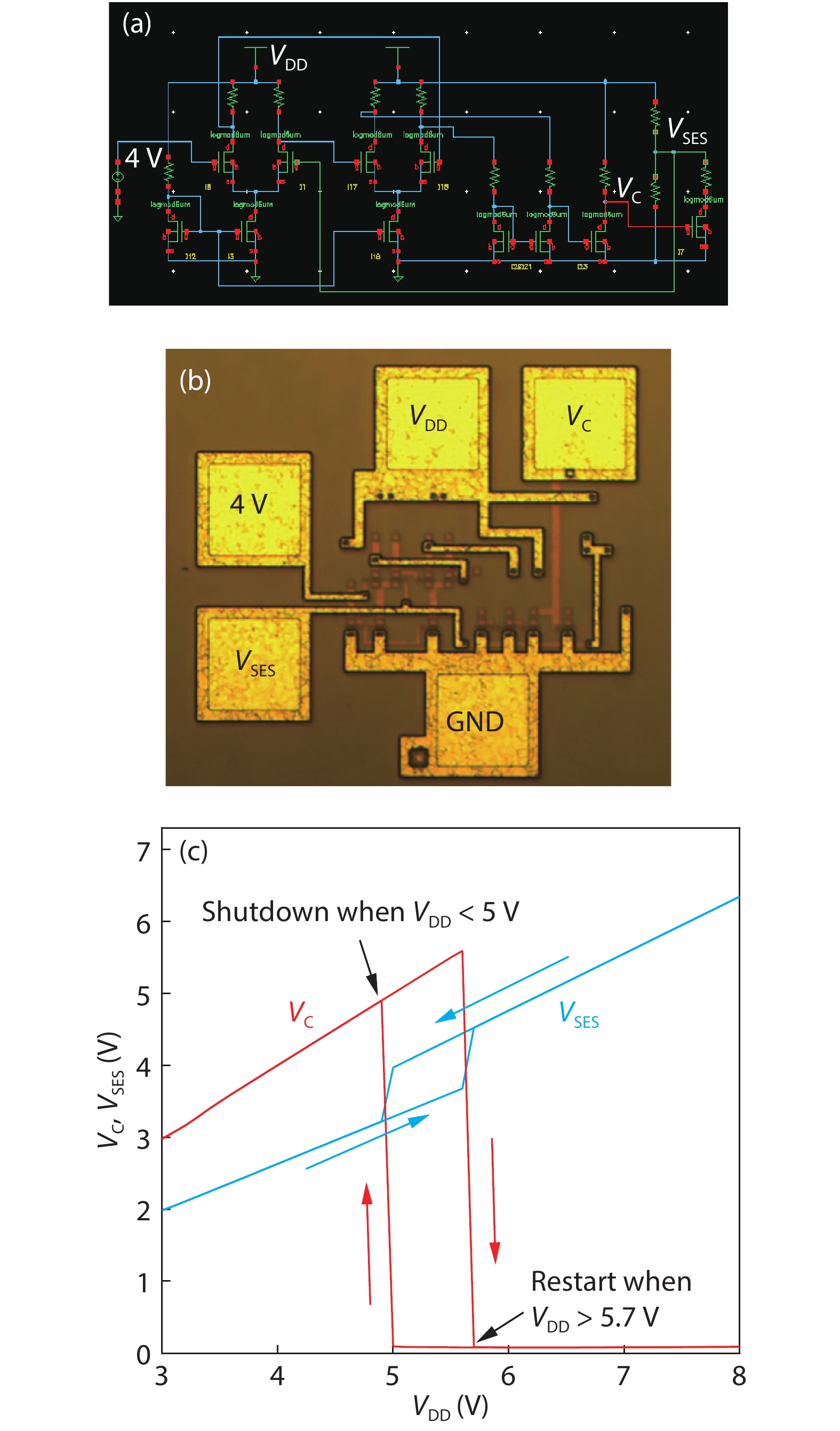
Fig. 7.  (Color online) (a) Undervoltage lockout GaN circuit, (b) layout, and (c) voltage transfer characteristics show the IC shuts down when VDD < 5 V and restarts when VDD > 5.7 V.

[1]
Dan K. GaN power IC technology: Past, present, and future. 2017 29th International Symposium on Power Semiconductor Devices and IC's (ISPSD), 2017, 19
[2]
Uemoto Y, Morita T, Ikoshi A, et al. GaN monolithic inverter IC using normally-off gate injection transistors with planar isolation on Si substrate. 2009 IEEE International Electron Devices Meeting (IEDM), 2009, 1
[3]
Moench S, Kallfass I, Reiner R, et al. Single-input GaN gate driver based on depletion-mode logic integrated with a 600 V GaN-on-Si power transistor. 2016 IEEE 4th Work Wide Bandgap Power Devices Appl Wipda, 2016, 204
[4]
Tang G, Kwan M H, Zhang Z, et al. High-speed, high-reliability GaN power device with integrated gate driver. Proc ISPSD, 2018, 76
[5]
Li X D, van Hove M, Zhao M, et al. 200 V enhancement-mode p-GaN HEMTs fabricated on 200 mm GaN-on-SOI with trench isolation for monolithic integration. IEEE Electron Device Lett, 2017, 38, 918 doi: 10.1109/LED.2017.2703304
[6]
Li X D, van Hove M, Zhao M, et al. Suppression of the backgating effect of enhancement-mode p-GaN HEMTs on 200-mm GaN-on-SOI for monolithic integration. IEEE Electron Device Lett, 2018, 39, 999 doi: 10.1109/LED.2018.2833883
[7]
Li X D, Geens K, Guo W M, et al. Demonstration of GaN integrated half-bridge with on-chip drivers on 200-mm engineered substrates. IEEE Electron Device Lett, 2019, 40, 1499 doi: 10.1109/LED.2019.2929417
[8]
Li X, Amirifar N, Geens K, et al. GaN-on-SOI: Monolithically integrated all-GaN ICs for power conversion. 2019 IEEE International Electron Devices Meeting (IEDM), 2019, 4.4.1
[9]
Li X D, van Hove M, Zhao M, et al. Investigation on carrier transport through AlN nucleation layer from differently doped Si(111) substrates. IEEE Trans Electron Devices, 2018, 65, 1721 doi: 10.1109/TED.2018.2810886
[10]
Li X D, Zhao M, Bakeroot B, et al. Buffer vertical leakage mechanism and reliability of 200-mm GaN-on-SOI. IEEE Trans Electron Devices, 2019, 66, 553 doi: 10.1109/TED.2018.2878457
[11]
Geens K, Li X D, Zhao M, et al. 650 V p-GaN gate power HEMTs on 200 mm engineered substrates. 2019 IEEE 7th Workshop on Wide Bandgap Power Devices and Applications (WiPDA), 2019, 292
[12]
Liu X S, Chen K J. GaN single-polarity power supply bootstrapped comparator for high-temperature electronics. IEEE Electron Device Lett, 2011, 32, 27 doi: 10.1109/LED.2010.2088376
[13]
van Hove M, Boulay S, Bahl S R, et al. CMOS process-compatible high-power low-leakage AlGaN/GaN MISHEMT on silicon. IEEE Electron Device Lett, 2012, 33, 667 doi: 10.1109/LED.2012.2188016
[14]
Wu T L, Marcon D, You S Z, et al. Forward bias gate breakdown mechanism in enhancement-mode p-GaN gate AlGaN/GaN high-electron mobility transistors. IEEE Electron Device Lett, 2015, 36, 1001 doi: 10.1109/LED.2015.2465137
[15]
[16]
Li X D, Bakeroot B, Wu Z C, et al. Observation of dynamic V TH of p-GaN gate HEMTs by fast sweeping characterization. IEEE Electron Device Lett, 2020, 41, 577 doi: 10.1109/LED.2020.2972971
  • Search

    Advanced Search >>

    GET CITATION

    shu

    Export: BibTex EndNote

    Article Metrics

    Article views: 4285 Times PDF downloads: 149 Times Cited by: 0 Times

    History

    Received: 01 June 2020 Revised: 28 June 2020 Online: Accepted Manuscript: 22 September 2020Uncorrected proof: 24 September 2020Published: 08 February 2021

    Catalog

      Email This Article

      User name:
      Email:*请输入正确邮箱
      Code:*验证码错误
      Xiangdong Li, Karen Geens, Nooshin Amirifar, Ming Zhao, Shuzhen You, Niels Posthuma, Hu Liang, Guido Groeseneken, Stefaan Decoutere. Integration of GaN analog building blocks on p-GaN wafers for GaN ICs[J]. Journal of Semiconductors, 2021, 42(2): 024103. doi: 10.1088/1674-4926/42/2/024103 ****X D Li, K Geens, N Amirifar, M Zhao, S Z You, N Posthuma, H Liang, G Groeseneken, S Decoutere, Integration of GaN analog building blocks on p-GaN wafers for GaN ICs[J]. J. Semicond., 2021, 42(2): 024103. doi: 10.1088/1674-4926/42/2/024103.
      Citation:
      Xiangdong Li, Karen Geens, Nooshin Amirifar, Ming Zhao, Shuzhen You, Niels Posthuma, Hu Liang, Guido Groeseneken, Stefaan Decoutere. Integration of GaN analog building blocks on p-GaN wafers for GaN ICs[J]. Journal of Semiconductors, 2021, 42(2): 024103. doi: 10.1088/1674-4926/42/2/024103 ****
      X D Li, K Geens, N Amirifar, M Zhao, S Z You, N Posthuma, H Liang, G Groeseneken, S Decoutere, Integration of GaN analog building blocks on p-GaN wafers for GaN ICs[J]. J. Semicond., 2021, 42(2): 024103. doi: 10.1088/1674-4926/42/2/024103.

      Integration of GaN analog building blocks on p-GaN wafers for GaN ICs

      DOI: 10.1088/1674-4926/42/2/024103
      More Information
      • Xiangdong Li:received the B.S and M.S. degrees in microelectronics from Xidian University, Xi’an, China, in 2013 and 2016, respectively, and the Ph.D degree with the Department of Electrical Engineering, Katholieke Universiteit Leuven, Leuven, Belgium, in 2020. From 2016 to 2020, he was also with the GaN Group, IMEC, Leuven, Belgium, as a Ph.D researcher. He focuses on GaN materials, devices, reliabilities, and circuits
      • Corresponding author: lixiangdong28@126.com
      • Received Date: 2020-06-01
      • Revised Date: 2020-06-28
      • Published Date: 2021-02-10

      Catalog

        /

        DownLoad:  Full-Size Img  PowerPoint
        Return
        Return