| Citation: |
Swagata Samanta, Jue Wang, Edward Wasige. Development of a simple two-step lithography fabrication process for resonant tunneling diode using air-bridge technology[J]. Journal of Semiconductors, 2023, 44(11): 114101. doi: 10.1088/1674-4926/44/11/114101
****
S Samanta, J Wang, E Wasige. Development of a simple two-step lithography fabrication process for resonant tunneling diode using air-bridge technology[J]. J. Semicond, 2023, 44(11): 114101. doi: 10.1088/1674-4926/44/11/114101
|
Development of a simple two-step lithography fabrication process for resonant tunneling diode using air-bridge technology
DOI: 10.1088/1674-4926/44/11/114101
More Information
-
Abstract
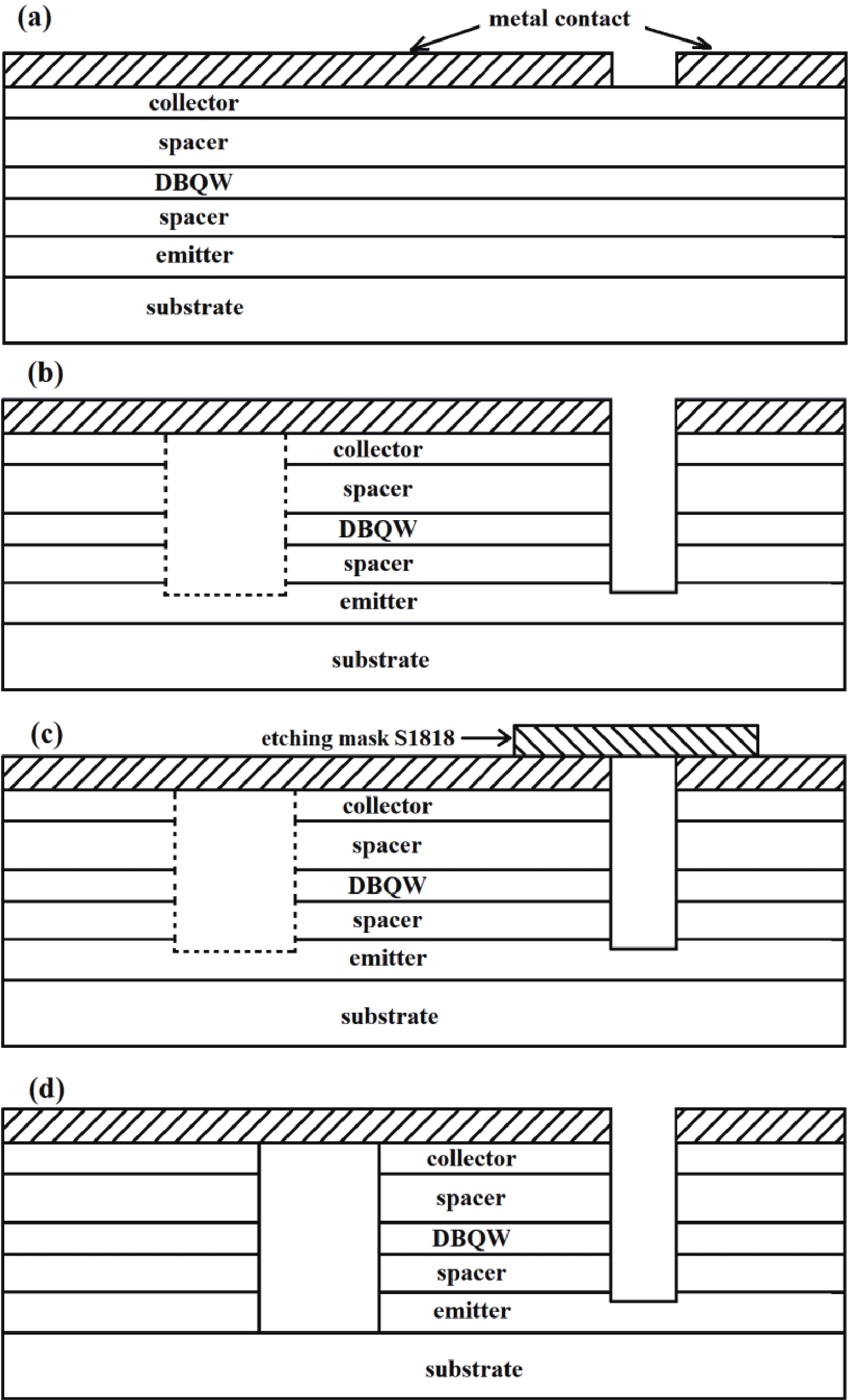
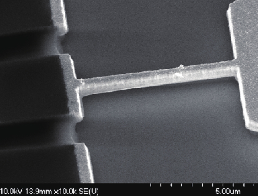
This article reports on the development of a simple two-step lithography process for double barrier quantum well (DBQW) InGaAs/AlAs resonant tunneling diode (RTD) on a semi-insulating indium phosphide (InP) substrate using an air-bridge technology. This approach minimizes processing steps, and therefore the processing time as well as the required resources. It is particularly suited for material qualification of new epitaxial layer designs. A DC performance comparison between the proposed process and the conventional process shows approximately the same results. We expect that this novel technique will aid in the recent and continuing rapid advances in RTD technology. -
References
[1] Sun J P, Haddad G I, Mazumder P, et al. Resonant tunneling diodes: Models and properties. Proc IEEE, 1998, 86, 641 doi: 10.1109/5.663541[2] Sugiyama H, Yokoyama H, Teranishi A, et al. Extremely high peak current densities of over 1 × 10⁶ A/cm2 in InP-based InGaAs/AlAs resonant tunneling diodes grown by metal–organic vapor-phase epitaxy. Jpn J Appl Phys, 2010, 49, 051201 doi: 10.1143/JJAP.49.051201[3] Shimizu N, Shinagawa M, Yamamoto M, et al. In0.53Ga0.47As/AlAs resonant tunnelling diodes with switching time of 1.5 ps. Electron Lett, 1995, 31, 1695 doi: 10.1049/el:19951102[4] Smet J H, Broekaert T P E, Fonstad C G. Peak-to-valley current ratios as high as 50 : 1 at room temperature in pseudomorphic In0.53Ga0.47As/AlAs/InAs resonant tunneling diodes. J Appl Phys, 1992, 71, 2475 doi: 10.1063/1.351085[5] Huang C I, Paulus M J, Bozada C A, et al. AlGaAs/GaAs double barrier diodes with high peak-to-valley current ratio. Appl Phys Lett, 1987, 51, 121 doi: 10.1063/1.98588[6] Al-Khalidi A, Alharbi K H, Wang J, et al. Resonant tunneling diode terahertz sources with up to 1 mW output power in the J-band. IEEE Trans THz Sci Technol, 2020, 10, 150 doi: 10.1109/TTHZ.2019.2959210[7] Feiginov M, Sydlo C, Cojocari O, et al. Resonant-tunnelling-diode oscillators operating at frequencies above 1.1 THz. Appl Phys Lett, 2011, 99, 233506 doi: 10.1063/1.3667191[8] Asada M, Suzuki S. Room-temperature oscillation of resonant tunneling diodes close to 2 THz and their functions for various applications. J Infrared Millim Terahertz Waves, 2016, 37, 1185 doi: 10.1007/s10762-016-0321-6[9] Maekawa T, Kanaya H, Suzuki S, et al. Oscillation up to 1.92 THz in resonant tunneling diode by reduced conduction loss. Appl Phys Express, 2016, 9, 024101 doi: 10.7567/APEX.9.024101[10] Zhang W K, Watson S, Figueiredo J, et al. Optical direct intensity modulation of a 79GHz resonant tunneling diode-photodetector oscillator. Opt Express, 2019, 27, 16791 doi: 10.1364/OE.27.016791[11] Paoloni C, Basu R P, Billa L R, et al. Long-range millimeter wave wireless links enabled by traveling wave tubes and resonant tunnelling diodes. IET Microw Antennas Propag, 2020, 2110 doi: 10.1049/iet-map.2020.0084[12] Maezawa K. Resonant tunneling diodes and their application to high-speed circuits. IEEE Compound Semiconductor Integrated Circuit Symposium, 2005, 97. doi: 10.1109/CSICS.2005.1531772[13] Romeira B, Pessoa L, Salgado H, et al. Photo-detectors integrated with resonant tunneling diodes. Sensors, 2013, 13, 9464 doi: 10.3390/s130709464[14] Pfenning A, Hartmann F, Langer F B, et al. Sensitivity of resonant tunneling diode photodetectors. Nanotechnology, 2016, 27, 355202 doi: 10.1088/0957-4484/27/35/355202[15] Oshima N, Hashimoto K, Suzuki S, et al. Terahertz wireless data transmission with frequency and polarization division multiplexing using resonant-tunneling-diode oscillators. IEEE Trans Terahertz Sci Technol, 2017, 7, 593 doi: 10.1109/TTHZ.2017.2720470[16] J. Wang J, Al-Khalidi A, Wang L, et al. 15-Gb/s 50-cm wireless link using a high-power compact III–V 84-GHz transmitter. IEEE Transactions on Microwave Theory and Techniques, 2018, 66, 4698 doi: 10.1109/TMTT.2018.2859983[17] Weng Q C, An Z H, Zhang B, et al. Quantum dot single-photon switches of resonant tunneling current for discriminating-photon-number detection. Sci Rep, 2015, 5, 1 doi: 10.1038/srep09389[18] Pfenning A, Jurkat J, Naranjo A, et al. Resonant tunneling diode photon number resolving single-photon detectors. SPIE Optical Engineering + Applications Proc SPIE 11128, Infrared Remote Sensing and Instrumentation XXVII, 2019, 11128, 47 doi: 10.1117/12.2529929[19] Duan S K, Hu X F, Wang L D, et al. Resonant tunneling diodes-based cellular nonlinear networks with fault tolerance analysis. Math Probl Eng, 2013, 2013, 1 doi: 10.1155/2013/170202[20] Romeira B, Figueiredo J M L, Javaloyes J. NanoLEDs for energy-efficient and gigahertz-speed spike-based sub-λ neuromorphic nanophotonic computing. Nanophotonics, 2020, 9, 4149 doi: 10.1515/nanoph-2020-0177[21] Ortega I, Piro O, Romeira B, et al. Bursting and excitability in neuromorphic resonant tunneling diodes. 2021 Conference on Lasers and Electro-Optics Europe & European Quantum Electronics Conference (CLEO/Europe-EQEC), Munich, Germany, 2021, 1 doi: 10.1109/CLEO/Europe-EQEC52157.2021.9542172[22] Esaki L, Tsu R. Superlattice and negative differential conductivity in semiconductors. IBM J Res Dev, 1970, 14, 61 doi: 10.1147/rd.141.0061[23] Tsu R, Esaki L. Tunneling in a finite superlattice. Appl Phys Lett, 1973, 22, 562 doi: 10.1063/1.1654509[24] Chang L L, Esaki L, Tsu R. Resonant tunneling in semiconductor double barriers. Appl Phys Lett, 1974, 24, 593 doi: 10.1063/1.1655067[25] Tsuchiya M, Sakaki H, Yoshino J. Room temperature observation of differential negative resistance in an AlAs/GaAs/AlAs resonant tunneling diode. Jpn J Appl Phys, 1985, 24, L466 doi: 10.1143/JJAP.24.L466[26] Wang J, Al-Khalidi A, Alharbi K, et al. High performance resonant tunneling diode oscillators as terahertz sources. 2016 46th European Microwave Conference (EuMC), 2017, 341 doi: 10.1109/EuMC.2016.7824348[27] Wang J, Al-Khalidi A, Cornescu A, et al. Design, fabrication and characterisation of RTD terahertz oscillators. 2019 European Microwave Conference in Central Europe (EuMCE), 2019, 261[28] Zawawi M A M, Sexton J, Missous M. Advanced InGaAs/AlAs RTD with high current density incorporating multi-bridge (air-bridge) emitter design. UK Semiconductor 2012 Conference, 2012, 7[29] Muttlak S G, Abdulwahid O S, Sexton J, et al. InGaAs/AlAs resonant tunneling diodes for THz applications: An experimental investigation. IEEE J Electron Devices Soc, 2018, 6, 254 doi: 10.1109/JEDS.2018.2797951[30] Zawawi M A M. Advanced In0.8Ga0.2As/AlAs resonant tunneling diodes for applications in integrated mm-waves MMIC oscillators. Ph. D Thesis, University of Manchester, 2015[31] Han C L, Chen C, Zou P H, et al. InP-base resonant tunneling diodes. J Semicond, 2009, 30, 064001 doi: 10.1088/1674-4926/30/6/064001[32] Wang W, Sun H, Teng T, et al. High peak-to-valley current ratio In0.53Ga0.47As/AlAs resonant tunneling diode with a high doping emitter. J Semicond, 2012, 33, 124002 doi: 10.1088/1674-4926/33/12/124002 -
Proportional views


 DownLoad:


 Swagata Samanta:(FIETE, MIEEE) received her Ph.D degree from Indian Institute of Technology Kharagpur in 2018. She continued her research as a postdoctoral fellow at the Centre for Nano Science and Engineering, Indian Institute of Science Bangalore and then at James Watt School of Engineering, University of Glasgow, UK. Presently, she is an Assistant Professor in the Department of Electronics and Communication Engineering at SRM University, Andhra Pradesh, India. Her research interests are interdisciplinary and encompass a broad range of areas, including novel on-chip nanophotonic and nanoelectronic devices, integrated optics, neuromorphics, VLSI systems, image/video processing, and artificial intelligence
 Jue Wang:received his Ph.D degree in Electronics and Electrical Engineering in 2014 from the University of Glasgow, Glasgow, UK. Since 2014, he has been working on resonant tunneling diode based terahertz oscillator design as a Postdoctoral Researcher. His research interests include high-power terahertz devices and terahertz applications including wireless communications, imaging, etc
 Edward Wasige:(S’97–M’99) received his B.Sc. (Eng.) degree in Electrical Engineering in 1988 from the University of Nairobi, Nairobi, Kenya, M.Sc. (Eng.) degree in microelectronic systems and telecommunications in 1990 from the University of Liverpool, Liverpool, UK, and Ph.D degree in Electrical Engineering from Kassel University, Kassel, Germany, in 1999. Prior to becoming a Lecturer with the University of Glasgow, Glasgow, UK, in 2002, he was a UNESCO Postdoctoral Fellow with the Technion—Israel Institute of Technology. His research interests include compound semiconductor micro-/nanoelectronics and applications with focus on gallium nitride electronics and resonant tunneling diode based terahertz electronics


