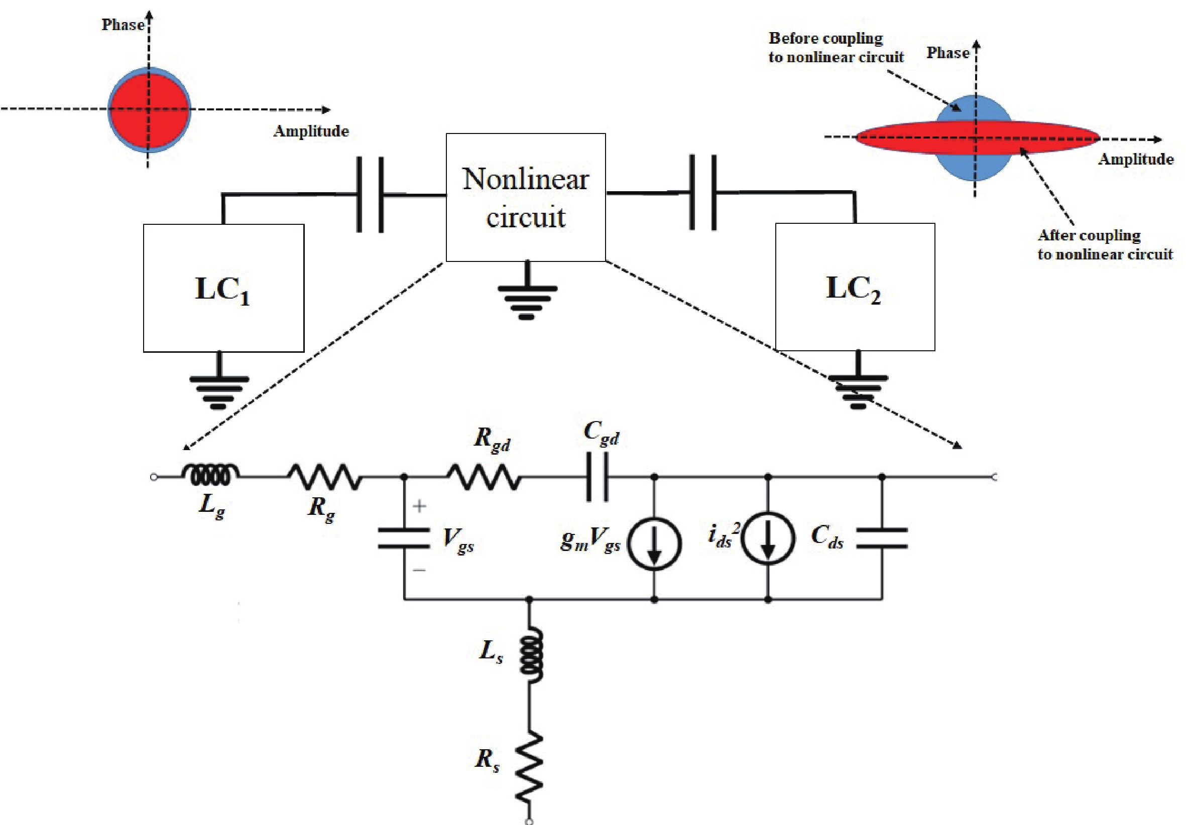
Fig. 1.
(Color online) Schematic of the system containing two external oscillators coupling through a nonlinear device, inset figure: nonlinear device internal circuit.
ARTICLES
Corresponding author: Ahmad Salmanogli, salmanogli@cankaya.edu.tr
Abstract: This study focuses on generating and manipulating squeezed states with two external oscillators coupled by an InP HEMT operating at cryogenic temperatures. First, the small-signal nonlinear model of the transistor at high frequency at 5 K is analyzed using quantum theory, and the related Lagrangian is theoretically derived. Subsequently, the total quantum Hamiltonian of the system is derived using Legendre transformation. The Hamiltonian of the system includes linear and nonlinear terms by which the effects on the time evolution of the states are studied. The main result shows that the squeezed state can be generated owing to the transistor’s nonlinearity; more importantly, it can be manipulated by some specific terms introduced in the nonlinear Hamiltonian. In fact, the nonlinearity of the transistors induces some effects, such as capacitance, inductance, and second-order transconductance, by which the properties of the external oscillators are changed. These changes may lead to squeezing or manipulating the parameters related to squeezing in the oscillators. In addition, it is theoretically derived that the circuit can generate two-mode squeezing. Finally, second-order correlation (photon counting statistics) is studied, and the results demonstrate that the designed circuit exhibits antibunching, where the quadrature operator shows squeezing behavior.
Keywords: quantum theory, squeezed state, cryogenic low noise amplifier, InP HEMT
| [1] |
Walls D F. Squeezed states of light. Nature, 1983, 306, 141 doi: 10.1038/306141a0
|
| [2] |
Mandel L. Squeezed states and sub-poissonian photon statistics. Phys Rev Lett, 1982, 49, 136 doi: 10.1103/PhysRevLett.49.136
|
| [3] |
Rodrigues H, Portes D Jr, Duarte S B, et al. Squeezing in coupled oscillators having neither nonlinear terms nor time-dependent parameters. Braz J Phys, 2001, 31, 562 doi: 10.1590/S0103-97332001000400006
|
| [4] |
Friberg S, Mandel L. Production of squeezed states by combination of parametric down-conversion and harmonic generation. Opt Commun, 1984, 48, 439 doi: 10.1016/0030-4018(84)90041-5
|
| [5] |
Mollow B R, Glauber R J. Quantum theory of parametric amplification. I. Phys Rev, 1967, 160, 1076 doi: 10.1103/PhysRev.160.1076
|
| [6] |
Shahriar M S, Hemmer P R. Generation of squeezed states and twin beams via non-degenerate four-wave mixing in a Λ system. Opt Commun, 1998, 158, 273 doi: 10.1016/S0030-4018(98)00528-8
|
| [7] |
Lvovsky A I. Squeezed light. In: Photonics: Scientific foundations, technology and applications. John Wiley & Sons, Inc, 2015, 121
|
| [8] |
Yuen H P, Shapiro J H. Generation and detection of two-photon coherent states in degenerate four-wave mixing. Opt Lett, 1979, 4, 334 doi: 10.1364/OL.4.000334
|
| [9] |
Hirano T, Matsuoka M. Broadband squeezing of light by pulse excitation. Opt Lett, 1990, 15, 1153 doi: 10.1364/OL.15.001153
|
| [10] |
Breitenbach G, Schiller S, Mlynek J. Measurement of the quantum states of squeezed light. Nature, 1997, 387, 471 doi: 10.1038/387471a0
|
| [11] |
Yamamoto Y, Machida S, Richardson W H. Photon number squeezed states in semiconductor lasers. Science, 1992, 255, 1219 doi: 10.1126/science.255.5049.1219
|
| [12] |
Raiford M T. Statistical dynamics of quantum oscillators and parametric amplification in a single mode. Phys Rev A, 1970, 2, 1541 doi: 10.1103/PhysRevA.2.1541
|
| [13] |
Davidovich L. Sub-Poissonian processes in quantum optics. Rev Modern Phys, 1996, 68, 127 doi: 10.1103/RevModPhys.68.127
|
| [14] |
Scully M O, Zubairy M S. Quantum Optics. Cambridge: : Cambridge University Press, 1997
|
| [15] |
Salmanogli A, Gokcen D. Entanglement sustainability improvement using optoelectronic converter in quantum radar (interferometric object-sensing). IEEE Sens J, 2021, 21, 9054 doi: 10.1109/JSEN.2021.3052256
|
| [16] |
Salmanogli A, Gokcen D, Gecim H S. Entanglement sustainability in quantum radar. IEEE J Sel Top Quantum Electron, 2020, 26, 1 doi: 10.1109/JSTQE.2020.3020620
|
| [17] |
Barzanjeh S, Pirandola S, Vitali D, et al. Microwave quantum illumination using a digital receiver. Sci Adv, 2020, 6, eabb0451 doi: 10.1126/sciadv.abb0451
|
| [18] |
Barzanjeh S, Guha S, Weedbrook C, et al. Microwave quantum illumination. Phys Rev Lett, 2015, 114, 080503 doi: 10.1103/PhysRevLett.114.080503
|
| [19] |
Salmanogli A, Gokcen D. Design of quantum sensor to duplicate European Robins navigational system. Sens Actuat A Phys, 2021, 322, 112636 doi: 10.1016/j.sna.2021.112636
|
| [20] |
Salmanogli A, Gokcen D, Gecim H S. Entanglement of optical and microcavity modes by means of an optoelectronic system. Phys Rev Appl, 2019, 11, 024075 doi: 10.1103/PhysRevApplied.11.024075
|
| [21] |
Aparin V, Larson L E. Modified derivative superposition method for linearizing FET low-noise amplifiers. IEEE Trans Microwave Theory Techn, 2005, 53, 571 doi: 10.1109/TMTT.2004.840635
|
| [22] |
Ganesan S, Sanchez-Sinencio E, Silva-Martinez J. A highly linear low-noise amplifier. IEEE Trans Microwave Theory Techn, 2006, 54, 4079 doi: 10.1109/TMTT.2006.885889
|
| [23] |
Hamaizia Z, Sengouga N, Missous M, et al. A 0.4dB noise figure wideband low-noise amplifier using a novel InGaAs/InAlAs/InP device. Mater Sci Semicond Process, 2011, 14, 89 doi: 10.1016/j.mssp.2010.12.003
|
| [24] |
Yurke B, Roukes M L, Movshovich R, et al. A low-noise series-array Josephson junction parametric amplifier. Appl Phys Lett, 1996, 69, 3078 doi: 10.1063/1.116845
|
| [25] |
Schleeh J, Alestig G, Halonen J, et al. Ultralow-power cryogenic InP HEMT with minimum noise temperature of 1 K at 6 GHz. IEEE Electron Device Lett, 2012, 33, 664 doi: 10.1109/LED.2012.2187422
|
| [26] |
Cha E, Wadefalk N, Moschetti G, et al. A 300-µW cryogenic HEMT LNA for quantum computing. 2020 IEEE/MTT-S International Microwave Symposium (IMS), 2020, 1299
|
| [27] |
Wadefalk N, Mellberg A, Angelov I, et al. Cryogenic wide-band ultra-low-noise if amplifiers operating at ultra-low DC power. IEEE Trans Microwave Theory Techn, 2003, 51, 1705 doi: 10.1109/TMTT.2003.812570
|
| [28] |
Salmanogli A, Gecim H S. Design of the ultra-low noise amplifier for quantum applications. arXiv preprint arXiv: 2111.15358, 2021
|
| [29] |
Salmanogli A. Entangled microwave photons generation using cryogenic low noise amplifier (transistor nonlinearity effects). Quantum Sci Technol, 2022, 7, 045026 doi: 10.1088/2058-9565/ac8bf0
|
| [30] |
Fan X H, Zhang H, SÁnchez-Sinencio E. A noise reduction and linearity improvement technique for a differential cascode LNA. IEEE J Solid State Circuits, 2008, 43, 588 doi: 10.1109/JSSC.2007.916584
|
| [31] |
Cha E, Moschetti G, Wadefalk N, et al. Two-finger InP HEMT design for stable cryogenic operation of ultra-low-noise Ka-and Q-band LNAs. IEEE Trans Microwave Theory Tech, 2017, 65, 5171-80 doi: 10.1109/TMTT.2017.2765318
|
| [32] |
Cha E, Wadefalk N, Moschetti G, et al. InP HEMTs for sub-mW cryogenic low-noise amplifiers. IEEE Electron Device Lett, 2020, 41, 1005 doi: 10.1109/LED.2020.3000071
|
| [33] |
Mellberg A, Wadefalk N, Angelov I, et al. Cryogenic 2-4 GHz ultra low noise amplifier. 2004 IEEE MTT-S International Microwave Symposium Digest, 2004, 161
|
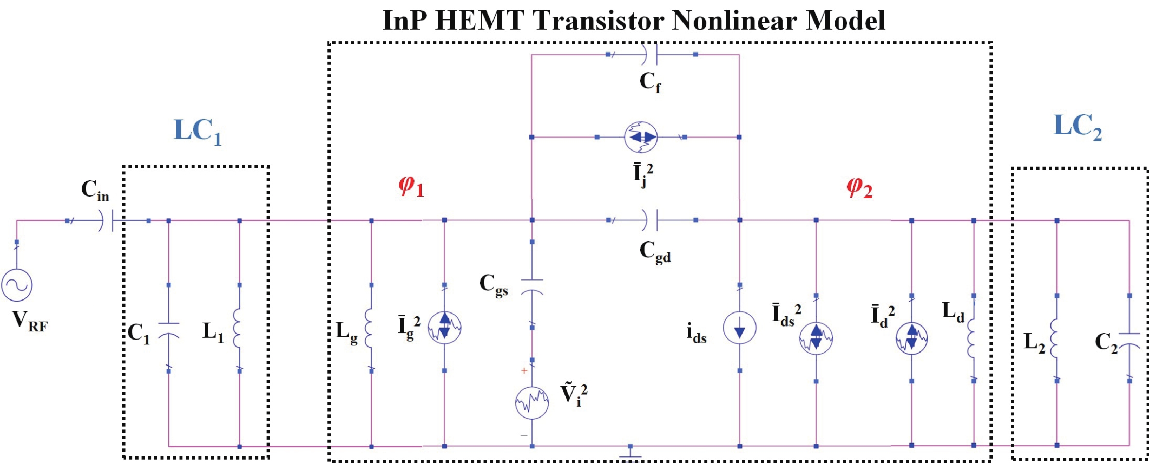
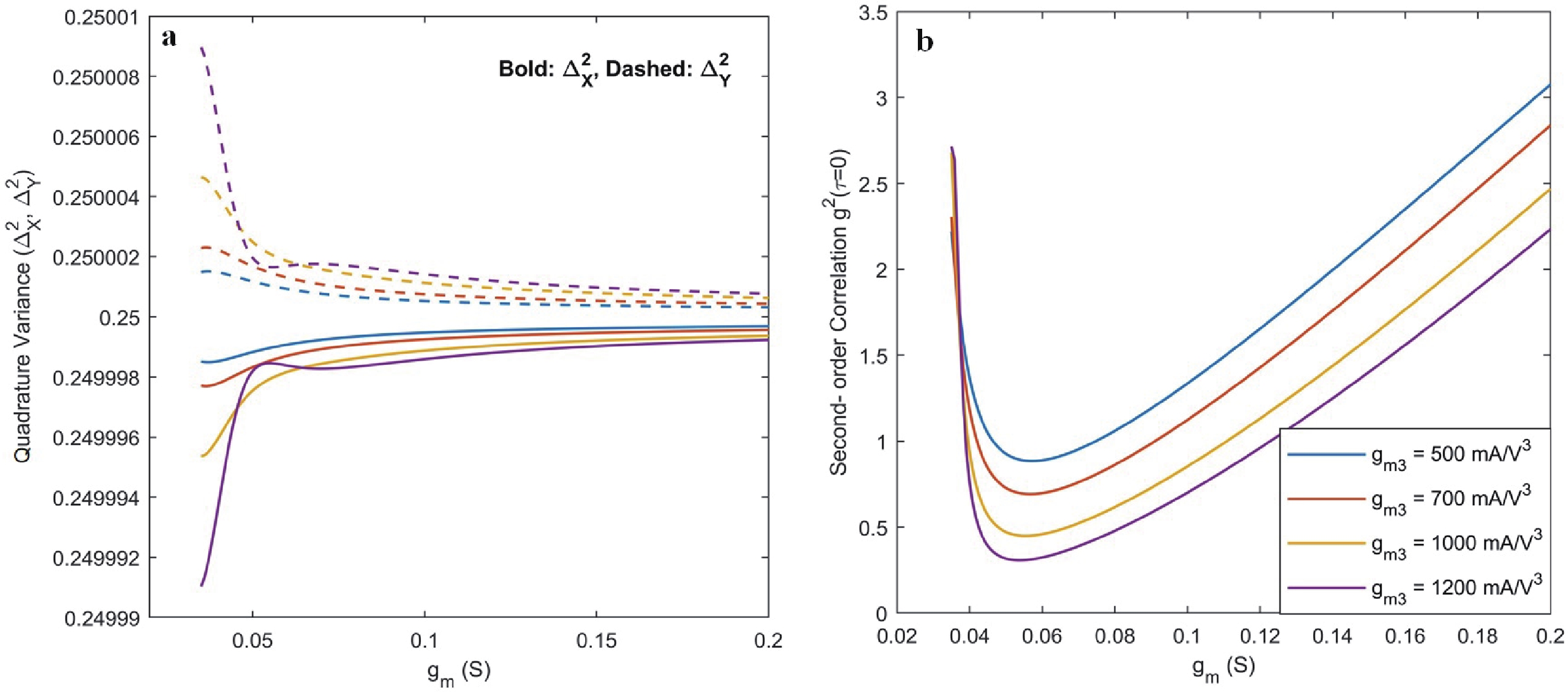
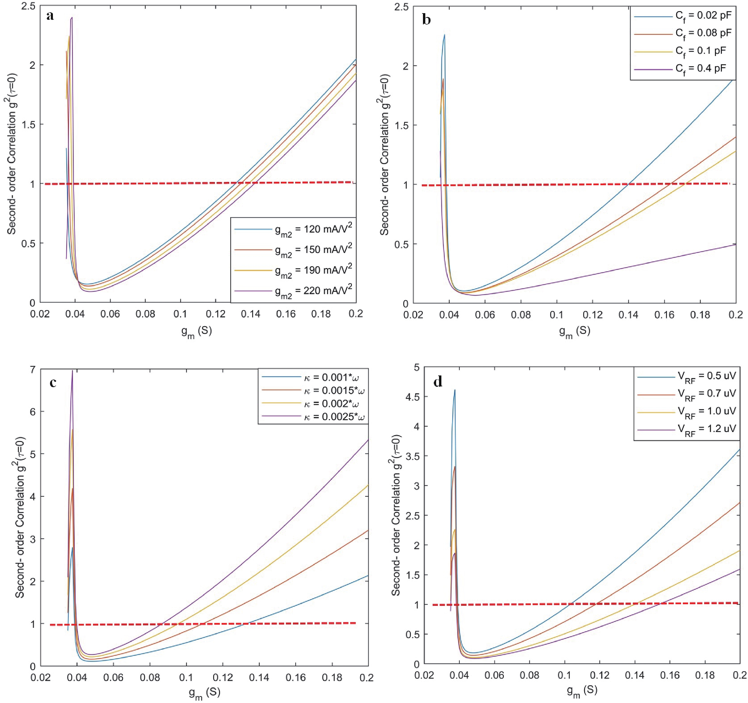
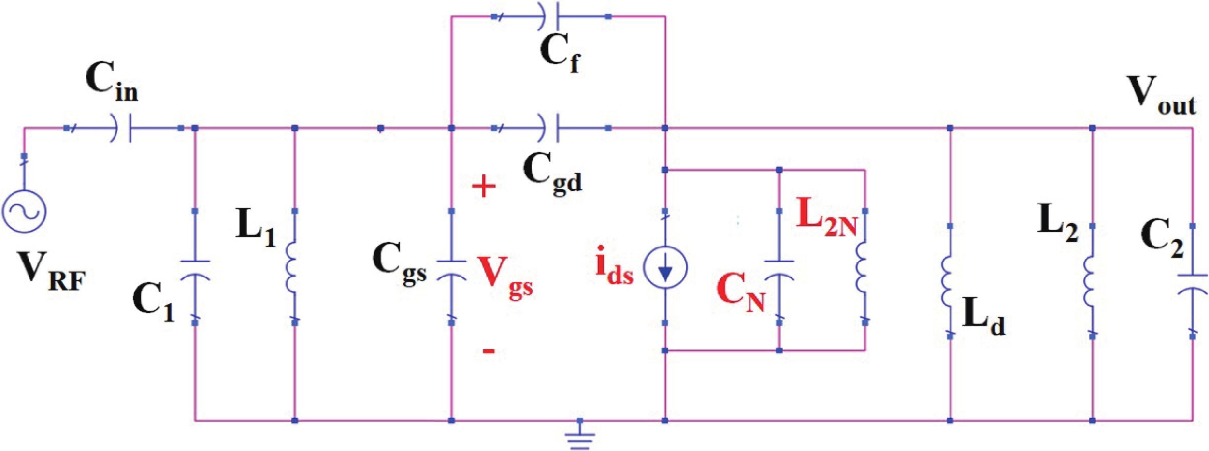
Table 1. Values for the small signal model of the 2 × 50 μm InP HEMT at 5 K [31-33].
| Stands for | Value | |
| Rg | Gate resistance | 0.3 Ω |
| Lg | Gate inductance | 75 pH |
| Ld | Drain inductance | 70 pH |
| Cgs | Gate–source capacitance | 69 fF |
| Cds | Drain–source capacitance | 29 fF |
| Cgd | Gate–drain capacitance | 19 fF |
| Rgs | Gate-source resistance | 4 Ω |
| Rgd | Gate–drain resistance | 35 Ω |
 DownLoad: CSV
| [1] |
Walls D F. Squeezed states of light. Nature, 1983, 306, 141 doi: 10.1038/306141a0
|
| [2] |
Mandel L. Squeezed states and sub-poissonian photon statistics. Phys Rev Lett, 1982, 49, 136 doi: 10.1103/PhysRevLett.49.136
|
| [3] |
Rodrigues H, Portes D Jr, Duarte S B, et al. Squeezing in coupled oscillators having neither nonlinear terms nor time-dependent parameters. Braz J Phys, 2001, 31, 562 doi: 10.1590/S0103-97332001000400006
|
| [4] |
Friberg S, Mandel L. Production of squeezed states by combination of parametric down-conversion and harmonic generation. Opt Commun, 1984, 48, 439 doi: 10.1016/0030-4018(84)90041-5
|
| [5] |
Mollow B R, Glauber R J. Quantum theory of parametric amplification. I. Phys Rev, 1967, 160, 1076 doi: 10.1103/PhysRev.160.1076
|
| [6] |
Shahriar M S, Hemmer P R. Generation of squeezed states and twin beams via non-degenerate four-wave mixing in a Λ system. Opt Commun, 1998, 158, 273 doi: 10.1016/S0030-4018(98)00528-8
|
| [7] |
Lvovsky A I. Squeezed light. In: Photonics: Scientific foundations, technology and applications. John Wiley & Sons, Inc, 2015, 121
|
| [8] |
Yuen H P, Shapiro J H. Generation and detection of two-photon coherent states in degenerate four-wave mixing. Opt Lett, 1979, 4, 334 doi: 10.1364/OL.4.000334
|
| [9] |
Hirano T, Matsuoka M. Broadband squeezing of light by pulse excitation. Opt Lett, 1990, 15, 1153 doi: 10.1364/OL.15.001153
|
| [10] |
Breitenbach G, Schiller S, Mlynek J. Measurement of the quantum states of squeezed light. Nature, 1997, 387, 471 doi: 10.1038/387471a0
|
| [11] |
Yamamoto Y, Machida S, Richardson W H. Photon number squeezed states in semiconductor lasers. Science, 1992, 255, 1219 doi: 10.1126/science.255.5049.1219
|
| [12] |
Raiford M T. Statistical dynamics of quantum oscillators and parametric amplification in a single mode. Phys Rev A, 1970, 2, 1541 doi: 10.1103/PhysRevA.2.1541
|
| [13] |
Davidovich L. Sub-Poissonian processes in quantum optics. Rev Modern Phys, 1996, 68, 127 doi: 10.1103/RevModPhys.68.127
|
| [14] |
Scully M O, Zubairy M S. Quantum Optics. Cambridge: : Cambridge University Press, 1997
|
| [15] |
Salmanogli A, Gokcen D. Entanglement sustainability improvement using optoelectronic converter in quantum radar (interferometric object-sensing). IEEE Sens J, 2021, 21, 9054 doi: 10.1109/JSEN.2021.3052256
|
| [16] |
Salmanogli A, Gokcen D, Gecim H S. Entanglement sustainability in quantum radar. IEEE J Sel Top Quantum Electron, 2020, 26, 1 doi: 10.1109/JSTQE.2020.3020620
|
| [17] |
Barzanjeh S, Pirandola S, Vitali D, et al. Microwave quantum illumination using a digital receiver. Sci Adv, 2020, 6, eabb0451 doi: 10.1126/sciadv.abb0451
|
| [18] |
Barzanjeh S, Guha S, Weedbrook C, et al. Microwave quantum illumination. Phys Rev Lett, 2015, 114, 080503 doi: 10.1103/PhysRevLett.114.080503
|
| [19] |
Salmanogli A, Gokcen D. Design of quantum sensor to duplicate European Robins navigational system. Sens Actuat A Phys, 2021, 322, 112636 doi: 10.1016/j.sna.2021.112636
|
| [20] |
Salmanogli A, Gokcen D, Gecim H S. Entanglement of optical and microcavity modes by means of an optoelectronic system. Phys Rev Appl, 2019, 11, 024075 doi: 10.1103/PhysRevApplied.11.024075
|
| [21] |
Aparin V, Larson L E. Modified derivative superposition method for linearizing FET low-noise amplifiers. IEEE Trans Microwave Theory Techn, 2005, 53, 571 doi: 10.1109/TMTT.2004.840635
|
| [22] |
Ganesan S, Sanchez-Sinencio E, Silva-Martinez J. A highly linear low-noise amplifier. IEEE Trans Microwave Theory Techn, 2006, 54, 4079 doi: 10.1109/TMTT.2006.885889
|
| [23] |
Hamaizia Z, Sengouga N, Missous M, et al. A 0.4dB noise figure wideband low-noise amplifier using a novel InGaAs/InAlAs/InP device. Mater Sci Semicond Process, 2011, 14, 89 doi: 10.1016/j.mssp.2010.12.003
|
| [24] |
Yurke B, Roukes M L, Movshovich R, et al. A low-noise series-array Josephson junction parametric amplifier. Appl Phys Lett, 1996, 69, 3078 doi: 10.1063/1.116845
|
| [25] |
Schleeh J, Alestig G, Halonen J, et al. Ultralow-power cryogenic InP HEMT with minimum noise temperature of 1 K at 6 GHz. IEEE Electron Device Lett, 2012, 33, 664 doi: 10.1109/LED.2012.2187422
|
| [26] |
Cha E, Wadefalk N, Moschetti G, et al. A 300-µW cryogenic HEMT LNA for quantum computing. 2020 IEEE/MTT-S International Microwave Symposium (IMS), 2020, 1299
|
| [27] |
Wadefalk N, Mellberg A, Angelov I, et al. Cryogenic wide-band ultra-low-noise if amplifiers operating at ultra-low DC power. IEEE Trans Microwave Theory Techn, 2003, 51, 1705 doi: 10.1109/TMTT.2003.812570
|
| [28] |
Salmanogli A, Gecim H S. Design of the ultra-low noise amplifier for quantum applications. arXiv preprint arXiv: 2111.15358, 2021
|
| [29] |
Salmanogli A. Entangled microwave photons generation using cryogenic low noise amplifier (transistor nonlinearity effects). Quantum Sci Technol, 2022, 7, 045026 doi: 10.1088/2058-9565/ac8bf0
|
| [30] |
Fan X H, Zhang H, SÁnchez-Sinencio E. A noise reduction and linearity improvement technique for a differential cascode LNA. IEEE J Solid State Circuits, 2008, 43, 588 doi: 10.1109/JSSC.2007.916584
|
| [31] |
Cha E, Moschetti G, Wadefalk N, et al. Two-finger InP HEMT design for stable cryogenic operation of ultra-low-noise Ka-and Q-band LNAs. IEEE Trans Microwave Theory Tech, 2017, 65, 5171-80 doi: 10.1109/TMTT.2017.2765318
|
| [32] |
Cha E, Wadefalk N, Moschetti G, et al. InP HEMTs for sub-mW cryogenic low-noise amplifiers. IEEE Electron Device Lett, 2020, 41, 1005 doi: 10.1109/LED.2020.3000071
|
| [33] |
Mellberg A, Wadefalk N, Angelov I, et al. Cryogenic 2-4 GHz ultra low noise amplifier. 2004 IEEE MTT-S International Microwave Symposium Digest, 2004, 161
|


Article views: 2760 Times PDF downloads: 67 Times Cited by: 0 Times
Received: 11 November 2022 Revised: 02 January 2023 Online: Accepted Manuscript: 11 February 2023Uncorrected proof: 15 February 2023Published: 10 May 2023
| Citation: |
Ahmad Salmanogli. Squeezed state generation using cryogenic InP HEMT nonlinearity[J]. Journal of Semiconductors, 2023, 44(5): 052901. doi: 10.1088/1674-4926/44/5/052901
****
A Salmanogli. Squeezed state generation using cryogenic InP HEMT nonlinearity[J]. J. Semicond, 2023, 44(5): 052901. doi: 10.1088/1674-4926/44/5/052901

|
 Ahmad Salmanogli:received his B.S. and M.Sc. degrees in Electrical Engineering from Tabriz University and his Ph.D. degree in electrical and electronics engineering from Hacettepe University in 2021. His research interests include quantum electronics, circuit QED, quantum radar, and quantum-RF circuit designing such as cryogenic LNA
| [1] |
Walls D F. Squeezed states of light. Nature, 1983, 306, 141 doi: 10.1038/306141a0
|
| [2] |
Mandel L. Squeezed states and sub-poissonian photon statistics. Phys Rev Lett, 1982, 49, 136 doi: 10.1103/PhysRevLett.49.136
|
| [3] |
Rodrigues H, Portes D Jr, Duarte S B, et al. Squeezing in coupled oscillators having neither nonlinear terms nor time-dependent parameters. Braz J Phys, 2001, 31, 562 doi: 10.1590/S0103-97332001000400006
|
| [4] |
Friberg S, Mandel L. Production of squeezed states by combination of parametric down-conversion and harmonic generation. Opt Commun, 1984, 48, 439 doi: 10.1016/0030-4018(84)90041-5
|
| [5] |
Mollow B R, Glauber R J. Quantum theory of parametric amplification. I. Phys Rev, 1967, 160, 1076 doi: 10.1103/PhysRev.160.1076
|
| [6] |
Shahriar M S, Hemmer P R. Generation of squeezed states and twin beams via non-degenerate four-wave mixing in a Λ system. Opt Commun, 1998, 158, 273 doi: 10.1016/S0030-4018(98)00528-8
|
| [7] |
Lvovsky A I. Squeezed light. In: Photonics: Scientific foundations, technology and applications. John Wiley & Sons, Inc, 2015, 121
|
| [8] |
Yuen H P, Shapiro J H. Generation and detection of two-photon coherent states in degenerate four-wave mixing. Opt Lett, 1979, 4, 334 doi: 10.1364/OL.4.000334
|
| [9] |
Hirano T, Matsuoka M. Broadband squeezing of light by pulse excitation. Opt Lett, 1990, 15, 1153 doi: 10.1364/OL.15.001153
|
| [10] |
Breitenbach G, Schiller S, Mlynek J. Measurement of the quantum states of squeezed light. Nature, 1997, 387, 471 doi: 10.1038/387471a0
|
| [11] |
Yamamoto Y, Machida S, Richardson W H. Photon number squeezed states in semiconductor lasers. Science, 1992, 255, 1219 doi: 10.1126/science.255.5049.1219
|
| [12] |
Raiford M T. Statistical dynamics of quantum oscillators and parametric amplification in a single mode. Phys Rev A, 1970, 2, 1541 doi: 10.1103/PhysRevA.2.1541
|
| [13] |
Davidovich L. Sub-Poissonian processes in quantum optics. Rev Modern Phys, 1996, 68, 127 doi: 10.1103/RevModPhys.68.127
|
| [14] |
Scully M O, Zubairy M S. Quantum Optics. Cambridge: : Cambridge University Press, 1997
|
| [15] |
Salmanogli A, Gokcen D. Entanglement sustainability improvement using optoelectronic converter in quantum radar (interferometric object-sensing). IEEE Sens J, 2021, 21, 9054 doi: 10.1109/JSEN.2021.3052256
|
| [16] |
Salmanogli A, Gokcen D, Gecim H S. Entanglement sustainability in quantum radar. IEEE J Sel Top Quantum Electron, 2020, 26, 1 doi: 10.1109/JSTQE.2020.3020620
|
| [17] |
Barzanjeh S, Pirandola S, Vitali D, et al. Microwave quantum illumination using a digital receiver. Sci Adv, 2020, 6, eabb0451 doi: 10.1126/sciadv.abb0451
|
| [18] |
Barzanjeh S, Guha S, Weedbrook C, et al. Microwave quantum illumination. Phys Rev Lett, 2015, 114, 080503 doi: 10.1103/PhysRevLett.114.080503
|
| [19] |
Salmanogli A, Gokcen D. Design of quantum sensor to duplicate European Robins navigational system. Sens Actuat A Phys, 2021, 322, 112636 doi: 10.1016/j.sna.2021.112636
|
| [20] |
Salmanogli A, Gokcen D, Gecim H S. Entanglement of optical and microcavity modes by means of an optoelectronic system. Phys Rev Appl, 2019, 11, 024075 doi: 10.1103/PhysRevApplied.11.024075
|
| [21] |
Aparin V, Larson L E. Modified derivative superposition method for linearizing FET low-noise amplifiers. IEEE Trans Microwave Theory Techn, 2005, 53, 571 doi: 10.1109/TMTT.2004.840635
|
| [22] |
Ganesan S, Sanchez-Sinencio E, Silva-Martinez J. A highly linear low-noise amplifier. IEEE Trans Microwave Theory Techn, 2006, 54, 4079 doi: 10.1109/TMTT.2006.885889
|
| [23] |
Hamaizia Z, Sengouga N, Missous M, et al. A 0.4dB noise figure wideband low-noise amplifier using a novel InGaAs/InAlAs/InP device. Mater Sci Semicond Process, 2011, 14, 89 doi: 10.1016/j.mssp.2010.12.003
|
| [24] |
Yurke B, Roukes M L, Movshovich R, et al. A low-noise series-array Josephson junction parametric amplifier. Appl Phys Lett, 1996, 69, 3078 doi: 10.1063/1.116845
|
| [25] |
Schleeh J, Alestig G, Halonen J, et al. Ultralow-power cryogenic InP HEMT with minimum noise temperature of 1 K at 6 GHz. IEEE Electron Device Lett, 2012, 33, 664 doi: 10.1109/LED.2012.2187422
|
| [26] |
Cha E, Wadefalk N, Moschetti G, et al. A 300-µW cryogenic HEMT LNA for quantum computing. 2020 IEEE/MTT-S International Microwave Symposium (IMS), 2020, 1299
|
| [27] |
Wadefalk N, Mellberg A, Angelov I, et al. Cryogenic wide-band ultra-low-noise if amplifiers operating at ultra-low DC power. IEEE Trans Microwave Theory Techn, 2003, 51, 1705 doi: 10.1109/TMTT.2003.812570
|
| [28] |
Salmanogli A, Gecim H S. Design of the ultra-low noise amplifier for quantum applications. arXiv preprint arXiv: 2111.15358, 2021
|
| [29] |
Salmanogli A. Entangled microwave photons generation using cryogenic low noise amplifier (transistor nonlinearity effects). Quantum Sci Technol, 2022, 7, 045026 doi: 10.1088/2058-9565/ac8bf0
|
| [30] |
Fan X H, Zhang H, SÁnchez-Sinencio E. A noise reduction and linearity improvement technique for a differential cascode LNA. IEEE J Solid State Circuits, 2008, 43, 588 doi: 10.1109/JSSC.2007.916584
|
| [31] |
Cha E, Moschetti G, Wadefalk N, et al. Two-finger InP HEMT design for stable cryogenic operation of ultra-low-noise Ka-and Q-band LNAs. IEEE Trans Microwave Theory Tech, 2017, 65, 5171-80 doi: 10.1109/TMTT.2017.2765318
|
| [32] |
Cha E, Wadefalk N, Moschetti G, et al. InP HEMTs for sub-mW cryogenic low-noise amplifiers. IEEE Electron Device Lett, 2020, 41, 1005 doi: 10.1109/LED.2020.3000071
|
| [33] |
Mellberg A, Wadefalk N, Angelov I, et al. Cryogenic 2-4 GHz ultra low noise amplifier. 2004 IEEE MTT-S International Microwave Symposium Digest, 2004, 161
|

 WeChat ID
Journal of Semiconductors © 2017 All Rights Reserved 京ICP备05085259号-2