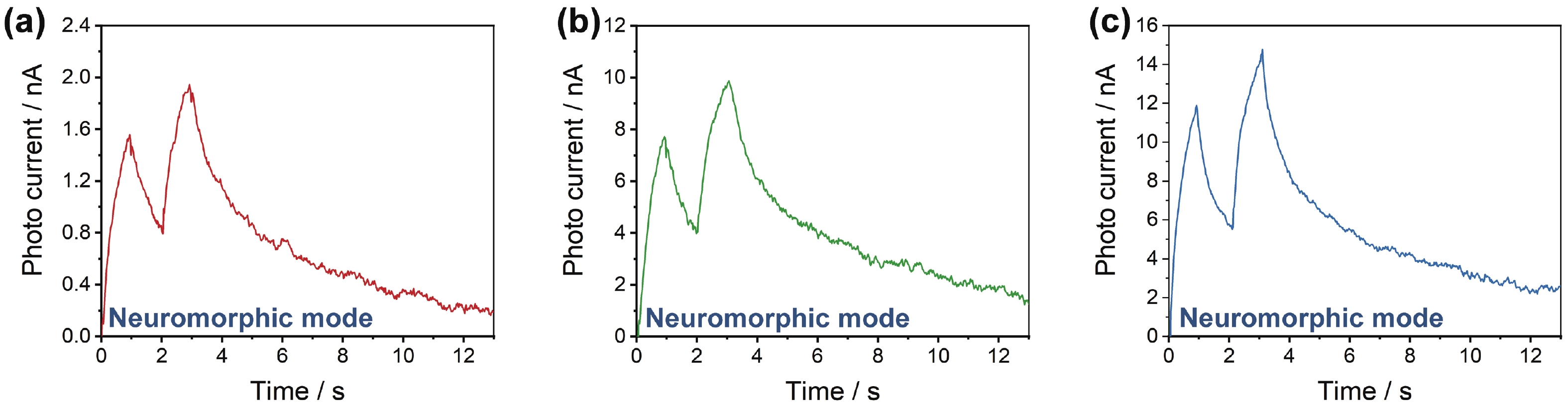
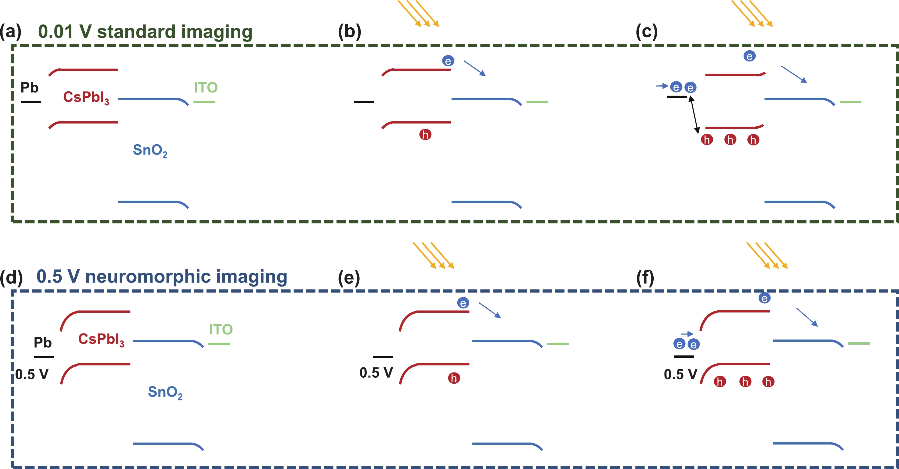
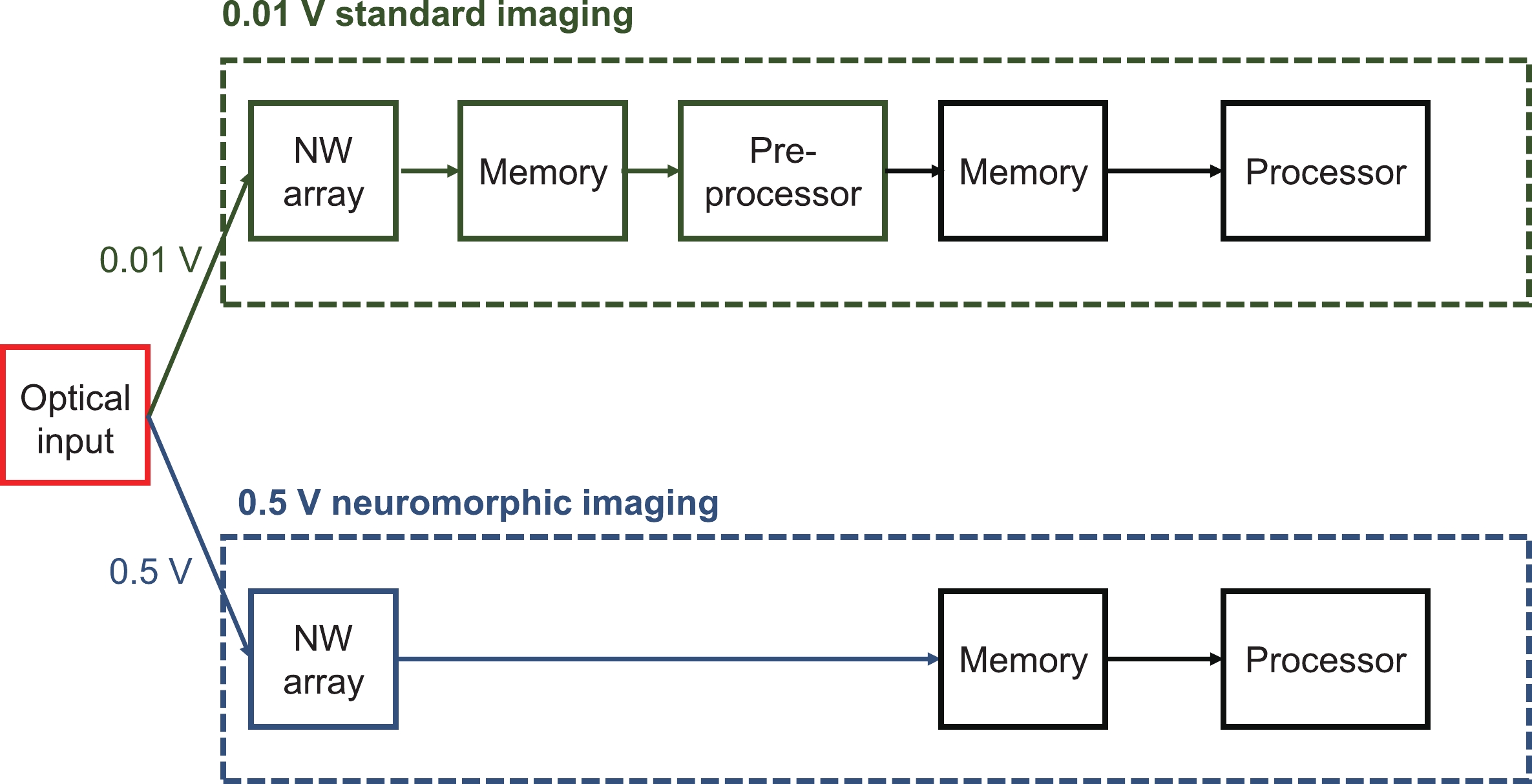
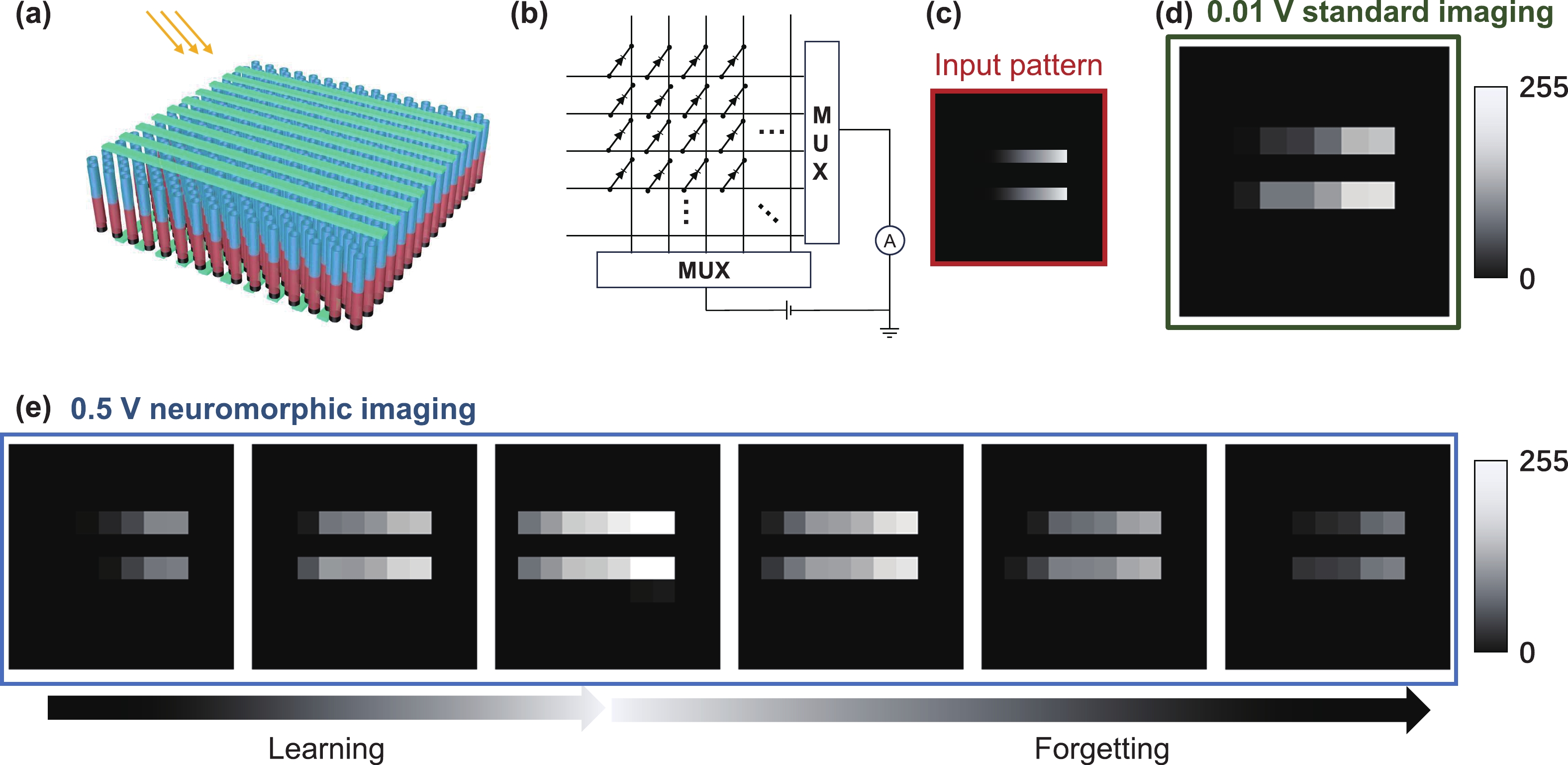
| [1] |
Wang S Y, Chen C S, Yu Z H, et al. A MoS 2/PTCDA hybrid heterojunction synapse with efficient photoelectric dual modulation and versatility. Adv Mater, 2019, 31, 1806227 doi: 10.1002/adma.201806227 |
| [2] |
He Y L, Nie S, Liu R, et al. Dual-functional long-term plasticity emulated in IGZO-based photoelectric neuromorphic transistors. IEEE Electron Device Lett, 2019, 40, 818 doi: 10.1109/LED.2019.2908727 |
| [3] |
Kumar M, Abbas S, Kim J. All-oxide-based highly transparent photonic synapse for neuromorphic computing. ACS Appl Mater Interfaces, 2018, 10, 34370 doi: 10.1021/acsami.8b10870 |
| [4] |
Pradhan B, Das S, Li J X, et al. Ultrasensitive and ultrathin phototransistors and photonic synapses using perovskite quantum dots grown from graphene lattice. Sci Adv, 2020, 6, eaay5225 doi: 10.1126/sciadv.aay5225 |
| [5] |
|
| [6] |
Mao J Y, Hu L, Zhang S R, et al. Artificial synapses emulated through a light mediated organic–inorganic hybrid transistor. J Mater Chem C, 2019, 7, 48 doi: 10.1039/C8TC05030A |
| [7] |
Zhang J Y, Dai S L, Zhao Y W, et al. Recent progress in photonic synapses for neuromorphic systems. Adv Intell Syst, 2020, 2, 1900136 doi: 10.1002/aisy.201900136 |
| [8] |
Han H, Yu H Y, Wei H H, et al. Three-terminal artificial synapses: Recent progress in three-terminal artificial synapses: From device to system (small 32/2019). Small, 2019, 15, 1900695 doi: 10.1002/smll.201900695 |
| [9] |
Zhou W, Yang R, He H K, et al. Optically modulated electric synapses realized with memristors based on ZnO nanorods. Appl Phys Lett, 2018, 113, 061107 doi: 10.1063/1.5045643 |
| [10] |
Zhou F C, Zhou Z, Chen J W, et al. Optoelectronic resistive random access memory for neuromorphic vision sensors. Nat Nanotechnol, 2019, 14, 776 doi: 10.1038/s41565-019-0501-3 |
| [11] |
Gu L L, Poddar S, Lin Y J, et al. A biomimetic eye with a hemispherical perovskite nanowire array retina. Nature, 2020, 581, 278 doi: 10.1038/s41586-020-2285-x |
| [12] |
Ding Y C, Liu G Z, Long Z H, et al. Uncooled self-powered hemispherical biomimetic pit organ for mid- to long-infrared imaging. Sci Adv, 2022, 8, eabq8432 doi: 10.1126/sciadv.abq8432 |
| [13] |
Long Z H, Qiu X, Chan C L J, et al. A neuromorphic bionic eye with filter-free color vision using hemispherical perovskite nanowire array retina. Nat Commun, 2023, 14, 1972 doi: 10.1038/s41467-023-37581-y |
| [14] |
Hu M Y, Chen M, Guo P J, et al. Sub-1.4eV bandgap inorganic perovskite solar cells with long-term stability. Nat Commun, 2020, 11, 151 doi: 10.1038/s41467-019-13908-6 |
| [15] |
Steele J A, Braeckevelt T, Prakasam V, et al. An embedded interfacial network stabilizes inorganic CsPbI 3 perovskite thin films. Nat Commun, 2022, 13, 7513 doi: 10.1038/s41467-022-35255-9 |
| [16] |
Tian T, Yang M F, Yang J Y, et al. Stabilizing black-phase CsPbI 3 under over 70% humidity. J Semicond, 2022, 43, 030501 doi: 10.1088/1674-4926/43/3/030501 |
| [17] |
Li Z Z, Jin Z W. HI hydrolysis-derived intermediate as booster for CsPbI 3 perovskite: From crystal structure, film fabrication to device performance. J Semicond, 2020, 41, 051202 doi: 10.1088/1674-4926/41/5/051202 |
| [18] |
Zhu Y Y, Shu L, Poddar S, et al. Three-dimensional nanopillar arrays-based efficient and flexible perovskite solar cells with enhanced stability. Nano Lett, 2022, 22, 9586 doi: 10.1021/acs.nanolett.2c03694 |
| [19] |
Xu X J, Li S Y, Chen J X, et al. Photodetectors: Design principles and material engineering of ZnS for optoelectronic devices and catalysis (adv. funct. mater. 36/2018). Adv Funct Materials, 2018, 28, 1802029 doi: 10.1002/adfm.201802029 |
| [20] |
Long Z H, Xu X J, Yang W, et al. Cross-bar SnO 2-NiO nanofiber-array-based transparent photodetectors with high detectivity. Adv Elect Materials, 2020, 6, 1901048 doi: 10.1002/aelm.201901048 |
| [21] |
Xu X J, Chen J X, Cai S, et al. Wearable health monitoring: A real-time wearable UV-radiation monitor based on a high-performance p-CuZnS/n-TiO 2 photodetector. Adv Mater, 2018, 30, 1803165 doi: 10.1002/adma.201803165 |
| [22] |
Zhou Y, Qiu X, Wan Z A, et al. Halide-exchanged perovskite photodetectors for wearable visible-blind ultraviolet monitoring. Nano Energy, 2022, 100, 107516 doi: 10.1016/j.nanoen.2022.107516 |
| [23] |
Leung S F, Gu L L, Zhang Q P, et al. Roll-to-roll fabrication of large scale and regular arrays of three-dimensional nanospikes for high efficiency and flexible photovoltaics. Sci Rep, 2014, 4, 4243 doi: 10.1038/srep04243 |
| [24] |
Yu R, Ching K L, Lin Q F, et al. Strong light absorption of self-organized 3-D nanospike arrays for photovoltaic applications. ACS Nano, 2011, 5, 9291 doi: 10.1021/nn203844z |
| [25] |
Gu L L, Zhang D Q, Kam M, et al. Significantly improved black phase stability of FAPbI 3 nanowires via spatially confined vapor phase growth in nanoporous templates. Nanoscale, 2018, 10, 15164 doi: 10.1039/C8NR03058H |
| [26] |
Li Z Q, Yan T T, Fang X S. Low-dimensional wide-bandgap semiconductors for UV photodetectors. Nat Rev Mater, 2023, 8, 587 doi: 10.1038/s41578-023-00583-9 |
| [27] |
Lin Y J, Chen J Q, Tavakoli M M, et al. Printable fabrication of a fully integrated and self-powered sensor system on plastic substrates. Adv Mater, 2019, 31, 1804285 doi: 10.1002/adma.201804285 |
| [28] |
Liang S Y, Liu Y F, Wang S Y, et al. High-resolution patterning of 2D perovskite films through femtosecond laser direct writing. Adv Funct Materials, 2022, 32, 0224957 doi: 10.1002/adfm.202204957 |
| [29] |
Lamers N, Zhang Z J, Wallentin J. Perovskite-compatible electron-beam-lithography process based on nonpolar solvents for single-nanowire devices. ACS Appl Nano Mater, 2022, 5, 3177 doi: 10.1021/acsanm.2c00188 |
| [30] |
van Breemen A J J M, Ollearo R, Shanmugam S, et al. A thin and flexible scanner for fingerprints and documents based on metal halide perovskites. Nat Electron, 2021, 4, 818 doi: 10.1038/s41928-021-00662-1 |


 DownLoad:


 Zhenghao Long:got his bachelor's degree in 2019 from Fudan University. Now he is a Ph.D. candidate at The Hong Kong University of Science and Technology under the supervision of Prof. Zhiyong Fan. His research focuses on nanomaterials and biomimetic optoelectronics
 Yucheng Ding:got his bachelor's degree in 2020 from Nanjing University. Now he is a Ph.D. candidate at The Hongkong University of Science and Technology under the supervision of Prof. Zhiyong Fan. His research focuses on optoelectronic devices based on nanostructures and novel materials
 Zhiyong Fan:is a Chair Professor at the Department of Electronic and Computer Engineering, The Hong Kong University of Science and Technology (HKUST). He received B.S. and M.S. degrees from Fudan University, Ph.D. degree from University of California, Irvine in 2006 then worked as a postdoctoral fellow at UC Berkeley and Lawrence Berkeley National Laboratory. Currently, he is the Co-director of the State Key Laboratory of Advanced Display and Optoelectronics Technologies at HKUST. He is a Fellow of the Royal Society of Chemistry, Fellow of Optica, Senior Member of IEEE, and Founding Member of the Young Academy of Sciences of Hong Kong. His research interest is focused on functional nanomaterials and structures for electronic, optoelectronic and bionic electronic devices


