


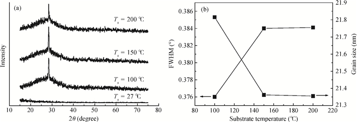
Fig. 1.
(a) XRD patterns of ZnS:In film. (b) FWHM/grain size variation with $T_{\rm s}$ .
SEMICONDUCTOR MATERIALS
Wenjian Li1, Jinhuo Chen1, , Shuying Cheng1 and Yongshun Wang2
Corresponding author: Chen Jinhuo, yeschen@fzu.edu.cn
Abstract: Indium doped ZnS (ZnS:In) films were prepared on glass substrate by using thermal evaporation technology. It was found that the structural, optical and electrical properties of ZnS:In films strongly depend on the substrate temperature (Ts). By utilizing X-ray diffraction (XRD), atomic force microscopy (AFM), transmittance spectroscopy, and electric performance measurements, the effect of Ts on ZnS:In film is studied in detail. It reveals that Ts has important effect on ZnS grain size, crystallinity, lattice disorder, etc., which further leads to the obvious influence on its optical and electrical performance. Under the optimized Ts, the performance, especially the conductivity, achieved in this work is far higher than that reported for other n-type ZnS films.
Keywords: ZnS, indium, evaporation, photoelectric properties, substrate temperature
| [1] |
Nagamani K, Prathap P. Properties of Al-doped ZnS films grown by chemical bath deposition. Physics Procedia, 2012, 25:137 doi: 10.1016/j.phpro.2012.03.062
|
| [2] |
Yu Z, Leng J, Xue W. Highly flexible transparent and conductive ZnS/Ag/ZnS multilayer films prepared by ion beam assisted deposition. Appl Surf Sci, 2012, 258:2270 doi: 10.1016/j.apsusc.2011.09.099
|
| [3] |
Yang P, Lu M, Xu D, et al. The photoluminescence characteristics of ZnS nanocrystal doped with M3+(M=In, Ga, Al). Mater Research Bulletin, 2001, 36:1301 doi: 10.1016/S0025-5408(01)00616-X
|
| [4] |
M A Contreras, T Nakada, M Hongo. ZnO/ZnS(O, OH)/Cu(In, Ga)Se2/Mo solar cell with 18. 6% efficiency. Proceedings of 3rd World Conference on of Photovoltaic Energy Conversion, Osaka, Japan, 2003, 1: 570
|
| [5] |
Gode F, Gumus C, Zor M. Investigations on the physical properties of the polycrystalline ZnS thin films deposited by the chemical bath deposition method. J Cryst Growth, 2007, 299:136 doi: 10.1016/j.jcrysgro.2006.10.266
|
| [6] |
Ashour A, Afifi H H, Mahmoud S A. Effect of some spray-pyrolysis parameters on electrical and optical-properties of ZnS films. Thin Solid Films, 1994, 248:253 doi: 10.1016/0040-6090(94)90020-5
|
| [7] |
Prathap P, Revath N, Subbaiah Y P V. Preparation and characterization of transparent conducting ZnS:Al films. Solid State Sci, 2009, 11:224 doi: 10.1016/j.solidstatesciences.2008.04.020
|
| [8] |
Anomalous B E. Optical absorption limit in InSb. Phys Rev, 1954, 93:632 doi: 10.1103/PhysRev.93.632
|


Article views: 3599 Times PDF downloads: 19 Times Cited by: 0 Times
Received: 01 July 2013 Revised: 25 August 2013 Online: Published: 01 February 2014
| Citation: |
Wenjian Li, Jinhuo Chen, Shuying Cheng, Yongshun Wang. Substrate temperature effects on the structural and photoelectric properties of ZnS:In films[J]. Journal of Semiconductors, 2014, 35(2): 023001. doi: 10.1088/1674-4926/35/2/023001
****
W J Li, J H Chen, S Y Cheng, Y S Wang. Substrate temperature effects on the structural and photoelectric properties of ZnS:In films[J]. J. Semicond., 2014, 35(2): 023001. doi: 10.1088/1674-4926/35/2/023001.

|
| [1] |
Nagamani K, Prathap P. Properties of Al-doped ZnS films grown by chemical bath deposition. Physics Procedia, 2012, 25:137 doi: 10.1016/j.phpro.2012.03.062
|
| [2] |
Yu Z, Leng J, Xue W. Highly flexible transparent and conductive ZnS/Ag/ZnS multilayer films prepared by ion beam assisted deposition. Appl Surf Sci, 2012, 258:2270 doi: 10.1016/j.apsusc.2011.09.099
|
| [3] |
Yang P, Lu M, Xu D, et al. The photoluminescence characteristics of ZnS nanocrystal doped with M3+(M=In, Ga, Al). Mater Research Bulletin, 2001, 36:1301 doi: 10.1016/S0025-5408(01)00616-X
|
| [4] |
M A Contreras, T Nakada, M Hongo. ZnO/ZnS(O, OH)/Cu(In, Ga)Se2/Mo solar cell with 18. 6% efficiency. Proceedings of 3rd World Conference on of Photovoltaic Energy Conversion, Osaka, Japan, 2003, 1: 570
|
| [5] |
Gode F, Gumus C, Zor M. Investigations on the physical properties of the polycrystalline ZnS thin films deposited by the chemical bath deposition method. J Cryst Growth, 2007, 299:136 doi: 10.1016/j.jcrysgro.2006.10.266
|
| [6] |
Ashour A, Afifi H H, Mahmoud S A. Effect of some spray-pyrolysis parameters on electrical and optical-properties of ZnS films. Thin Solid Films, 1994, 248:253 doi: 10.1016/0040-6090(94)90020-5
|
| [7] |
Prathap P, Revath N, Subbaiah Y P V. Preparation and characterization of transparent conducting ZnS:Al films. Solid State Sci, 2009, 11:224 doi: 10.1016/j.solidstatesciences.2008.04.020
|
| [8] |
Anomalous B E. Optical absorption limit in InSb. Phys Rev, 1954, 93:632 doi: 10.1103/PhysRev.93.632
|

 WeChat ID
Journal of Semiconductors © 2017 All Rights Reserved 京ICP备05085259号-2

 DownLoad:

