Fig. 1.
NF distribution of the dual-band receiver with passive or active antenna.
SEMICONDUCTOR INTEGRATED CIRCUITS
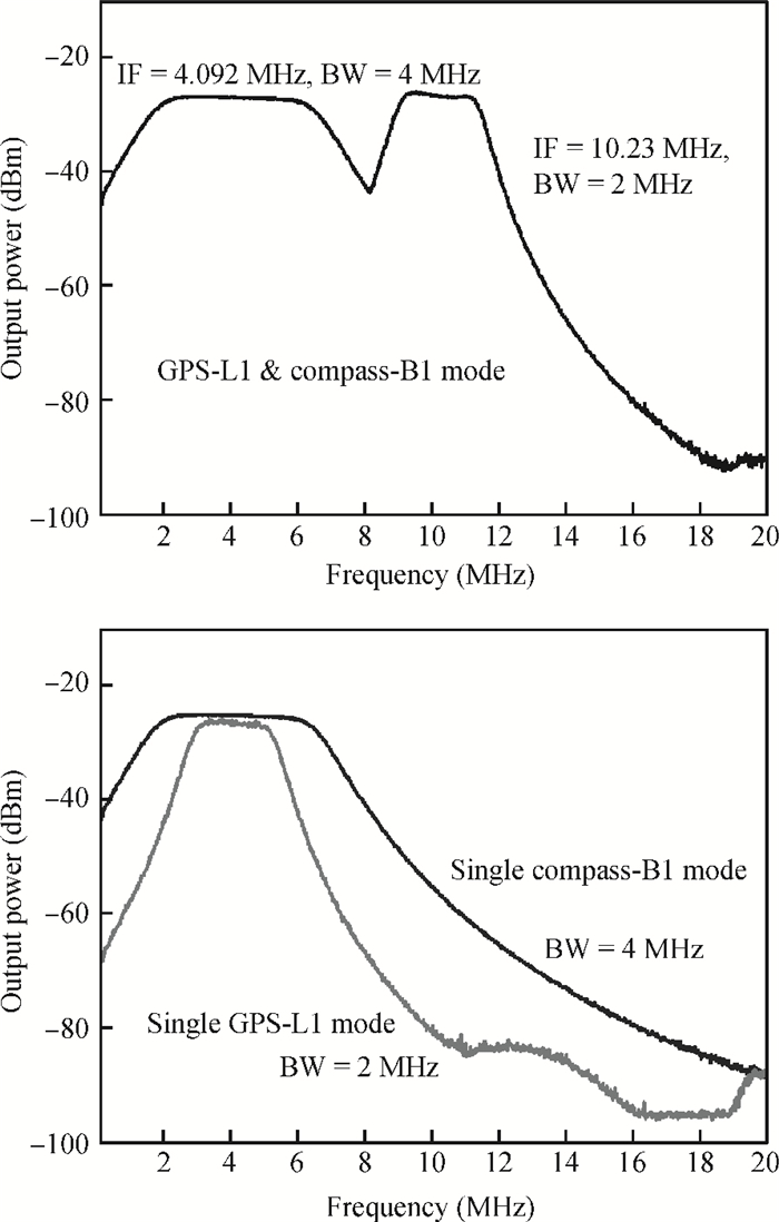
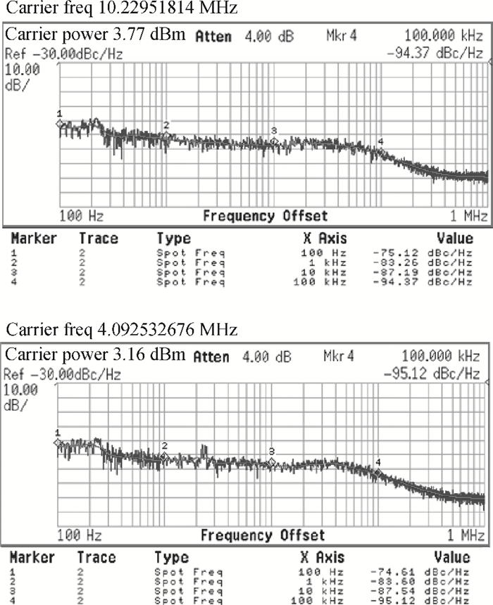
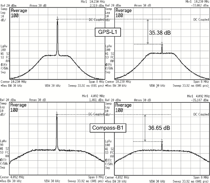
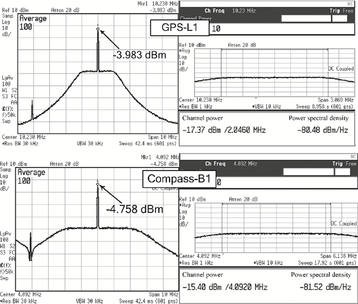
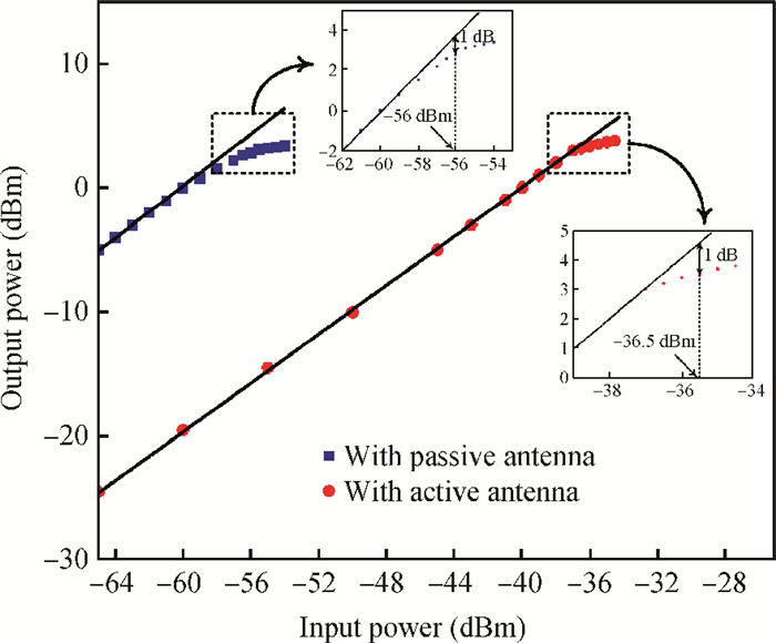
Abstract: A fully integrated dual-band RF receiver with a low-IF architecture is designed and implemented for GPS-L1 and Compass-B1 in a 55-nm CMOS process. The receiver incorporates two independent IF channels with 2 or 4 MHz bandwidth to receive dual-band signals around 1.57 GHz respectively. By implementing a flexible frequency plan, the RF front-end and frequency synthesizer are shared for the dual-band operation to save power consumption and chip area, as well as avoiding LO crosstalk. A digital automatic gain control (AGC) loop is utilized to improve the receiver's robustness by optimizing the conversion gain of the analog-to-digital converter (ADC). While drawing about 20 mA per channel from a 1.2 V supply, this RF receiver achieves a minimum noise figure (NF) of about 1.8 dB, an image rejection (IMR) of more than 35 dB, a maximum voltage gain of about 122 dB, a gain dynamic range of 82 dB, and an maximum input-referred 1 dB compression point of about -36.5 dBm with an active die area of 1.5×1.4 mm2 for the whole chip.
Keywords: automatic gain control, CMOS, compass, dual-band, GPS, RF receiver
| [1] |
Prades C, Presti L, Falletti E. Satellite radio localization form GPS to GNSS and beyond:novel technologies and applications for civil mass market. Proc IEEE, 2011, 99:1882 doi: 10.1109/JPROC.2011.2158032
|
| [2] |
Detratti M, Lopez E, Perez E R, et al. Dual-band RF receiver chip-set for Galileo/GPS applications. IEEE Position, Location and Navigation Symp, 2008:851 http://ieeexplore.ieee.org/document/4569991/authors
|
| [3] |
Pizzarulli A, Montagna G, Pini M, et al. Reconfigurable and simultaneous dual band Galileo/GPS front-end receiver in 0.13μm RFCMOS. IEEE Position, Location and Navigation Symp, 2008:846 http://ieeexplore.ieee.org/document/4569990/?arnumber=4569990&contentType=Conference+Publications
|
| [4] |
Moon Y, Cha S, Kim G. A 26 mW dual-mode RF receiver for GPS/Galileo with L1/L1F and L5/E5a bands. IEEE Int SoC Design Conf, 2008:Ⅰ-421 doi: 10.1088/1674-4926/35/2/025001/meta
|
| [5] |
Wistuba G, Vasylyev A, Haas S, et al. A highly integrated configurable GNSS receiver frontend design for high bandwidth operation on E1/L1 and E5a/L5. Int Conf on Localization and GNSS, 2011:164 doi: 10.1088/1674-4926/35/2/025001/meta
|
| [6] |
Jo J, Lee J, Park D, et al. An L1-band dual-mode RF receiver for GPS and Galileo in 0.18-μm CMOS. IEEE Trans Microw Theory Tech, 2009, 57:919 doi: 10.1109/TMTT.2009.2014432
|
| [7] |
Qi N, Xu Y, Chi B, et al. A dual-channel Compass/GPS/GLONASS/Galileo reconfigurable GNSS receiver in 65 nm CMOS with on-chip I/Q calibration. IEEE Trans Circuits Syst I, Reg Papers, 2012, 59:1720 doi: 10.1109/TCSI.2012.2206502
|
| [8] |
Chen D, Pan W, Jiang P, et al. Reconfigurable dual-channel multiband RF receiver for GPS/Galileo/BD-2 systems. IEEE Trans Microw Theory Tech, 2012, 60:3491 doi: 10.1109/TMTT.2012.2216287
|
| [9] |
Tan C, Song F, Choke T, et al. A universal GNSS (GPS/Galileo/Glonass/BeiDou) SoC with a 0.25 mm2 radio in 40 nm CMOS. IEEE Int Solid-State Circ Conf, Tech Dig, 2013:334 doi: 10.1088/1674-4926/35/2/025001/meta
|
| [10] |
Sun F, Liu S, Zhu X, et al. Research and progress of Beidou satellite navigation system. Science China:Information Sciences, 2012, 55:2899 doi: 10.1007/s11432-012-4724-2
|
| [11] |
Ko J, Kim J, Cho S, et al. A 19-mW 2.6-mm2 L1/L2 dual-band CMOS GPS receiver. IEEE J Solid-State Circuits, 2005, 40:1414 doi: 10.1109/JSSC.2005.847326
|
| [12] |
Amoroso F. Adaptive A/D converter to suppress CW interference in DSPN spread-spectrum communications. IEEE Trans Commun, 1983, COM-31:1117 http://ieeexplore.ieee.org/document/4794795/?reload=true&arnumber=4794795&punumber%3D4794639
|
| [13] |
Nguyen T, Oh N, Le V, et al. A low-power CMOS direct conversion receiver with 3-dB NF and 30-kHz flicker-noise corner for 915-MHz band IEEE 802.15.4 ZigBee standard. IEEE Trans Microw Theory Tech, 2006, 54:735 doi: 10.1109/TMTT.2005.862636
|
| [14] |
Chen D, Yan T, Jin J, et al. A tri-mode Compass/GPS/Galileo RF receiver with all-digital automatic gain control loop. Analog Integr Circ Sig Process, 2011, 70:69 doi: 10.1007/s10470-011-9656-z?no-access=true
|
| [15] |
Amoroso F, Bricker J. Performance of the adaptive A/D converter in combined CW and Gaussian interference. IEEE Trans Commun, 1986, COM-34:209 doi: 10.1109/TCOM.1986.1096517
|
| [16] |
Moon H, Lee S, Heo S, et al. A 23 mW fully integrated GPS receiver with robust interferer rejection in 65 nm CMOS. IEEE Int Solid-State Circ Conf, Tech Dig, 2010:68 http://ieeexplore.ieee.org/document/5434047/?reload=true&arnumber=5434047&contentType=Conference+Publications
|
Table 1. Operating modes and frequency plan of the dual-band receiver (Unit: MHz).

|
Table 2. Distribution of the gain ranges and steps for PGA.

|
Table 3. Performance summary and comparison to other state-of-the-art devices.

|
| [1] |
Prades C, Presti L, Falletti E. Satellite radio localization form GPS to GNSS and beyond:novel technologies and applications for civil mass market. Proc IEEE, 2011, 99:1882 doi: 10.1109/JPROC.2011.2158032
|
| [2] |
Detratti M, Lopez E, Perez E R, et al. Dual-band RF receiver chip-set for Galileo/GPS applications. IEEE Position, Location and Navigation Symp, 2008:851 http://ieeexplore.ieee.org/document/4569991/authors
|
| [3] |
Pizzarulli A, Montagna G, Pini M, et al. Reconfigurable and simultaneous dual band Galileo/GPS front-end receiver in 0.13μm RFCMOS. IEEE Position, Location and Navigation Symp, 2008:846 http://ieeexplore.ieee.org/document/4569990/?arnumber=4569990&contentType=Conference+Publications
|
| [4] |
Moon Y, Cha S, Kim G. A 26 mW dual-mode RF receiver for GPS/Galileo with L1/L1F and L5/E5a bands. IEEE Int SoC Design Conf, 2008:Ⅰ-421 doi: 10.1088/1674-4926/35/2/025001/meta
|
| [5] |
Wistuba G, Vasylyev A, Haas S, et al. A highly integrated configurable GNSS receiver frontend design for high bandwidth operation on E1/L1 and E5a/L5. Int Conf on Localization and GNSS, 2011:164 doi: 10.1088/1674-4926/35/2/025001/meta
|
| [6] |
Jo J, Lee J, Park D, et al. An L1-band dual-mode RF receiver for GPS and Galileo in 0.18-μm CMOS. IEEE Trans Microw Theory Tech, 2009, 57:919 doi: 10.1109/TMTT.2009.2014432
|
| [7] |
Qi N, Xu Y, Chi B, et al. A dual-channel Compass/GPS/GLONASS/Galileo reconfigurable GNSS receiver in 65 nm CMOS with on-chip I/Q calibration. IEEE Trans Circuits Syst I, Reg Papers, 2012, 59:1720 doi: 10.1109/TCSI.2012.2206502
|
| [8] |
Chen D, Pan W, Jiang P, et al. Reconfigurable dual-channel multiband RF receiver for GPS/Galileo/BD-2 systems. IEEE Trans Microw Theory Tech, 2012, 60:3491 doi: 10.1109/TMTT.2012.2216287
|
| [9] |
Tan C, Song F, Choke T, et al. A universal GNSS (GPS/Galileo/Glonass/BeiDou) SoC with a 0.25 mm2 radio in 40 nm CMOS. IEEE Int Solid-State Circ Conf, Tech Dig, 2013:334 doi: 10.1088/1674-4926/35/2/025001/meta
|
| [10] |
Sun F, Liu S, Zhu X, et al. Research and progress of Beidou satellite navigation system. Science China:Information Sciences, 2012, 55:2899 doi: 10.1007/s11432-012-4724-2
|
| [11] |
Ko J, Kim J, Cho S, et al. A 19-mW 2.6-mm2 L1/L2 dual-band CMOS GPS receiver. IEEE J Solid-State Circuits, 2005, 40:1414 doi: 10.1109/JSSC.2005.847326
|
| [12] |
Amoroso F. Adaptive A/D converter to suppress CW interference in DSPN spread-spectrum communications. IEEE Trans Commun, 1983, COM-31:1117 http://ieeexplore.ieee.org/document/4794795/?reload=true&arnumber=4794795&punumber%3D4794639
|
| [13] |
Nguyen T, Oh N, Le V, et al. A low-power CMOS direct conversion receiver with 3-dB NF and 30-kHz flicker-noise corner for 915-MHz band IEEE 802.15.4 ZigBee standard. IEEE Trans Microw Theory Tech, 2006, 54:735 doi: 10.1109/TMTT.2005.862636
|
| [14] |
Chen D, Yan T, Jin J, et al. A tri-mode Compass/GPS/Galileo RF receiver with all-digital automatic gain control loop. Analog Integr Circ Sig Process, 2011, 70:69 doi: 10.1007/s10470-011-9656-z?no-access=true
|
| [15] |
Amoroso F, Bricker J. Performance of the adaptive A/D converter in combined CW and Gaussian interference. IEEE Trans Commun, 1986, COM-34:209 doi: 10.1109/TCOM.1986.1096517
|
| [16] |
Moon H, Lee S, Heo S, et al. A 23 mW fully integrated GPS receiver with robust interferer rejection in 65 nm CMOS. IEEE Int Solid-State Circ Conf, Tech Dig, 2010:68 http://ieeexplore.ieee.org/document/5434047/?reload=true&arnumber=5434047&contentType=Conference+Publications
|


Article views: 3564 Times PDF downloads: 45 Times Cited by: 0 Times
Received: 05 July 2013 Revised: 13 August 2013 Online: Published: 01 February 2014
| Citation: |
Songting Li, Jiancheng Li, Xiaochen Gu, Zhaowen Zhuang. Dual-band RF receiver for GPS-L1 and compass-B1 in a 55-nm CMOS[J]. Journal of Semiconductors, 2014, 35(2): 025001. doi: 10.1088/1674-4926/35/2/025001
****
S T Li, J C Li, X C Gu, Z W Zhuang. Dual-band RF receiver for GPS-L1 and compass-B1 in a 55-nm CMOS[J]. J. Semicond., 2014, 35(2): 025001. doi: 10.1088/1674-4926/35/2/025001.

|
| [1] |
Prades C, Presti L, Falletti E. Satellite radio localization form GPS to GNSS and beyond:novel technologies and applications for civil mass market. Proc IEEE, 2011, 99:1882 doi: 10.1109/JPROC.2011.2158032
|
| [2] |
Detratti M, Lopez E, Perez E R, et al. Dual-band RF receiver chip-set for Galileo/GPS applications. IEEE Position, Location and Navigation Symp, 2008:851 http://ieeexplore.ieee.org/document/4569991/authors
|
| [3] |
Pizzarulli A, Montagna G, Pini M, et al. Reconfigurable and simultaneous dual band Galileo/GPS front-end receiver in 0.13μm RFCMOS. IEEE Position, Location and Navigation Symp, 2008:846 http://ieeexplore.ieee.org/document/4569990/?arnumber=4569990&contentType=Conference+Publications
|
| [4] |
Moon Y, Cha S, Kim G. A 26 mW dual-mode RF receiver for GPS/Galileo with L1/L1F and L5/E5a bands. IEEE Int SoC Design Conf, 2008:Ⅰ-421 doi: 10.1088/1674-4926/35/2/025001/meta
|
| [5] |
Wistuba G, Vasylyev A, Haas S, et al. A highly integrated configurable GNSS receiver frontend design for high bandwidth operation on E1/L1 and E5a/L5. Int Conf on Localization and GNSS, 2011:164 doi: 10.1088/1674-4926/35/2/025001/meta
|
| [6] |
Jo J, Lee J, Park D, et al. An L1-band dual-mode RF receiver for GPS and Galileo in 0.18-μm CMOS. IEEE Trans Microw Theory Tech, 2009, 57:919 doi: 10.1109/TMTT.2009.2014432
|
| [7] |
Qi N, Xu Y, Chi B, et al. A dual-channel Compass/GPS/GLONASS/Galileo reconfigurable GNSS receiver in 65 nm CMOS with on-chip I/Q calibration. IEEE Trans Circuits Syst I, Reg Papers, 2012, 59:1720 doi: 10.1109/TCSI.2012.2206502
|
| [8] |
Chen D, Pan W, Jiang P, et al. Reconfigurable dual-channel multiband RF receiver for GPS/Galileo/BD-2 systems. IEEE Trans Microw Theory Tech, 2012, 60:3491 doi: 10.1109/TMTT.2012.2216287
|
| [9] |
Tan C, Song F, Choke T, et al. A universal GNSS (GPS/Galileo/Glonass/BeiDou) SoC with a 0.25 mm2 radio in 40 nm CMOS. IEEE Int Solid-State Circ Conf, Tech Dig, 2013:334 doi: 10.1088/1674-4926/35/2/025001/meta
|
| [10] |
Sun F, Liu S, Zhu X, et al. Research and progress of Beidou satellite navigation system. Science China:Information Sciences, 2012, 55:2899 doi: 10.1007/s11432-012-4724-2
|
| [11] |
Ko J, Kim J, Cho S, et al. A 19-mW 2.6-mm2 L1/L2 dual-band CMOS GPS receiver. IEEE J Solid-State Circuits, 2005, 40:1414 doi: 10.1109/JSSC.2005.847326
|
| [12] |
Amoroso F. Adaptive A/D converter to suppress CW interference in DSPN spread-spectrum communications. IEEE Trans Commun, 1983, COM-31:1117 http://ieeexplore.ieee.org/document/4794795/?reload=true&arnumber=4794795&punumber%3D4794639
|
| [13] |
Nguyen T, Oh N, Le V, et al. A low-power CMOS direct conversion receiver with 3-dB NF and 30-kHz flicker-noise corner for 915-MHz band IEEE 802.15.4 ZigBee standard. IEEE Trans Microw Theory Tech, 2006, 54:735 doi: 10.1109/TMTT.2005.862636
|
| [14] |
Chen D, Yan T, Jin J, et al. A tri-mode Compass/GPS/Galileo RF receiver with all-digital automatic gain control loop. Analog Integr Circ Sig Process, 2011, 70:69 doi: 10.1007/s10470-011-9656-z?no-access=true
|
| [15] |
Amoroso F, Bricker J. Performance of the adaptive A/D converter in combined CW and Gaussian interference. IEEE Trans Commun, 1986, COM-34:209 doi: 10.1109/TCOM.1986.1096517
|
| [16] |
Moon H, Lee S, Heo S, et al. A 23 mW fully integrated GPS receiver with robust interferer rejection in 65 nm CMOS. IEEE Int Solid-State Circ Conf, Tech Dig, 2010:68 http://ieeexplore.ieee.org/document/5434047/?reload=true&arnumber=5434047&contentType=Conference+Publications
|

 WeChat ID
Journal of Semiconductors © 2017 All Rights Reserved 京ICP备05085259号-2

 DownLoad: