.
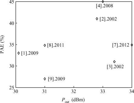
Comparison of watt-level output power CMOS PAs.
SEMICONDUCTOR INTEGRATED CIRCUITS
Zhixiong Ren, Kefeng Zhang, Lanqi Liu, Cong Li, Xiaofei Chen, Dongsheng Liu, Zhenglin Liu and Xuecheng Zou
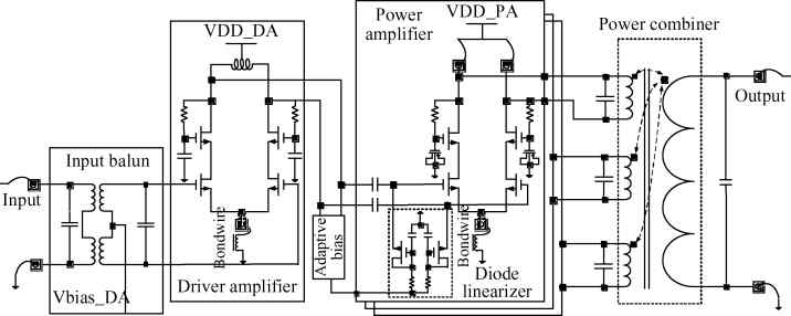
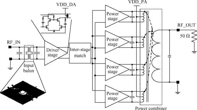
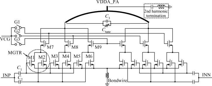
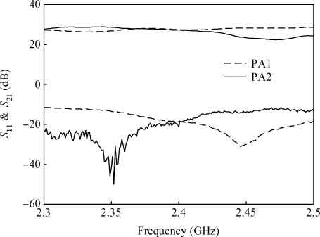
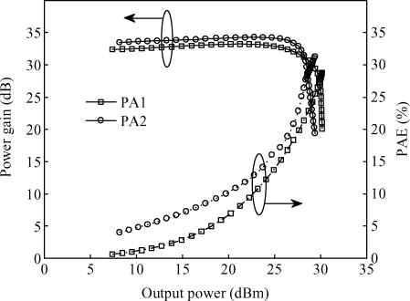
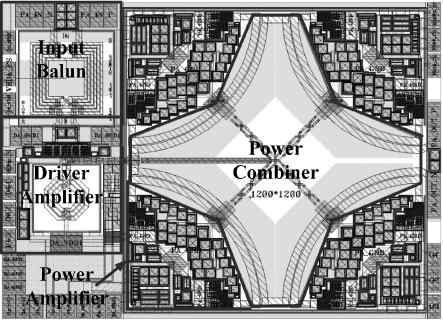
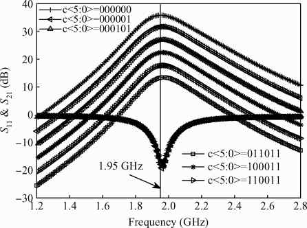
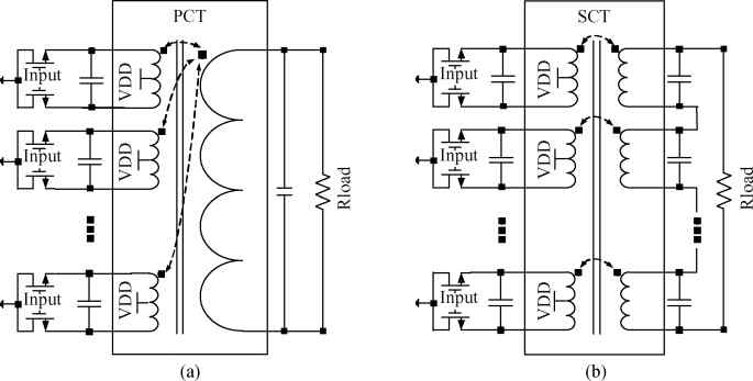
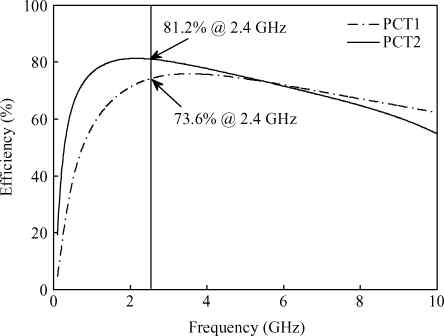
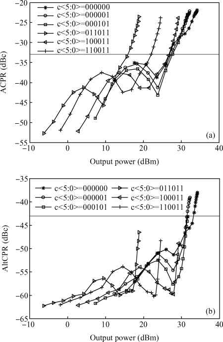
Abstract: Three linear CMOS power amplifiers (PAs) with high output power (more than watt-level output power) for high data-rate mobile applications are introduced. To realize watt-level output power, there are two 2.4 GHz PAs using an on-chip parallel combining transformer (PCT) and one 1.95 GHz PA using an on-chip series combining transformer (SCT) to combine output signals of multiple power stages. Furthermore, some linearization techniques including adaptive bias, diode linearizer, multi-gated transistors (MGTR) and the second harmonic control are applied in these PAs. Using the proposed power combiner, these three PAs are designed and fabricated in TSMC 0.18 μm RFCMOS process. According to the measurement results, the proposed two linear 2.4 GHz PAs achieve a gain of 33.2 dB and 34.3 dB, a maximum output power of 30.7 dBm and 29.4 dBm, with 29% and 31.3% of peak PAE, respectively. According to the simulation results, the presented linear 1.95 GHz PA achieves a gain of 37.5 dB, a maximum output power of 34.3 dBm with 36.3% of peak PAE.
Keywords: CMOS, linearity, power combiner, transformers, power amplifier
| [1] | |
| [2] | |
| [3] | |
| [4] | |
| [5] | |
| [6] | |
| [7] | |
| [8] | |
| [9] | |
| [10] | |
| [11] | |
| [12] | |
| [13] | |
| [14] | |
| [15] | |
| [16] | |
| [17] | |
| [18] | |
| [19] | |
| [20] | |
| [21] | |
| [22] | |
| [23] | |
| [24] | |
| [25] | |
| [26] | |
| [27] | |
| [28] | |
| [29] |


Article views: 4110 Times PDF downloads: 59 Times Cited by: 0 Times
Received: 03 March 2015 Revised: Online: Published: 01 September 2015
| Citation: |
Zhixiong Ren, Kefeng Zhang, Lanqi Liu, Cong Li, Xiaofei Chen, Dongsheng Liu, Zhenglin Liu, Xuecheng Zou. On-chip power-combining techniques for watt-level linear power amplifiers in 0.18 μm CMOS[J]. Journal of Semiconductors, 2015, 36(9): 095002. doi: 10.1088/1674-4926/36/9/095002
****
Z X Ren, K F Zhang, L Q Liu, C Li, X F Chen, D S Liu, Z L Liu, X C Zou. On-chip power-combining techniques for watt-level linear power amplifiers in 0.18 μm CMOS[J]. J. Semicond., 2015, 36(9): 095002. doi: 10.1088/1674-4926/36/9/095002.

|
| [1] | |
| [2] | |
| [3] | |
| [4] | |
| [5] | |
| [6] | |
| [7] | |
| [8] | |
| [9] | |
| [10] | |
| [11] | |
| [12] | |
| [13] | |
| [14] | |
| [15] | |
| [16] | |
| [17] | |
| [18] | |
| [19] | |
| [20] | |
| [21] | |
| [22] | |
| [23] | |
| [24] | |
| [25] | |
| [26] | |
| [27] | |
| [28] | |
| [29] |

 WeChat ID
Journal of Semiconductors © 2017 All Rights Reserved 京ICP备05085259号-2

 DownLoad: