1. Introduction
Currently in VLSI technology, circuit designs are based on CMOS technology. Advancement in the field is greatly driven by Moore's law, which predicts that every 18 months the functionality on a given chip area will be doubled[1] which means that device density has to double every 18 months. Until now CMOS technology has been able to hold to Moore's law. In order to do so, scaling of CMOS devices has been progressing at tremendous rate. But now the device sizes are reaching a limit, where further scaling of the device leads to various operational as well as fabrication complexities. According to the International Technology Roadmap for Semiconductors (ITRS 2013), further scaling of CMOS devices after 2025, when the device size (half pitch length) will already have reached 10 nm, will not be possible[2].
So there is a serious need to find an alternative to CMOS. Various studies are ongoing in the field of nanotechnology to come up with a technology which can replace the current CMOS technology. In Reference [2], some of the potential candidates for this have been identified. Quantum dot cellular automata (QCA) are one of them. A device paradigm based on QCA cells offers the opportunity to break away from FET based logic and to exploit the quantum effects that come with nano scale size.
The concept of QCA for computation was proposed by Lent in 1993 and the first QCA cell was fabricated in 1997 using aluminum islands and aluminum-oxide tunnel junctions on an oxidized silicon wafer using the standard electron beam lithography and dual shadow evaporation methods[3, 4]. This first QCA cell was operable at the very low cryogenic temperature of 70 mK. Semiconductor quantum dot fabrication yield is low and the additional energy typically differs for each additional electron, and the electrical behavior of the dot can change from run to run, making it difficult to prepare the cell for proper operation. This makes the metal dot an attractive option for QCA experiments, as it has a very high yield and is electrically well-behaved, but the main disadvantages of metal dot QCA are the background charge fluctuations and low operating temperature. After successful demonstration of fabricated QCA cells, researchers from Notre Dame and other intuitions have fabricated and verified majority gates, inverters, simple wires and shift registers[5, 6, 7]. They are all only operable at cryogenic temperatures, but with very high speed and negligible power dissipation and of course occupy a much smaller area compared to CMOS technology. Research is still ongoing to increase the operation temperature and bring it to room temperature. Since QCA cells are scalable to molecular dimensions and since the performance improves as the size shrinks, a molecular QCA cell should operate at room temperature. Since the fabrication of QCA devices is still in its nascent stage, the cost of large scale fabrication of QCA devices cannot be estimated and compared with the well developed CMOS technology.
CMOS devices basically act like current switches and information is encoded in the form of voltage levels at different nodes[8]. In QCA technology, information is encoded in the form of polarization state and information is transmitted through Columbic interaction[9]. Unlike CMOS, where computation (the logic gates) and information transmission (the wire) are handled separately; in QCA computation and communication occur side-by-side[10].
Much work has recently been undertaken in the field of circuit design in QCA. The first 1-bit full adder in QCA was proposed by Tougaw and Lent in 1994[11]. The design of adders is one of the most studied topics in circuit design in QCA technology[11, 12, 13, 14, 15].
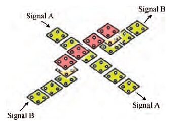
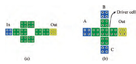
Although wire crossing in QCA is one of the remarkable achievements in digital design, the specific nature of the QCA cell may introduce cross talk between two wires, due to Coulombic interaction between them. This wire crossing can be realized by either coplanar crossover in which each section is loosely coupled with another section of horizontal wire or with multilayered wires which are more robust than coplanar crossings because intermediate layers are used to prevent any possible cross talk. Unlike CMOS technology where only base layer is the active layer, in QCA technology each layer can be used as an active layer on which a circuit can be designed, but until now all the circuits reported in the literature have been designed in a single layer except for the multilayer wire crossing[13, 14]. In the case of multilayer wire crossing, information is transmitted through another layer over the main layer. In this methodology, cells are placed one above another in the vertical direction. In the top layer, data can again flow in a horizontal wire. Again, using cells which are placed one below another in the vertical direction, information is brought back in the main layer[16]. An illustration is shown in Figure 1.
Inspired by the concept of multilayer wire crossing, this paper proposes a novel design paradigm in QCA technology, in which the logic gates are also designed in the multilayer. The proposed design paradigm utilizes the inbuilt property of QCA technology: "logic computation and data transfer can take place through the same QCA cells, depending upon their relative arrangement". As in the proposed multilayer gate design paradigm, a gate does not need to be in a plane, one can shift the gate itself in three-dimensional space, rather than crossing over the wire, hence reducing the length of connecting wire, which makes the circuit more compact, reducing the requirement for QCA cells and improving input-output delays.
2. An overview of QCA
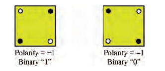
In QCA technology, binary information is stored in the form of bi-stable charge configurations of a QCA cell, rather than voltage levels as in CMOS technology. A QCA cell can be viewed as a set of four charge containers or dots, positioned at the corners of a square and it contains two extra mobile electrons which can quantum mechanically tunnel between the dots but not the cell. When excited, these two electrons, due to Coulombic repulsion, will occupy antipodal sites. Hence, there are two possible configurations. In Figure 2, both the states are energetically degenerated. But in the presence of any external electrostatic excitation, maybe due to another QCA cell in the neighborhood, the two polarization states become non-degenerated (Figure 3). The polarization state with lower energy will be the ground state of the QCA cell and the cell will polarize to the ground state[17]. This results in a technology in which information transfer (interconnection) is the same as information transformation (logic manipulation). In terms of feature size, it is projected that a QCA cell a few nanometers in size can be fabricated through molecular implementation using a self-assembly process.
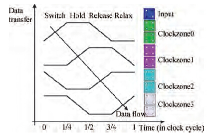
2.1 QCA clocking and input-output delay
In CMOS technology, the clock has two phases: high and low. But in QCA technology, the clock has four phases, switch, hold, release and relax, which are phase shifted by 90∘[18]. Clocking in QCA technology also determines the direction of information flow and power up in the QCA circuits[4, 19]. QCA cells are timed in four clocking zones phase shifted by 90∘. Logic computation takes place in the switch phase. In the hold phase the computed state is held, which acts as the input to the QCA cells in the subsequent clocking zones, which are in switch phase and ready for logic computation. In Figure 4, consider the time instance between a 1/4 clock cycle and a 1/2 clock cycle. During this time period, "Clockzone-0" is in the hold phase and "Clockzone-1" is in the switch phase. Logic computed in Clockzone-0 during its switch phase (0-1/4 clock cycle) will now be inputted to Clockzone-1 during the hold phase (1/4-1/2 clock cycle). It can be visualized from Figure~4 that information from the input cell will reach Clockzone-3 after a delay of 3/4 of a clock cycle (the number of clocking zones in between multiplied by 1/4 of a clock cycle).

2.2 Logic gates in QCA
The inverter and majority voter are the fundamental building blocks of any QCA circuit. The output of a majority gate is the polarization state, which is in majority in the inputs. So the output will be "1" only if two or all three inputs are "1". Designs for the inverter and majority gate are shown in Figures~5(a) and 5(b), respectively.
A reduced gate (AND/OR) can be obtained from the majority gate by fixing the polarity of one of its inputs. If we fix one of the inputs of the 3-input majority gate to "0", then for the output to be 1, the rest of the variable inputs have to be 1. This is the characteristic of the AND gate. In a similar fashion, it can be reasoned that, by fixing one of the inputs to 1, one can obtain a 2-input OR gate.
3. Fundamentals of the multilayer gate design technique
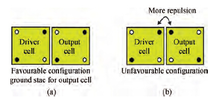
In a two cell system in a single layer, electrons rearrange themselves so as to minimize the Columbic repulsion. The state with minimum repulsion will be the ground state for the output cell (see Figure 3). The output cell will polarize to its ground state. In the multilayer the same principle also drives the output cell's polarization. When QCA cells are stacked one over another, electrons will rearrange themselves so as to minimize the Columbic repulsion. The state with minimum repulsion is the ground state and the output cell will polarize to its ground state. Intercellular Columbic interaction in a multilayer is shown in Figure 6.
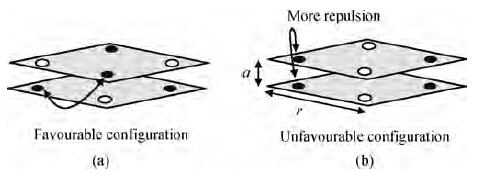
One can see from Figure 6(a) that the distance between the nearest electrons in two cells is (a+r)1/2 which is greater than "a" as in Figure 6(b). As the distance in Figure 6(a) is greater than in Figure 6(b), there will be less Coulombic repulsion in Figure 6(a) than that in Figure 6(b). Hence the configuration shown in Figure 6(a) is the ground state of the cells. In the ground state, cells will have opposite polarizations to each other. If we design a vertical wire out of the cells, we will obtain an inverter chain. Depending upon the location of the output from the inverter chain, one can obtain original as well as complementary data.
4. Logic gates in the multilayer gate design paradigm
In this section, a basic understanding of the layouts and operations of fundamental QCA logic devices in the multilayer gate design paradigm is provided.
4.1 The inverter
From Figure 6, it is evident that a stack of QCA cells act like an inverter chain. So, an inverter is already built in to the multilayer gate design paradigm. Two cells, one over another, in consecutive layers will act as an inverter.
4.2 The 3-input majority gate
Unlike a single layer, which has a fixed design for the majority gate, in a multilayer, due to the availability of an additional spatial dimension, one can come up with many innovative designs for the majority gate (any logic block for that matter). For majority gate design, a designer only has to keep two points in mind. The first being that an array of cells in the same layer will have the same polarity (a binary wire). Cells stacked over one another in two consecutive layers will have opposite polarity (an inverter chain). The second point to remember is that all the input cells of the majority gate should be placed such that they have an equal influence on the driver cell. Two designs for the 3-input majority gate are proposed in Figure 7.
The majority gate in Figure 7(a) uses eight QCA cells and is spread over five layers. Inputs B and C are two layers away from the driver cell. So a signal from them will reach the driver cell after two inversions. Hence both of these inputs will try to polarize the driver cell to match their polarity. Input A is in the same layer as the driver cell and both are in an array. So A will also try to force the driver cell to acquire the same polarity as itself. The state which is in the majority in the inputs will win in polarizing the driver cell and hence will be reflected in the output.
The majority gate in Figure 7(b) is designed using five QCA cells and is spread over three layers. The driver cell and the input A are in layer 1. Input A is placed diagonally to the driver cell. Therefore it will try to polarize the driver cell with a polarity opposite to its own. Inputs B and C are in layers 2 and 0, respectively, a layer above and below the driver cell. So, they will also try to polarize the driver cell, with a polarity opposite to their own. It should be noted here that all the input cells are trying to polarize the driver cell to a state which is opposite to their polarization. So the driver cell will polarize to the state which is opposite to the state which is in the majority in the inputs. In other words, the driver cell will reflect the state which is in the minority in the inputs. As the output cell is placed diagonally to the driver cell, it will be polarized to the state opposite to the polarization state of the driver cell. Hence the majority of the inputs will finally be reflected in the output and hence give us a majority voter.
4.3 The 5-input majority gate
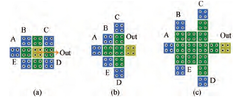
In the literature, many designs for 5-input majority gates have been suggested. All of these designs are single layer designs. Layouts of three of such designs are shown in Figure 8.

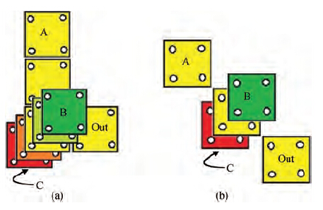
In Reference [18], the layout shown in Figure 8(a) was proposed. It uses ten cells and the output can be taken out from the middle cell through multilayer wire crossing. The layout in Figure 8(b) is proposed in Reference [20]. This design also employs ten QCA cells. But due to the proximity of its input cells, it is very difficult to connect all of the inputs to the majority gate while ensuring that there is no cross talk between the inputs. Hence this design is not so reliable. The majority gate in Figure 8(c) is proposed in Reference [21]. In this layout the inputs have been separated from each other, so that the majority gate can now be connected to the inputs without having any cross talk between the inputs. But in order to make it more reliable, the number of QCA cells has been increased significantly. This design uses 18 QCA cells. In this paper, a 5-input majority gate design has been proposed, which uses the fundamental concepts of the multilayer gate design paradigm. The design of the proposed majority gate is spread over five layers. It is designed by placing three input cells in the plane of the driver cell and the other two input cells are out of the plane of the driver cell. An illustration of this is shown in Figure 9.
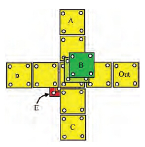
In this design, three of the five inputs, A, C and D, are placed in the same layer as the driver cell. Thus they will try to induce the same polarity in the drive cell as they have themself. Inputs B and E are two layers away from the driver cell in opposite directions. Their signal will reach the driver cell after two inversions and hence be the same as the original signal. So, inputs B and E will also try to force their polarity on the driver cell. We can see the symmetry of all five inputs with respect to the driver cells and they are all trying to induce the same polarity as their own in the driver cell. Hence we obtain a majority voter. The state which is in the majority in the inputs will be reflected in the output.
5. Adder design in the multilayer gate design paradigm
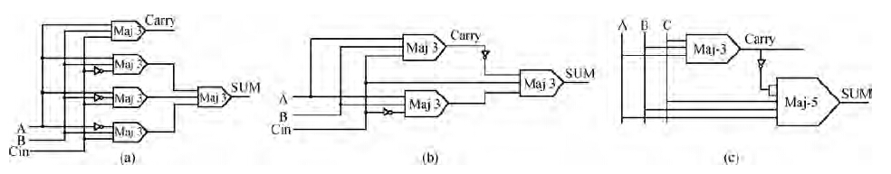
Since 1994, when the first adder design was proposed in QCA technology, many researchers have worked in the field of adder design. With the passage of time more and more efficient algorithms have been proposed in the literature for adder design. Schematics of three of such designs are shown in Figure 10. The schematic in Figure 10(a) uses five 3-input majority gates and three inverters[11], that in Figure 10(b) uses three 3-input majority gates and two inverters[22] and that in Figure~10(c) uses one 3-input majority gate, one 5-input majority gate and one inverter[18].

In this paper 1-bit and 2-bit adders have been designed using an algorithm proposed in Reference [18] (Figure 10(c)) in the multilayer gate design paradigm. To appreciate the advantages that are achieved by designing a circuit in a multilayer, their single layer counterparts have also been designed for comparison.
5.1 The 1-bit adder
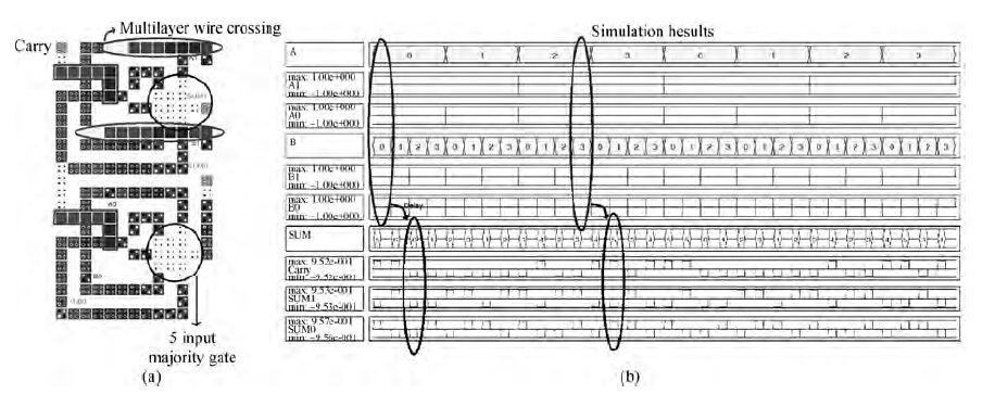
A 1-bit full adder using a 5-input majority gate has been designed in the traditional single layer with multilayer wire crossing and the proposed multilayer gate design paradigm. The layout of the 5-input majority gate shown in Figure 8(c) has been used to design the adder in a single layer (with multilayer wire crossing) (see Figure 11(a)). The 5-input majority gate in Figure 9 has been employed in the design of the adder in the multilayer gate design paradigm (see Figures 12(a)-12(f)). Their simulation results are shown in Figures 11(b) and 12(g), respectively. The site of the 5-input majority gate has been marked in both of the layouts.
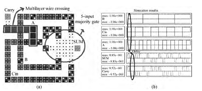
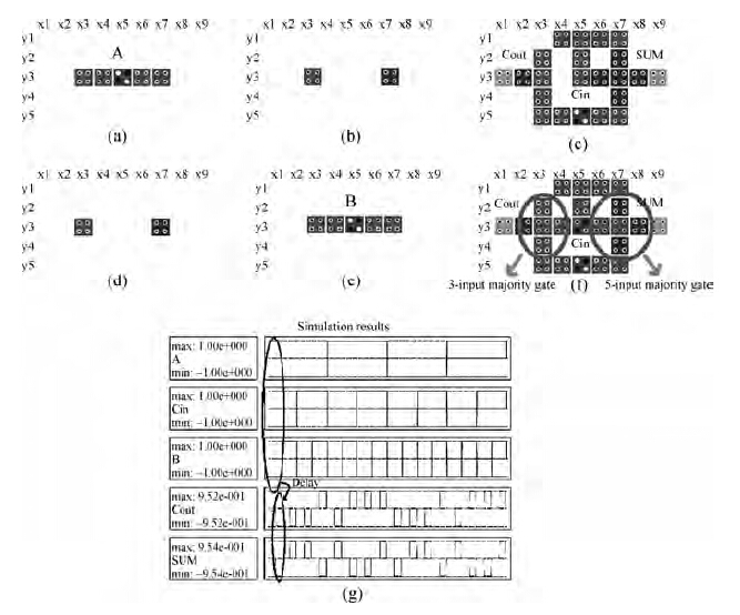
As it is not possible to show a three-dimensional circuit on two-dimensional paper, the layer-wise cell placement has been shown. A coordinate system has also been used to uniquely identify all of the cells. In Figure 12, one can see that input A is given at (x5, y3, z0), where z0 indicates layer-0. From Figure~12, one can also see that the driver cell for the 3-input majority gate is at (x3, y3, z2) and the driver cell for the 5-input majority gate is at (x7, y3, z2). A layer-wise analysis of the two designs is provided in Table 1.
 DownLoad:
CSV
| Show Table
DownLoad:
CSV
| Show Table
5.2 The 2-bit adder
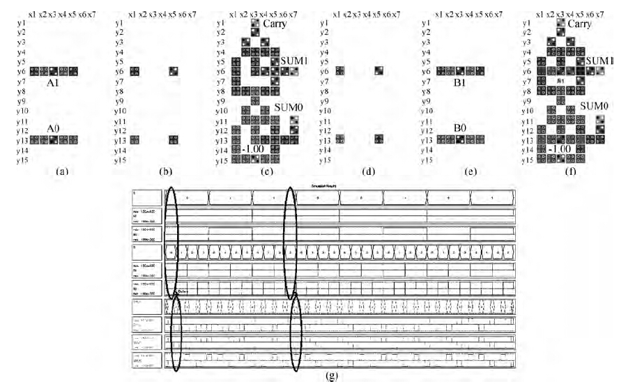
By cascading two 1-bit adders, a 2-bit adder has been designed. The design methods in both of the design paradigms are same as for their respective 1-bit adders. Figures 13(a) and 14(a)-14(f) show the layout of the 2-bit adders in a single layer with multilayer wire crossing and the multilayer gate design paradigm, respectively. In Figures 13(b) and 14(g), the simulation results are presented, respectively.

One can see from Figures 13 and 14 that the 2-bit adder is nothing other than two 1-bit adders placed one after another. In a similar fashion one can go for even higher bit adders. From Figures 13(b) and 14(g), it is evident that delay has decreased to a great extent; a proper comparison will be performed in the following section. Layer-wise analyses of the two designs are provided in Table 2.
 DownLoad:
CSV
| Show Table
DownLoad:
CSV
| Show Table
6. A comparison between the circuits in the single and multilayer design paradigms
Four parameters have been considered in comparing a circuit drawn in the two design paradigms. They are the number of QCA cells required, the input-output delay, the total area and maximum area. In the traditional single layer design, most of the cells are placed in a single layer, except for the few cells which are part of the multilayer wire crossing. As cells in layers other than the main layer are very few, they are ignored in the area calculation. But in the multilayer gate design paradigm, cells in layers other than the main layer (layer-0) are not negligible. This can be verified from Tables 1 and 2. Therefore the area of the rest of the layers cannot be ignored in the multilayer design. By intuition, one will try to consider total area as one of the comparison parameters, but maximum area is also equally important, as it is the actual floor area that the circuit will occupy.
6.1 A comparison of the 1-bit full adder
From Table 3, one can see that the number of QCA cells required has decreased to less than half in the proposed design paradigm. The proposed design uses only 45 % of the QCA cells of the single layer design. The delay has also been reduced to one-third of the initial design. Total as well as maximum areas in the second design are also 50 % or less than those of the first design. This comparison shows that designing a circuit in the multilayer gate design paradigm can improve the circuit drastically in terms of area, performance and QCA cell requirement.
DownLoad:
CSV
| Show Table
6.2 A comparison of the 2-bit adder
In the case of the 2-bit adder, from Table 4 one can see that the QCA cells requirement has dropped by 61 %. The delay has improved by 71 %. Both the total area and maximum area are one-third in the later design, with respect to the initial design. In the 2-bit adder case we can also see that all the parameters of the circuit designed in the multilayer wire crossing have improved by around 60 %-70 %, which is even better than the 1-bit adder result. As the circuit becomes bigger, more dead-zones (where no cells are placed, so as to avoid cross talk between the wires) are generated in the circuits. By distributing the cells in different layers, dead-zones are avoided and the circuit becomes compact. Hence the larger the circuit becomes, the more efficient will be its multilayer design.
DownLoad:
CSV
| Show Table
6.3 A comparison with circuits reported previously in the literature
From Table 5, it is evident that the QCA cell requirement and the delay in output have significantly improved in the circuit proposed in this paper, designed in the multilayer gate design paradigm. The QCA cell requirement has dropped by 40 % and the delay has reduced to one-third of the best available circuit in Reference [18].
DownLoad:
CSV
| Show Table
7. Design methodology and simulation tools
Before designing any circuit in a simulator, the underlying logic is deduced and then simplified to the level of majority gates and inverters which are the fundamental building blocks in QCA technology. QCADesigner has been used to simulate the designed circuits in this paper. This software is the product of ongoing research of the Konrad Walus group at Calgary University and Notre Dame University. This software is an open source software written in C/C++, which facilitates researchers in integrating their own requirements. As per the software, the cell size is 18 nm with a distance between adjacent cells of 2 nm which is obviously very difficult to achieve with modern lithography[24]. For all the circuits designed in this paper, the following setup has been used for simulations in QCADesigner. The cell dimensions are 18 × 18 nm2. The center to center distance of the cells is 20 nm. The gap between two cells is 2 nm. The separation between two layers is 11.5 nm. The simulation engine used is the Coherence vector engine.
8. Major concerns and scope for future work
A major concern of the proposed multilayer gate design paradigm is the complexity of fabrication due to the involvement of a multiple layer structure. While a number of single layer structures have been demonstrated, no prototypes of QCA designs have been manufactured to date which employ multilayer structures such as multilayer wire crossing.
The proposed multilayer gate design paradigm, however, is inspired by and is by far an extension of multilayer wire crossing. Coplanar wire crossing uses two types of cells: regular and 45∘ rotated cells. Rotated cells reduce the cross talk between the wires at the crossover junction. However, they also add complexity in the fabrication of the crossover junction. Such coplanar wire crossing is also very sensitive to cell misalignment[13] and has very low tolerance of noise[25, 26]. Multilayer wire crossing has shown better reliability results in simulations[27]. Hence many QCA designs in the literature utilize multilayer wire crossing. With ongoing experiments in the physical implementation of QCA circuits, it is expected that fabrication technology will advance to enable the fabrication of multilayer structures in QCA technology. A quantitative comparison in terms of fabrication complexity and fabrication cost can only be performed when fabrication technology in QCA matures with time, enabling large scale fabrication of QCA devices. To date QCA devices have only been fabricated in the laboratory environment at very low temperatures. An optimization will be needed between the increased fabrication cost and advantages for circuits in terms of area, latency and number of QCA cell required, by employing multilayer gates in the circuit design.
The multilayer gate design significantly increases the design complexity, as current simulation tools do not allow three-dimensional visualization of the circuit. But the increased design complexity also gives the designer the freedom to customize, as the addition of a third spatial dimension provides many alternative arrangements of QCA cells for designing QCA circuits.
In this paper, the issue of reliability has not been addressed. Further research can be carried out to determine the fault tolerance of the proposed design paradigm.
9. Conclusion
In the proposed design paradigm, circuits are significantly faster than their single layer counterparts. Both the total area as well as maximum area decrease to less than half in the multilayer design paradigm. Circuits in the multilayer are also economical in terms of material requirements; as the number of QCA cells required also drops by 50 % in the multilayer design, but the cost of fabrication will be higher. All these benefits in the multilayer design are due to the fact that circuits become compact in the multilayer. As there is now no restriction on cells being placed in one layer only, two logic blocks can be brought closer together by designing them in two different layers, one above the other. Hence the wastage of area and QCA cells decreases in the form of wires. As the circuit becomes compact and the number of QCA cells decreases; so the requirement for clocking zones is also reduced. Hence the lower delay in the multilayer design. Above all, multilayer design gives circuit designers the freedom to customize their designs according to the needs of a particular circuit block, as there is no fixed design for the fundamental building blocks in the multilayer gate design paradigm.

 DownLoad: