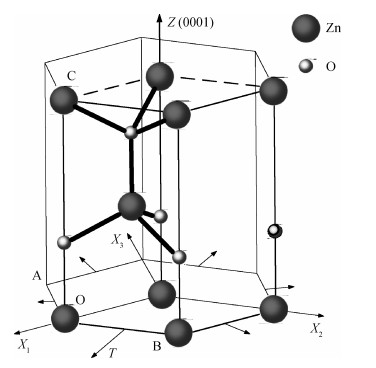
Fig. 1.
Cell of a (0001) wurtzite ZnO crystal.
SEMICONDUCTOR MATERIALS
Liping Qiao1, 2, , Changchun Chai1, Yintang Yang1, Xinhai Yu1 and Chunlei Shi1
Corresponding author: Qiao Liping, Email:lpqiao@126.com
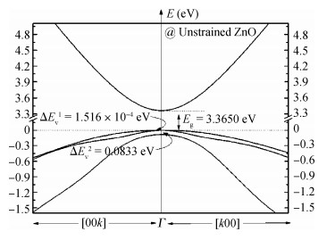
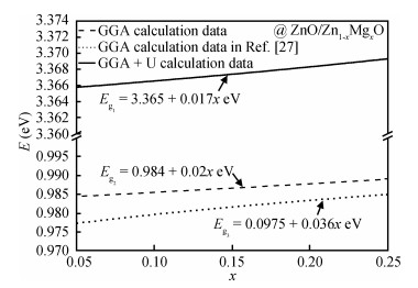
Abstract: Band structures in wurtzite bulk ZnO/Zn1-xMgxO are calculated using first-principles based on the framework of generalized gradient approximation to density functional theory with the introduction of the on-site Coulomb interaction. Strain effects on band gap, splitting energies of valence bands, electron and hole effective masses in strained bulk ZnO are discussed. According to the results, the band gap increases gradually with increasing stress in strained ZnO as an Mg content of Zn1-xMgxO substrate less than 0.3, which is consistent with the experimental results. It is further demonstrated that electron mass of conduction band (CB) under stress increases slightly. There are almost no changes in effective masses of light hole band (LHB) and heavy hole band (HHB) along[00k] and[k00] directions under stress, and stress leads to an obvious decrease in effective masses of crystal splitting band (CSB) along the same directions.
Keywords: GGA + U, band gap, splitting energies, electron mass
| [1] |
Stölzel M, Kupper J, Brandt M, et al. Electronic and optical properties of ZnO/(Mg, Zn)O quantum wells with and without a distinct quantum-confined Stark effect. J Appl Phys, 2012, 111(6): 063701 doi: 10.1063/1.3693555
|
| [2] |
Xu L Z, Liu Y L, Zhou H B, et al. Ideal strengths, structure transitions, and bonding properties of a ZnO single crystal under tension. J Phys: Condensed Matter, 2009, 21(49): 495402 doi: 10.1088/0953-8984/21/49/495402
|
| [3] |
Xiong W, Li S S. The electronic structure of strained ZnO/MgxZn1-xO superlattices and the influence of polarization. Physica E, 2009, 41(3): 506 doi: 10.1016/j.physe.2008.09.013
|
| [4] |
Chauveau J M, Teisseire M, Chauveau H K, et al. Anisotropic strain effects on the photoluminescence emission from heteroepitaxial and homoepitaxial nonpolar (Zn, Mg)O/ZnO quantum wells. J Appl Phys, 2011, 109(10): 102420 doi: 10.1063/1.3578636
|
| [5] |
Aoumeur-Benkabou F Z, Ameri M, Kadoun A, et al. Theoretical study on the origins of the gap bowing in MgxZn1-xO alloys. Modeling and Numerical Simulation of Material Science, 2012, 2: 60 doi: 10.4236/mnsms.2012.23007
|
| [6] |
Nakano M, Tsukazaki A, Ueno K, et al. Spatial distribution of two-dimensional electron gas in a ZnO/Mg0.2Zn0.8O heterostructure probed with a conducting polymer Schottky contact. Appl Phys Lett, 2010, 96(5): 052116 doi: 10.1063/1.3309699
|
| [7] |
Fan W J, Abiyasa A P, Tan S T, et al. Electronic structures of wurtzite ZnO and ZnO/MgxZn1-xO quantum wells. J Cryst Growth, 2006, 287(1): 28 doi: 10.1016/j.jcrysgro.2005.10.037
|
| [8] |
Zitouni K, Kadri A. Effects of lattice-mismatch induced built-in strain on the valence band properties of wurtzite ZnO/MgxZn1-xO quantum well heterostructures. Phys Status Solidi, 2007, 4(1): 208 doi: 10.1002/(ISSN)1610-1642
|
| [9] |
Fan W J, Xia J B, Agus P A, et al. Band parameters and electronic structure of wurtzite ZnO and Zno/MgZnO quantum wells. J Appl Phys, 2006, 99(1): 013702 doi: 10.1063/1.2150266
|
| [10] |
Saniz R, Xu Y, Matsubara, et al. A simplified approach to the band gap correction of defect formation energies: Al, Ga, and In-doped ZnO. J Phys Chem Solids, 2013, 74(1): 45 doi: 10.1016/j.jpcs.2012.07.017
|
| [11] |
Andrei M, David V. First-principles study of polarization in Zn1-xMgxO. Phys Rev B, 2007, 75: 045106 doi: 10.1103/PhysRevB.75.045106
|
| [12] |
Lin H X, Jing S, Yu L C, et al. Optical and structural properties of ZnO/ZnMgO composite thin films prepared by sol-gel technique. J Alloys Compounds, 2013, 548: 155 doi: 10.1016/j.jallcom.2012.09.043
|
| [13] |
Sua S C, Ling C C, Lu Y M, et al. The optical properties of high quality ZnO/ZnMgO quantum wells on Si(111) substrates. Solid State Commun, 2012, 152(4): 311 doi: 10.1016/j.ssc.2011.11.022
|
| [14] |
Su S C, Lv Y M. Ultraviolet electroluminescence of ZnMgO/n-ZnO/ZnMgO/p-GaN heterojunction light emitting diode. Chinese Journal of Luminescence, 2011, 32(8): 821 doi: 10.3788/fgxb
|
| [15] |
Hao L, Guo J F, Song Z L, et al. A ZnO/ZnMgO multiple-quantum-well ultraviolet random laser diode. IEEE Electron Device Lett, 2011, 32(1): 54 doi: 10.1109/LED.2010.2089424
|
| [16] |
Hung C C, ANAS M, John Z, et al. Room-temperature quantum cascade laser: ZnO/Zn1-xMgxO versus GaN/AlxGa1-xN. J Electron Mater, 2013, 42(5): 882 doi: 10.1007/s11664-013-2548-5
|
| [17] |
Huang G Y, Wang C Y, Wang J T. Detailed check of the LDA + U and GGA + U corrected method for defect calculations in wurtzite ZnO. Computer Phys Commun, 2012, 183(8): 1749 doi: 10.1016/j.cpc.2012.03.017
|
| [18] |
Karazhanova S Z, Ravindrana B P, Kjekhusa A. Electronic structure and band parameters for ZnX (X = O, S, Se, Te). J Cryst Growth, 2006, 287: 162 doi: 10.1016/j.jcrysgro.2005.10.061
|
| [19] |
Fan X F, Sun H D, Shen Z X, et al. A first-principle analysis an the phase stabilities, chemical bonds and band gaps of wurtzite structure AxZn1-x alloys (A = Ca, Cd, Mg). J Phys: Condensed Matter, 2008, 20(23): 235221 doi: 10.1088/0953-8984/20/23/235221
|
| [20] |
Lai L N, Lian J S, Jiang Q. Optical and electronic properties of wurtzite structure MgxZn1-xO alloys. Chin Phys Lett, 2011, 28(11): 117101 doi: 10.1088/0256-307X/28/11/117101
|
| [21] |
Zitouni K, Kadri A. Effects of lattice-mismatch induced built-in strain on the valence band properties of wurtzite ZnO/MgxZn1-xO quantum well heterostructures. Phys Status Solidi, 2007, 4(1): 208 doi: 10.1002/(ISSN)1610-1642
|
| [22] |
Zhou G C, Sun X Z, Zhong X L, et al. First-principle study on bonding mechanism of ZnO by LDA + U method. Phys Lett A, 2007, 368(1): 112 http://www.sciencedirect.com/science/article/pii/S0375960107004781
|
| [23] |
Janotti A, Van de Walle C G. LDA + U and hybrid functional calculations for defects in ZnO, SnO2, and TiO2. Phys Status Solidi B, 2011, 248(4): 799 doi: 10.1002/pssb.v248.4
|
| [24] |
Sheetz R M, Richter E, Antonis N, et al. Defect-induced optical absorption in the visible range in ZnO nanowires. Phys Rev B, 2009, 80(19): 195314 doi: 10.1103/PhysRevB.80.195314
|
| [25] |
Wang Q. B, Zhou C, Wu J, et al. A GGA + U study of the optical properties of vanadium doped ZnO with and without single intrinsic vacancy. Opt Commun, 2013, 297: 79 doi: 10.1016/j.optcom.2013.01.073
|
| [26] |
Wang L, Maxisch T, Ceder G. A first-principles approach to studying the thermal stability of oxide cathode materials. Phys Rev B: Condensed Matter, 2006, 73: 195107 doi: 10.1103/PhysRevB.73.195107
|
| [27] |
Gai Y Q, Yao B, Lu Y M, et al. Electronic and optical properties of ZnO thin film under in-plane biaxial strains: ab initio calculation. Phys Lett A, 2007, 372: 72 doi: 10.1016/j.physleta.2007.07.001
|
| [28] |
Li Y F, Yao B, Lu Y M, et al. Biaxial stress-dependent optical band gap, crystalline, and electronic structure in wurtzite ZnO: experimental and ab initio study. J Appl Phys, 2008, 104(8): 083516 doi: 10.1063/1.3000601
|
| [29] |
Alahmed Z, Fu H X. Polar semiconductor ZnO under inplane tensile strain. Phys Rev B, 2008, 77(4): 045213 doi: 10.1103/PhysRevB.77.045213
|
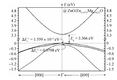
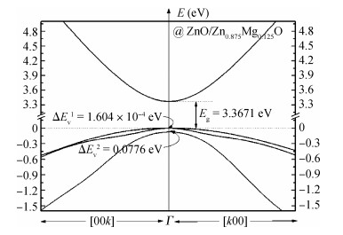
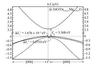
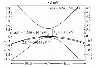
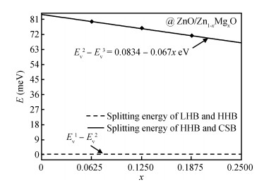
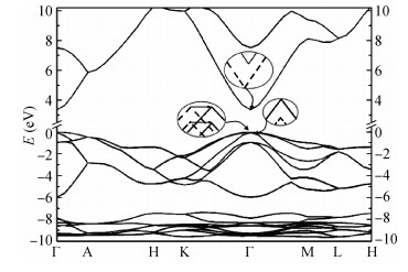
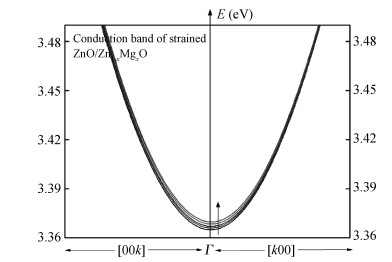
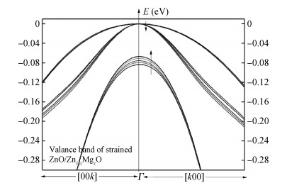
Table 1. Values used in the calculation.

|
Table 2. Values of strained ZnO lattice parameters.

|
| [1] |
Stölzel M, Kupper J, Brandt M, et al. Electronic and optical properties of ZnO/(Mg, Zn)O quantum wells with and without a distinct quantum-confined Stark effect. J Appl Phys, 2012, 111(6): 063701 doi: 10.1063/1.3693555
|
| [2] |
Xu L Z, Liu Y L, Zhou H B, et al. Ideal strengths, structure transitions, and bonding properties of a ZnO single crystal under tension. J Phys: Condensed Matter, 2009, 21(49): 495402 doi: 10.1088/0953-8984/21/49/495402
|
| [3] |
Xiong W, Li S S. The electronic structure of strained ZnO/MgxZn1-xO superlattices and the influence of polarization. Physica E, 2009, 41(3): 506 doi: 10.1016/j.physe.2008.09.013
|
| [4] |
Chauveau J M, Teisseire M, Chauveau H K, et al. Anisotropic strain effects on the photoluminescence emission from heteroepitaxial and homoepitaxial nonpolar (Zn, Mg)O/ZnO quantum wells. J Appl Phys, 2011, 109(10): 102420 doi: 10.1063/1.3578636
|
| [5] |
Aoumeur-Benkabou F Z, Ameri M, Kadoun A, et al. Theoretical study on the origins of the gap bowing in MgxZn1-xO alloys. Modeling and Numerical Simulation of Material Science, 2012, 2: 60 doi: 10.4236/mnsms.2012.23007
|
| [6] |
Nakano M, Tsukazaki A, Ueno K, et al. Spatial distribution of two-dimensional electron gas in a ZnO/Mg0.2Zn0.8O heterostructure probed with a conducting polymer Schottky contact. Appl Phys Lett, 2010, 96(5): 052116 doi: 10.1063/1.3309699
|
| [7] |
Fan W J, Abiyasa A P, Tan S T, et al. Electronic structures of wurtzite ZnO and ZnO/MgxZn1-xO quantum wells. J Cryst Growth, 2006, 287(1): 28 doi: 10.1016/j.jcrysgro.2005.10.037
|
| [8] |
Zitouni K, Kadri A. Effects of lattice-mismatch induced built-in strain on the valence band properties of wurtzite ZnO/MgxZn1-xO quantum well heterostructures. Phys Status Solidi, 2007, 4(1): 208 doi: 10.1002/(ISSN)1610-1642
|
| [9] |
Fan W J, Xia J B, Agus P A, et al. Band parameters and electronic structure of wurtzite ZnO and Zno/MgZnO quantum wells. J Appl Phys, 2006, 99(1): 013702 doi: 10.1063/1.2150266
|
| [10] |
Saniz R, Xu Y, Matsubara, et al. A simplified approach to the band gap correction of defect formation energies: Al, Ga, and In-doped ZnO. J Phys Chem Solids, 2013, 74(1): 45 doi: 10.1016/j.jpcs.2012.07.017
|
| [11] |
Andrei M, David V. First-principles study of polarization in Zn1-xMgxO. Phys Rev B, 2007, 75: 045106 doi: 10.1103/PhysRevB.75.045106
|
| [12] |
Lin H X, Jing S, Yu L C, et al. Optical and structural properties of ZnO/ZnMgO composite thin films prepared by sol-gel technique. J Alloys Compounds, 2013, 548: 155 doi: 10.1016/j.jallcom.2012.09.043
|
| [13] |
Sua S C, Ling C C, Lu Y M, et al. The optical properties of high quality ZnO/ZnMgO quantum wells on Si(111) substrates. Solid State Commun, 2012, 152(4): 311 doi: 10.1016/j.ssc.2011.11.022
|
| [14] |
Su S C, Lv Y M. Ultraviolet electroluminescence of ZnMgO/n-ZnO/ZnMgO/p-GaN heterojunction light emitting diode. Chinese Journal of Luminescence, 2011, 32(8): 821 doi: 10.3788/fgxb
|
| [15] |
Hao L, Guo J F, Song Z L, et al. A ZnO/ZnMgO multiple-quantum-well ultraviolet random laser diode. IEEE Electron Device Lett, 2011, 32(1): 54 doi: 10.1109/LED.2010.2089424
|
| [16] |
Hung C C, ANAS M, John Z, et al. Room-temperature quantum cascade laser: ZnO/Zn1-xMgxO versus GaN/AlxGa1-xN. J Electron Mater, 2013, 42(5): 882 doi: 10.1007/s11664-013-2548-5
|
| [17] |
Huang G Y, Wang C Y, Wang J T. Detailed check of the LDA + U and GGA + U corrected method for defect calculations in wurtzite ZnO. Computer Phys Commun, 2012, 183(8): 1749 doi: 10.1016/j.cpc.2012.03.017
|
| [18] |
Karazhanova S Z, Ravindrana B P, Kjekhusa A. Electronic structure and band parameters for ZnX (X = O, S, Se, Te). J Cryst Growth, 2006, 287: 162 doi: 10.1016/j.jcrysgro.2005.10.061
|
| [19] |
Fan X F, Sun H D, Shen Z X, et al. A first-principle analysis an the phase stabilities, chemical bonds and band gaps of wurtzite structure AxZn1-x alloys (A = Ca, Cd, Mg). J Phys: Condensed Matter, 2008, 20(23): 235221 doi: 10.1088/0953-8984/20/23/235221
|
| [20] |
Lai L N, Lian J S, Jiang Q. Optical and electronic properties of wurtzite structure MgxZn1-xO alloys. Chin Phys Lett, 2011, 28(11): 117101 doi: 10.1088/0256-307X/28/11/117101
|
| [21] |
Zitouni K, Kadri A. Effects of lattice-mismatch induced built-in strain on the valence band properties of wurtzite ZnO/MgxZn1-xO quantum well heterostructures. Phys Status Solidi, 2007, 4(1): 208 doi: 10.1002/(ISSN)1610-1642
|
| [22] |
Zhou G C, Sun X Z, Zhong X L, et al. First-principle study on bonding mechanism of ZnO by LDA + U method. Phys Lett A, 2007, 368(1): 112 http://www.sciencedirect.com/science/article/pii/S0375960107004781
|
| [23] |
Janotti A, Van de Walle C G. LDA + U and hybrid functional calculations for defects in ZnO, SnO2, and TiO2. Phys Status Solidi B, 2011, 248(4): 799 doi: 10.1002/pssb.v248.4
|
| [24] |
Sheetz R M, Richter E, Antonis N, et al. Defect-induced optical absorption in the visible range in ZnO nanowires. Phys Rev B, 2009, 80(19): 195314 doi: 10.1103/PhysRevB.80.195314
|
| [25] |
Wang Q. B, Zhou C, Wu J, et al. A GGA + U study of the optical properties of vanadium doped ZnO with and without single intrinsic vacancy. Opt Commun, 2013, 297: 79 doi: 10.1016/j.optcom.2013.01.073
|
| [26] |
Wang L, Maxisch T, Ceder G. A first-principles approach to studying the thermal stability of oxide cathode materials. Phys Rev B: Condensed Matter, 2006, 73: 195107 doi: 10.1103/PhysRevB.73.195107
|
| [27] |
Gai Y Q, Yao B, Lu Y M, et al. Electronic and optical properties of ZnO thin film under in-plane biaxial strains: ab initio calculation. Phys Lett A, 2007, 372: 72 doi: 10.1016/j.physleta.2007.07.001
|
| [28] |
Li Y F, Yao B, Lu Y M, et al. Biaxial stress-dependent optical band gap, crystalline, and electronic structure in wurtzite ZnO: experimental and ab initio study. J Appl Phys, 2008, 104(8): 083516 doi: 10.1063/1.3000601
|
| [29] |
Alahmed Z, Fu H X. Polar semiconductor ZnO under inplane tensile strain. Phys Rev B, 2008, 77(4): 045213 doi: 10.1103/PhysRevB.77.045213
|


Article views: 4684 Times PDF downloads: 85 Times Cited by: 0 Times
Received: 13 December 2013 Revised: 02 February 2014 Online: Published: 01 July 2014
| Citation: |
Liping Qiao, Changchun Chai, Yintang Yang, Xinhai Yu, Chunlei Shi. Strain effects on band structure of wurtzite ZnO: a GGA + U study[J]. Journal of Semiconductors, 2014, 35(7): 073004. doi: 10.1088/1674-4926/35/7/073004
****
L P Qiao, C C Chai, Y T Yang, X H Yu, C L Shi. Strain effects on band structure of wurtzite ZnO: a GGA + U study[J]. J. Semicond., 2014, 35(7): 073004. doi: 10.1088/1674-4926/35/7/073004.

|
| [1] |
Stölzel M, Kupper J, Brandt M, et al. Electronic and optical properties of ZnO/(Mg, Zn)O quantum wells with and without a distinct quantum-confined Stark effect. J Appl Phys, 2012, 111(6): 063701 doi: 10.1063/1.3693555
|
| [2] |
Xu L Z, Liu Y L, Zhou H B, et al. Ideal strengths, structure transitions, and bonding properties of a ZnO single crystal under tension. J Phys: Condensed Matter, 2009, 21(49): 495402 doi: 10.1088/0953-8984/21/49/495402
|
| [3] |
Xiong W, Li S S. The electronic structure of strained ZnO/MgxZn1-xO superlattices and the influence of polarization. Physica E, 2009, 41(3): 506 doi: 10.1016/j.physe.2008.09.013
|
| [4] |
Chauveau J M, Teisseire M, Chauveau H K, et al. Anisotropic strain effects on the photoluminescence emission from heteroepitaxial and homoepitaxial nonpolar (Zn, Mg)O/ZnO quantum wells. J Appl Phys, 2011, 109(10): 102420 doi: 10.1063/1.3578636
|
| [5] |
Aoumeur-Benkabou F Z, Ameri M, Kadoun A, et al. Theoretical study on the origins of the gap bowing in MgxZn1-xO alloys. Modeling and Numerical Simulation of Material Science, 2012, 2: 60 doi: 10.4236/mnsms.2012.23007
|
| [6] |
Nakano M, Tsukazaki A, Ueno K, et al. Spatial distribution of two-dimensional electron gas in a ZnO/Mg0.2Zn0.8O heterostructure probed with a conducting polymer Schottky contact. Appl Phys Lett, 2010, 96(5): 052116 doi: 10.1063/1.3309699
|
| [7] |
Fan W J, Abiyasa A P, Tan S T, et al. Electronic structures of wurtzite ZnO and ZnO/MgxZn1-xO quantum wells. J Cryst Growth, 2006, 287(1): 28 doi: 10.1016/j.jcrysgro.2005.10.037
|
| [8] |
Zitouni K, Kadri A. Effects of lattice-mismatch induced built-in strain on the valence band properties of wurtzite ZnO/MgxZn1-xO quantum well heterostructures. Phys Status Solidi, 2007, 4(1): 208 doi: 10.1002/(ISSN)1610-1642
|
| [9] |
Fan W J, Xia J B, Agus P A, et al. Band parameters and electronic structure of wurtzite ZnO and Zno/MgZnO quantum wells. J Appl Phys, 2006, 99(1): 013702 doi: 10.1063/1.2150266
|
| [10] |
Saniz R, Xu Y, Matsubara, et al. A simplified approach to the band gap correction of defect formation energies: Al, Ga, and In-doped ZnO. J Phys Chem Solids, 2013, 74(1): 45 doi: 10.1016/j.jpcs.2012.07.017
|
| [11] |
Andrei M, David V. First-principles study of polarization in Zn1-xMgxO. Phys Rev B, 2007, 75: 045106 doi: 10.1103/PhysRevB.75.045106
|
| [12] |
Lin H X, Jing S, Yu L C, et al. Optical and structural properties of ZnO/ZnMgO composite thin films prepared by sol-gel technique. J Alloys Compounds, 2013, 548: 155 doi: 10.1016/j.jallcom.2012.09.043
|
| [13] |
Sua S C, Ling C C, Lu Y M, et al. The optical properties of high quality ZnO/ZnMgO quantum wells on Si(111) substrates. Solid State Commun, 2012, 152(4): 311 doi: 10.1016/j.ssc.2011.11.022
|
| [14] |
Su S C, Lv Y M. Ultraviolet electroluminescence of ZnMgO/n-ZnO/ZnMgO/p-GaN heterojunction light emitting diode. Chinese Journal of Luminescence, 2011, 32(8): 821 doi: 10.3788/fgxb
|
| [15] |
Hao L, Guo J F, Song Z L, et al. A ZnO/ZnMgO multiple-quantum-well ultraviolet random laser diode. IEEE Electron Device Lett, 2011, 32(1): 54 doi: 10.1109/LED.2010.2089424
|
| [16] |
Hung C C, ANAS M, John Z, et al. Room-temperature quantum cascade laser: ZnO/Zn1-xMgxO versus GaN/AlxGa1-xN. J Electron Mater, 2013, 42(5): 882 doi: 10.1007/s11664-013-2548-5
|
| [17] |
Huang G Y, Wang C Y, Wang J T. Detailed check of the LDA + U and GGA + U corrected method for defect calculations in wurtzite ZnO. Computer Phys Commun, 2012, 183(8): 1749 doi: 10.1016/j.cpc.2012.03.017
|
| [18] |
Karazhanova S Z, Ravindrana B P, Kjekhusa A. Electronic structure and band parameters for ZnX (X = O, S, Se, Te). J Cryst Growth, 2006, 287: 162 doi: 10.1016/j.jcrysgro.2005.10.061
|
| [19] |
Fan X F, Sun H D, Shen Z X, et al. A first-principle analysis an the phase stabilities, chemical bonds and band gaps of wurtzite structure AxZn1-x alloys (A = Ca, Cd, Mg). J Phys: Condensed Matter, 2008, 20(23): 235221 doi: 10.1088/0953-8984/20/23/235221
|
| [20] |
Lai L N, Lian J S, Jiang Q. Optical and electronic properties of wurtzite structure MgxZn1-xO alloys. Chin Phys Lett, 2011, 28(11): 117101 doi: 10.1088/0256-307X/28/11/117101
|
| [21] |
Zitouni K, Kadri A. Effects of lattice-mismatch induced built-in strain on the valence band properties of wurtzite ZnO/MgxZn1-xO quantum well heterostructures. Phys Status Solidi, 2007, 4(1): 208 doi: 10.1002/(ISSN)1610-1642
|
| [22] |
Zhou G C, Sun X Z, Zhong X L, et al. First-principle study on bonding mechanism of ZnO by LDA + U method. Phys Lett A, 2007, 368(1): 112 http://www.sciencedirect.com/science/article/pii/S0375960107004781
|
| [23] |
Janotti A, Van de Walle C G. LDA + U and hybrid functional calculations for defects in ZnO, SnO2, and TiO2. Phys Status Solidi B, 2011, 248(4): 799 doi: 10.1002/pssb.v248.4
|
| [24] |
Sheetz R M, Richter E, Antonis N, et al. Defect-induced optical absorption in the visible range in ZnO nanowires. Phys Rev B, 2009, 80(19): 195314 doi: 10.1103/PhysRevB.80.195314
|
| [25] |
Wang Q. B, Zhou C, Wu J, et al. A GGA + U study of the optical properties of vanadium doped ZnO with and without single intrinsic vacancy. Opt Commun, 2013, 297: 79 doi: 10.1016/j.optcom.2013.01.073
|
| [26] |
Wang L, Maxisch T, Ceder G. A first-principles approach to studying the thermal stability of oxide cathode materials. Phys Rev B: Condensed Matter, 2006, 73: 195107 doi: 10.1103/PhysRevB.73.195107
|
| [27] |
Gai Y Q, Yao B, Lu Y M, et al. Electronic and optical properties of ZnO thin film under in-plane biaxial strains: ab initio calculation. Phys Lett A, 2007, 372: 72 doi: 10.1016/j.physleta.2007.07.001
|
| [28] |
Li Y F, Yao B, Lu Y M, et al. Biaxial stress-dependent optical band gap, crystalline, and electronic structure in wurtzite ZnO: experimental and ab initio study. J Appl Phys, 2008, 104(8): 083516 doi: 10.1063/1.3000601
|
| [29] |
Alahmed Z, Fu H X. Polar semiconductor ZnO under inplane tensile strain. Phys Rev B, 2008, 77(4): 045213 doi: 10.1103/PhysRevB.77.045213
|

 WeChat ID
Journal of Semiconductors © 2017 All Rights Reserved 京ICP备05085259号-2

 DownLoad: