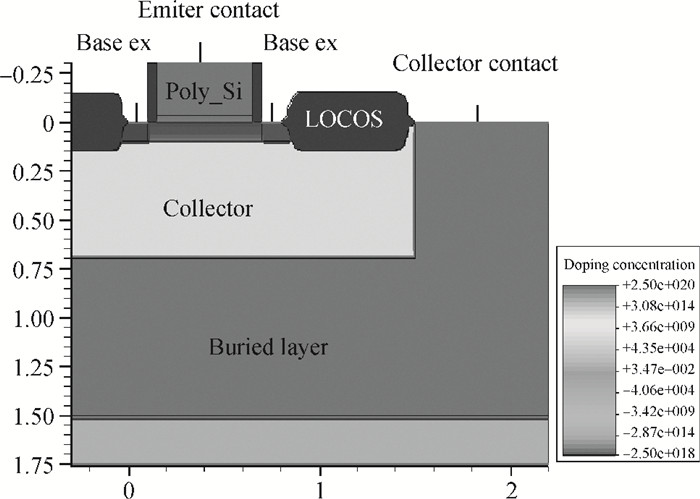
Fig. 1.
Cross-section of a Si/SiGe heterojunction bipolar transistor (HBT).
SEMICONDUCTOR INTEGRATED CIRCUITS
M. Bouhouche1, , S. Latreche1 and C. Gontrand2
Corresponding author: M. Bouhouche, roubilia@yahoo.fr
Abstract: This paper addresses phase noise analysis of a radiofrequency LC oscillator built around a SiGe heterojunction bipolar transistor (HBT) realized in a 0.35 μm BiCMOS process, as an active device. First, we give a brief background to SiGe HBT device physics. The key point is to initiate quantitative analysis on the influence of defects induced during extrinsic base implantation on electric performances of this device. These defects are responsible for the current fluctuations at the origin of low frequency noise in BiCMOS technologies. Next, we investigate the effect of implantation defects as a source of noise in semiconductors on the phase noise of a radiofrequency LC oscillator. We observe their influence on the oscillator phase noise, and we quantify the influence of their energy distribution in the semiconductor gap. Second, we give a behavioral model of an LC oscillator containing a SiGe HBT as an active device. The key goal is to study the susceptibility of a radiofrequency oscillator built around a SiGe HBT to phase noise disturbance sources. Based on the time variance behavior of phase noise in oscillators, transient simulations (in the time domain) were used to analyze the time-dependent noise sensitivity of the oscillator.
Keywords: SiGe heterojunction, radiofrequency, mixed-mode simulations, oscillator, phase noise
| [1] |
Demir A, Mehrota A, Roychowdhury J. Phase noise in oscillators:a unified theory numerical method for characterization. IEEE Circuits and Systems, 2000, 47:655 doi: 10.1109/81.847872
|
| [2] |
Razavi B. A study of phase noise in CMOS oscillators. IEEE J Solid-State Circuits, 1996, 31:331 doi: 10.1109/4.494195
|
| [3] |
Mitin V, Reggiani L, Varani L. Generation-recombination noise in semiconductors. Noise and Fluctuations Control in Electronic Devices, 2003:11 http://adsabs.harvard.edu/abs/1961JPCS...22..391K
|
| [4] |
Cressler J D. SiGe HBT technology:a new contender for Si-based RF and microwave circuit applications. IEEE Trans Microw Theory Tech, 1998, 46:572 doi: 10.1109/22.668665
|
| [5] |
Ramonas M, Sakalas P, Jungemann C, et al. Microscopic modeling of high frequency noise in SiGe HBTS. 37th European Solid State Device Research Conference, 2007:183 http://ieeexplore.ieee.org/document/4430909/
|
| [6] |
Hajimiri A, Lee T H. A general theory of phase noise in electrical oscillator. IEEE J Solid-State Circuits, 1998, 33:179 doi: 10.1109/4.658619
|
| [7] |
Harame D L, Ahlgren D C, Coolbaugh D D, et al. Current status and future trends of SiGe BiCMOS technology. IEEE Trans Electron Devices, 2001, 48:2575 doi: 10.1109/16.960385
|
| [8] |
Baudry H, Szelag B, Deléglise F, et al. BiCMOS7RF:a highly manufacturable 0.25μm BiCMOS RF applications dedicated technology using non-selective SiGeC epitaxy. IEEE Bipolar/BiCMOS Circuits and Technology, 2003:207
|
| [9] |
Mouis M, Gregory H J, Denorme S, et al. Physical modelling of the enhanced diffusion of boron due to ion implantation in thin base NPN bipolar transistors. Microelectron J, 1995, 26:255 doi: 10.1016/0026-2692(95)98927-J
|
| [10] |
Militaru L, Souifi A, Mouis M, et al. Investigation of deep traps in silicon-germanium epitaxial base bipolar transistors with a single polysilicon quasi self aligned architecture. Microelectron Reliab, 2001, 41:253 doi: 10.1016/S0026-2714(00)00097-4
|
| [11] |
ISE: Integrated Systems Engineering (SYNOPSYS), Zurich, Switzerland, DESSIS
|
| [12] |
Pejcinovic B, Tag T W, Navon D H. A comparison of Si and Si1-xGex based BJTs using numerical simulation. IEEE Bipolar Circuits and Technology Meeting, 2006
|
| [13] |
Bouhouche M, Latreche S, Gontrand C. Investigation of process induced defects in SiGe/Si heterojunction bipolar transistors. International Conference of Modelling and Simulation, Algeria, 2007 doi: 10.1116/1.590047
|
| [14] |
Hajimiri A, Lee T. Oscillator phase noise:a tutorials. IEEE J Solid-State Circuits, 2000, 35:326 doi: 10.1109/4.826814
|
| [15] |
Ham D, Hajimiri A. concepts and methods in optimization of integrated LC VCOs. IEEE J Solid-State Circuits, 2001, 36:896 doi: 10.1109/4.924852
|
| [16] |
Hajimiri A, Limotyrakis S, Lee T H. Jitter and phase noise in ring oscillators. IEEE J Solid-State Circuits, 1999, 35:790 http://ieeexplore.ieee.org/document/766813/?arnumber=766813&sortType%3Dasc_p_Sequence%26filter%3DAND(p_IS_Number:16618)
|
| [17] |
Ham D, Hajimiri A. Virtual damping and Einstein relation in oscillators. IEEE J Solid-State Circuits, 2002, 38:407 http://ieeexplore.ieee.org/document/1183847/authors
|


Article views: 3159 Times PDF downloads: 15 Times Cited by: 0 Times
Received: 03 March 2012 Revised: 16 August 2012 Online: Published: 01 February 2013
| Citation: |
M. Bouhouche, S. Latreche, C. Gontrand. Phase noise modeling in LC oscillators implemented in SiGe technology[J]. Journal of Semiconductors, 2013, 34(2): 025001. doi: 10.1088/1674-4926/34/2/025001
****
M. Bouhouche, S. Latreche, C. Gontrand. Phase noise modeling in LC oscillators implemented in SiGe technology[J]. J. Semicond., 2013, 34(2): 025001. doi: 10.1088/1674-4926/34/2/025001.

|
| [1] |
Demir A, Mehrota A, Roychowdhury J. Phase noise in oscillators:a unified theory numerical method for characterization. IEEE Circuits and Systems, 2000, 47:655 doi: 10.1109/81.847872
|
| [2] |
Razavi B. A study of phase noise in CMOS oscillators. IEEE J Solid-State Circuits, 1996, 31:331 doi: 10.1109/4.494195
|
| [3] |
Mitin V, Reggiani L, Varani L. Generation-recombination noise in semiconductors. Noise and Fluctuations Control in Electronic Devices, 2003:11 http://adsabs.harvard.edu/abs/1961JPCS...22..391K
|
| [4] |
Cressler J D. SiGe HBT technology:a new contender for Si-based RF and microwave circuit applications. IEEE Trans Microw Theory Tech, 1998, 46:572 doi: 10.1109/22.668665
|
| [5] |
Ramonas M, Sakalas P, Jungemann C, et al. Microscopic modeling of high frequency noise in SiGe HBTS. 37th European Solid State Device Research Conference, 2007:183 http://ieeexplore.ieee.org/document/4430909/
|
| [6] |
Hajimiri A, Lee T H. A general theory of phase noise in electrical oscillator. IEEE J Solid-State Circuits, 1998, 33:179 doi: 10.1109/4.658619
|
| [7] |
Harame D L, Ahlgren D C, Coolbaugh D D, et al. Current status and future trends of SiGe BiCMOS technology. IEEE Trans Electron Devices, 2001, 48:2575 doi: 10.1109/16.960385
|
| [8] |
Baudry H, Szelag B, Deléglise F, et al. BiCMOS7RF:a highly manufacturable 0.25μm BiCMOS RF applications dedicated technology using non-selective SiGeC epitaxy. IEEE Bipolar/BiCMOS Circuits and Technology, 2003:207
|
| [9] |
Mouis M, Gregory H J, Denorme S, et al. Physical modelling of the enhanced diffusion of boron due to ion implantation in thin base NPN bipolar transistors. Microelectron J, 1995, 26:255 doi: 10.1016/0026-2692(95)98927-J
|
| [10] |
Militaru L, Souifi A, Mouis M, et al. Investigation of deep traps in silicon-germanium epitaxial base bipolar transistors with a single polysilicon quasi self aligned architecture. Microelectron Reliab, 2001, 41:253 doi: 10.1016/S0026-2714(00)00097-4
|
| [11] |
ISE: Integrated Systems Engineering (SYNOPSYS), Zurich, Switzerland, DESSIS
|
| [12] |
Pejcinovic B, Tag T W, Navon D H. A comparison of Si and Si1-xGex based BJTs using numerical simulation. IEEE Bipolar Circuits and Technology Meeting, 2006
|
| [13] |
Bouhouche M, Latreche S, Gontrand C. Investigation of process induced defects in SiGe/Si heterojunction bipolar transistors. International Conference of Modelling and Simulation, Algeria, 2007 doi: 10.1116/1.590047
|
| [14] |
Hajimiri A, Lee T. Oscillator phase noise:a tutorials. IEEE J Solid-State Circuits, 2000, 35:326 doi: 10.1109/4.826814
|
| [15] |
Ham D, Hajimiri A. concepts and methods in optimization of integrated LC VCOs. IEEE J Solid-State Circuits, 2001, 36:896 doi: 10.1109/4.924852
|
| [16] |
Hajimiri A, Limotyrakis S, Lee T H. Jitter and phase noise in ring oscillators. IEEE J Solid-State Circuits, 1999, 35:790 http://ieeexplore.ieee.org/document/766813/?arnumber=766813&sortType%3Dasc_p_Sequence%26filter%3DAND(p_IS_Number:16618)
|
| [17] |
Ham D, Hajimiri A. Virtual damping and Einstein relation in oscillators. IEEE J Solid-State Circuits, 2002, 38:407 http://ieeexplore.ieee.org/document/1183847/authors
|

 WeChat ID
Journal of Semiconductors © 2017 All Rights Reserved 京ICP备05085259号-2

 DownLoad: