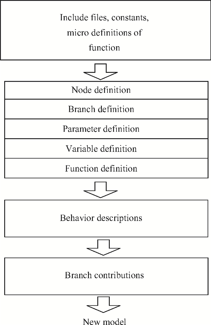
Fig. 1.
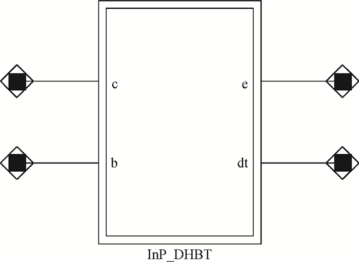
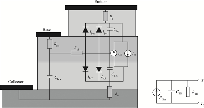
The topology of InP/InGaAs DHBTs with InP emitter, InGaAs base, InP collector.
SEMICONDUCTOR DEVICES
Yuxia Shi1, , Zhi Jin2, Zhijian Pan1, Yongbo Su2, Yuxiong Cao2 and Yan Wang1
Corresponding author: Shi Yuxia, Email:shi_yuxia@163.com
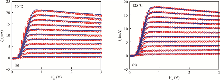
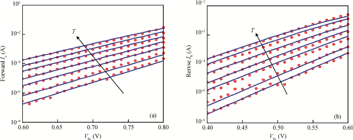
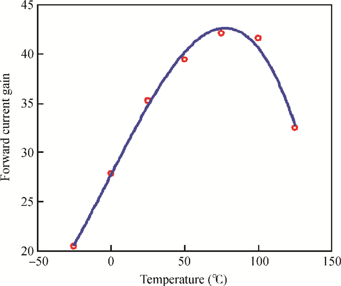
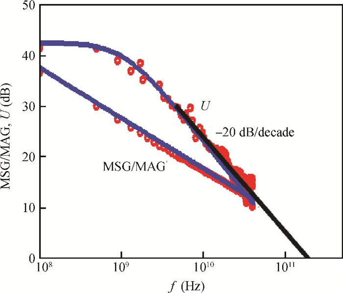
Abstract: A large signal model for InP/InGaAs double heterojunction bipolar transistors including thermal effects has been reported, which demonstrated good agreements of simulations with measurements. On the basis of the previous model in which the double heterojunction effect, current blocking effect and high current effect in current expression are considered, the effect of bandgap narrowing with temperature has been considered in transport current while a formula for model parameters as a function of temperature has been developed. This model is implemented by Verilog-A and embedded in ADS. The proposed model is verified with DC and large signal measurements.
Keywords: large signal model, InP DHBT, temperature effect, bandgap narrowing, Verilog-A
| [1] |
Hacker J, Munkyo S, Young A, et al. THz MMICs based on InP HBT technology. IEEE MTT-S, 2010:1126 http://ieeexplore.ieee.org/document/5518124/authors
|
| [2] |
Snodgrass W, Feng M. Nano-scale type-Ⅱ InP/GaAsSb DHBTs to reach THz cutoff frequencies. CS MANTECH Conference, 2008:277 https://www.researchgate.net/publication/228626456_Nano-scale_type-II_InPGaAsSb_DHBTs_to_reach_THz_cutoff_frequencies
|
| [3] |
Feng M, Shen S C, Caruth D C, et al. Device technologies for RF front-end circuits in next-generation wireless communications. Proc IEEE, 2004, 92(2):354 doi: 10.1109/JPROC.2003.821903
|
| [4] |
Lobisser E, Griffith Z, Jain V, et al. 200-nm InGaAs/InP type Ⅰ DHBT employing a dual-sidewall emitter process demonstrating fmax > 800 GHz and ft=360 GHz. IEEE IPRM, 2009:16
|
| [5] |
Driad R, Makon R E, Benkhelifa F, et al. InP DHBT technology for 100 Gbit/s applications. CS Mantech, 2008
|
| [6] |
Snodgrass W, Wu B R, Cheng K Y, et al. Type-Ⅱ GaAsSb/InP DHBTs with record fT=670 GHz and simultaneous fT, fmax > 400 GHz. IEDM Technical Digest, 2007:623
|
| [7] |
Jin Z, Su Y, Cheng W, et al. Common-base multi-finger submicron InGaAs/InP double heterojunction bipolar transistor with fmax of 305 GHz. Solid-State Electron, 2008:1825
|
| [8] |
Shi Y, Jin Z, Su Y, et al. An improved VBIC model for InP DHBTs. IEEE Radio Frequency Integrated Circuits Symposium (RFIC), 2012:409 http://ieeexplore.ieee.org/document/6242310/?arnumber=6242310&punumber%3D6230821%26sortType%3Dasc_p_Sequence%26filter%3DAND(p_IS_Number:6242137)%26rowsPerPage%3D100
|
| [9] |
Lai J W, Chuang Y J, Feng M, et al. 300 GHz InP DHBT large signal model including current blocking effect and validated by Gilbert multiplier circuits. CSIC, 2005:61 http://ieeexplore.ieee.org/document/1531758/
|
| [10] |
Maloney T J, Prey J. Transient and steady-state electron transport properties of GaAs and InP. J Appl Phys, 1977, 48(2):781 doi: 10.1063/1.323670
|
| [11] |
Dikmen C T, Dogan N S, Osman M A. DC modeling and characterization of AlGaAs/GaAs heterojunction bipolar transistors for high-temperature applications. IEEE J Solid-State Circuits, 1994, 29(2):108 doi: 10.1109/4.272113
|
| [12] |
Jin Z, Su Y, Cheng W, et al. High-breakdown-voltage submicron InGaAs_InP double heterojunction bipolar transistor with ft=170 GHz and fmax=253 GHz. Chin Phys Lett, 2008, 25:2686 doi: 10.1088/0256-307X/25/7/098
|


Article views: 3292 Times PDF downloads: 21 Times Cited by: 0 Times
Received: 20 November 2012 Revised: Online: Published: 01 June 2013
| Citation: |
Yuxia Shi, Zhi Jin, Zhijian Pan, Yongbo Su, Yuxiong Cao, Yan Wang. A Verilog-A large signal model for InP DHBT including thermal effects[J]. Journal of Semiconductors, 2013, 34(6): 064007. doi: 10.1088/1674-4926/34/6/064007
****
Y X Shi, Z Jin, Z J Pan, Y B Su, Y X Cao, Y Wang. A Verilog-A large signal model for InP DHBT including thermal effects[J]. J. Semicond., 2013, 34(6): 064007. doi: 10.1088/1674-4926/34/6/064007.

|
| [1] |
Hacker J, Munkyo S, Young A, et al. THz MMICs based on InP HBT technology. IEEE MTT-S, 2010:1126 http://ieeexplore.ieee.org/document/5518124/authors
|
| [2] |
Snodgrass W, Feng M. Nano-scale type-Ⅱ InP/GaAsSb DHBTs to reach THz cutoff frequencies. CS MANTECH Conference, 2008:277 https://www.researchgate.net/publication/228626456_Nano-scale_type-II_InPGaAsSb_DHBTs_to_reach_THz_cutoff_frequencies
|
| [3] |
Feng M, Shen S C, Caruth D C, et al. Device technologies for RF front-end circuits in next-generation wireless communications. Proc IEEE, 2004, 92(2):354 doi: 10.1109/JPROC.2003.821903
|
| [4] |
Lobisser E, Griffith Z, Jain V, et al. 200-nm InGaAs/InP type Ⅰ DHBT employing a dual-sidewall emitter process demonstrating fmax > 800 GHz and ft=360 GHz. IEEE IPRM, 2009:16
|
| [5] |
Driad R, Makon R E, Benkhelifa F, et al. InP DHBT technology for 100 Gbit/s applications. CS Mantech, 2008
|
| [6] |
Snodgrass W, Wu B R, Cheng K Y, et al. Type-Ⅱ GaAsSb/InP DHBTs with record fT=670 GHz and simultaneous fT, fmax > 400 GHz. IEDM Technical Digest, 2007:623
|
| [7] |
Jin Z, Su Y, Cheng W, et al. Common-base multi-finger submicron InGaAs/InP double heterojunction bipolar transistor with fmax of 305 GHz. Solid-State Electron, 2008:1825
|
| [8] |
Shi Y, Jin Z, Su Y, et al. An improved VBIC model for InP DHBTs. IEEE Radio Frequency Integrated Circuits Symposium (RFIC), 2012:409 http://ieeexplore.ieee.org/document/6242310/?arnumber=6242310&punumber%3D6230821%26sortType%3Dasc_p_Sequence%26filter%3DAND(p_IS_Number:6242137)%26rowsPerPage%3D100
|
| [9] |
Lai J W, Chuang Y J, Feng M, et al. 300 GHz InP DHBT large signal model including current blocking effect and validated by Gilbert multiplier circuits. CSIC, 2005:61 http://ieeexplore.ieee.org/document/1531758/
|
| [10] |
Maloney T J, Prey J. Transient and steady-state electron transport properties of GaAs and InP. J Appl Phys, 1977, 48(2):781 doi: 10.1063/1.323670
|
| [11] |
Dikmen C T, Dogan N S, Osman M A. DC modeling and characterization of AlGaAs/GaAs heterojunction bipolar transistors for high-temperature applications. IEEE J Solid-State Circuits, 1994, 29(2):108 doi: 10.1109/4.272113
|
| [12] |
Jin Z, Su Y, Cheng W, et al. High-breakdown-voltage submicron InGaAs_InP double heterojunction bipolar transistor with ft=170 GHz and fmax=253 GHz. Chin Phys Lett, 2008, 25:2686 doi: 10.1088/0256-307X/25/7/098
|

 WeChat ID
Journal of Semiconductors © 2017 All Rights Reserved 京ICP备05085259号-2

 DownLoad: