


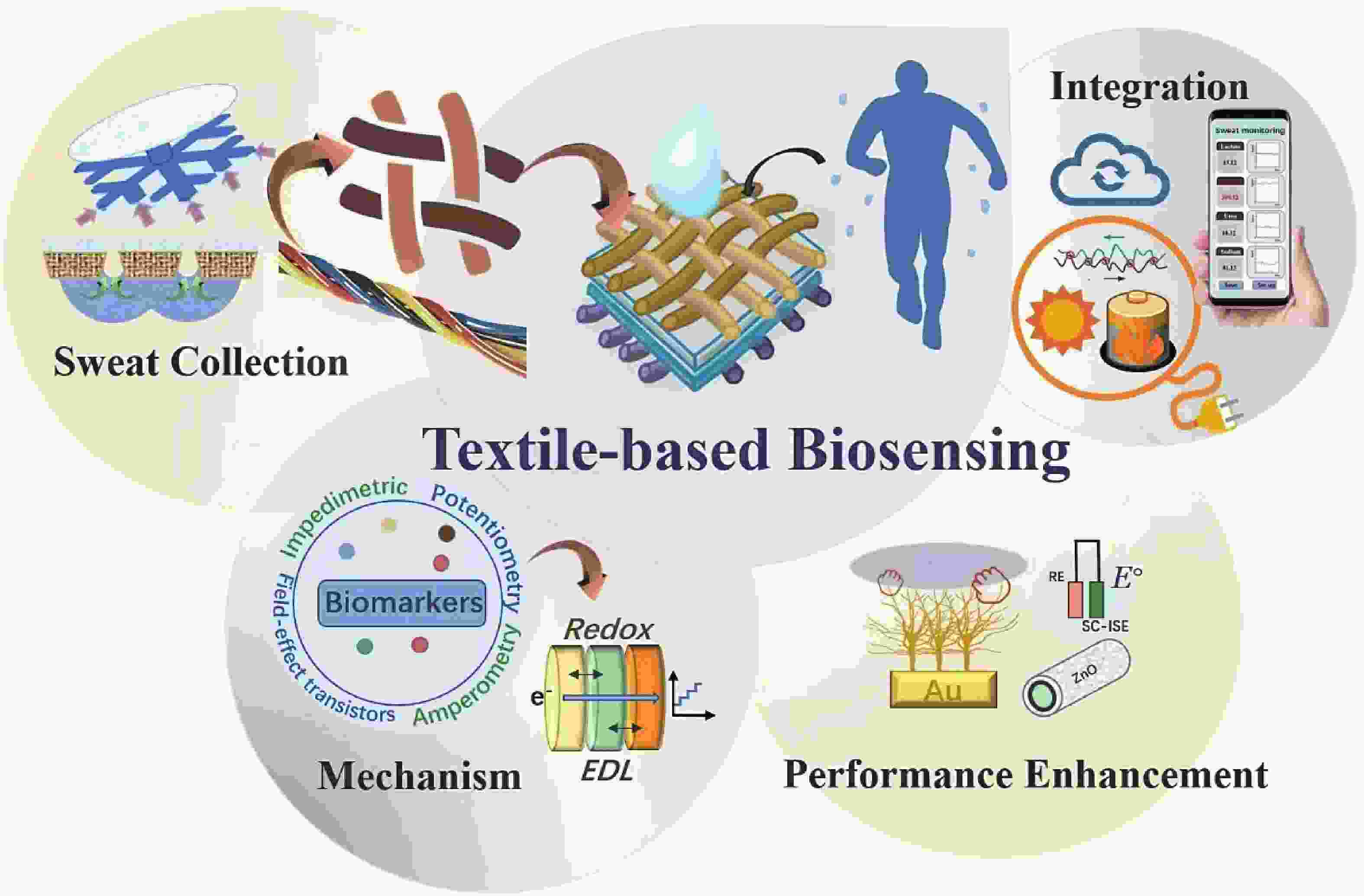
With the rapid technological innovation in materials engineering and device integration, a wide variety of textile-based wearable biosensors have emerged as promising platforms for personalized healthcare, exercise monitoring, and pre-diagnostics. This paper reviews the recent progress in sweat biosensors and sensing systems integrated into textiles for wearable body status monitoring. The mechanisms of biosensors that are commonly adopted for biomarkers analysis are first introduced. The classification, fabrication methods, and applications of textile conductors in different configurations and dimensions are then summarized. Afterward, innovative strategies to achieve efficient sweat collection with textile-based sensing patches are presented, followed by an in-depth discussion on nanoengineering and system integration approaches for the enhancement of sensing performance. Finally, the challenges of textile-based sweat sensing devices associated with the device reusability, washability, stability, and fabrication reproducibility are discussed from the perspective of their practical applications in wearable healthcare.
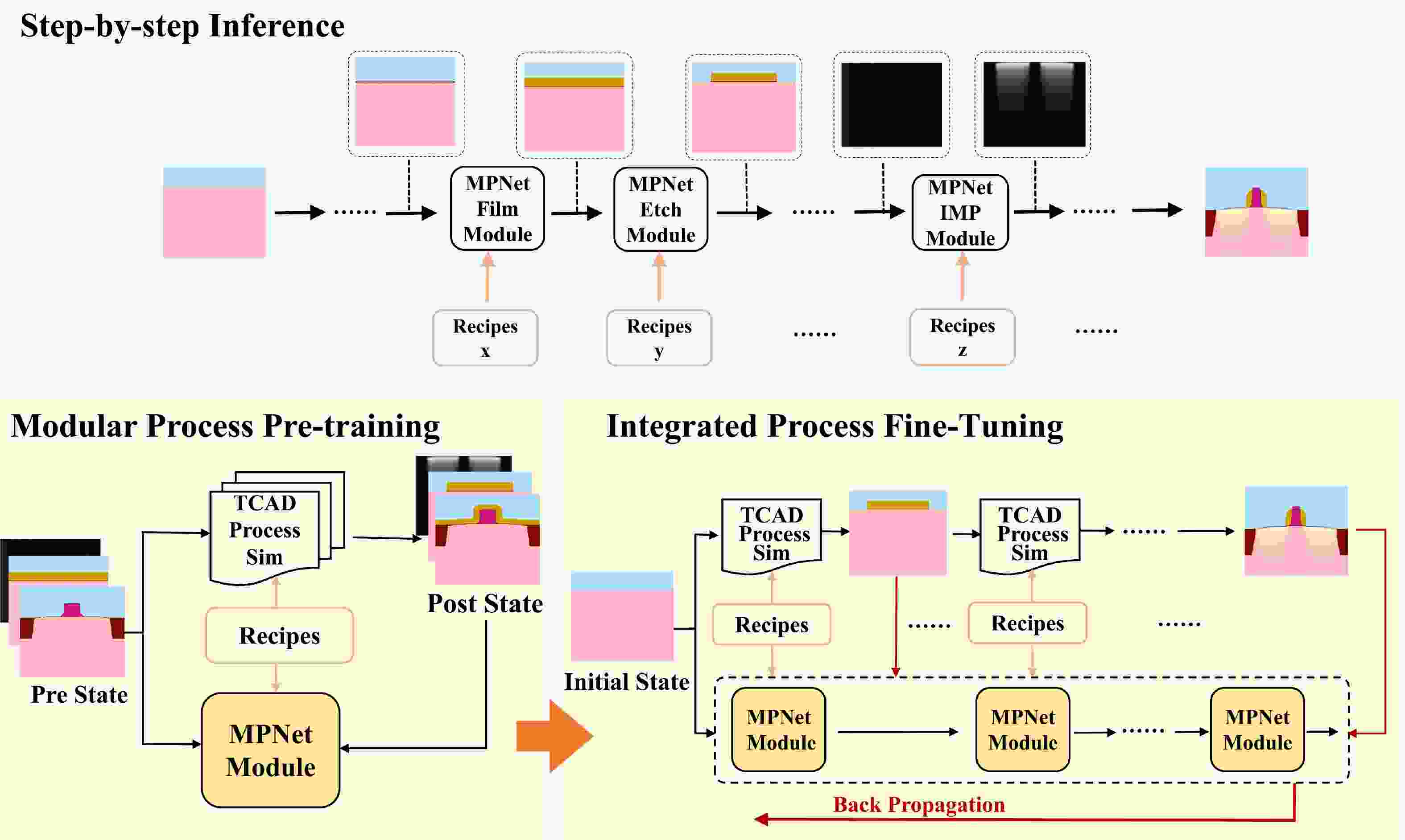
The computational cost of TCAD simulations is becoming prohibitively high with the complexity of advanced process technologies, making simulation acceleration a critical research priority. While end-to-end surrogate models mapping process recipes to device structures and characteristics offer a promising alternative, their application is often limited by poor generalizability and explainability. In this work, we present MPNet, a modular deep learning surrogate modeling framework for process TCAD. MPNet comprises distinct surrogate models for individual process modules, which are assembled into an integrated framework. These modular models employ a novel UNet-attention feature evolution method to capture the complex evolutions of device geometry and doping profiles. Each module can be trained separately on its individual process, after which the modules are cascaded and jointly fine-tuned to minimize error accumulation throughout the cascade. The efficacy of the proposed MPNet framework is demonstrated through a MOSFET integrated process TCAD case study. Results show that MPNet achieves a computational speedup of over 103 times compared to conventional TCAD, while maintaining predictive fidelity exceeding 98%. Finally, to illustrated the application of the proposed framework, MPNet is coupled with a PSO algorithm, showcasing its utility for fast process optimization to meet specific process targets.
Silicon photonics is an emerging competitive solution for next-generation scalable data communications in different application areas as high-speed data communication is constrained by electrical interconnects. Optical interconnects based on silicon photonics can be used in intra/inter-chip interconnects, board-to-board interconnects, short-reach communications in datacenters, supercomputers and long-haul optical transmissions. In this paper, we present an overview of recent progress in silicon optoelectronic devices and optoelectronic integrated circuits(OEICs) based on a complementary metal-oxide-semiconductor-compatible process, and focus on our research contributions. The silicon optoelectronic devices and OEICs show good characteristics, which are expected to benefit several application domains, including communication, sensing, computing and nonlinear systems.


We reported the influence of interface trap density (Nt) on the electrical properties of amorphous InSnZnO based thin-film transistors, which were fabricated at different direct-current (DC) magnetron sputtering powers. The device with the smallest Nt of 5.68 × 1011 cm-2 and low resistivity of 1.21 × 10⁻³ Ω · cm exhibited a turn-on voltage (VON) of -3.60 V, a sub-threshold swing (S.S) of 0.16 V/dec and an on-off ratio (ION/IOFF) of ~ 8 × 10⁸. With increasing Nt, the VON, S.S and ION/IOFF were suppressed to —9.40 V, 0.24 V/dec and 2.59 × 10⁸, respectively. The VTH shift under negative gate bias stress has also been estimated to investigate the electrical stability of the devices. The result showed that the reduction in Nt contributes to an improvement in the electrical properties and stability.

Chemical mechanical polishing (CMP) serves as an indispensable process for achieving global planarization in semiconductor manufacturing, especially as integrated circuit (IC) technology advances to sub-7 nm nodes, where atomic-level surface flatness becomes crucial. Silica abrasives, which account for over 90% of the abrasive market in advanced CMP processes, operate not through simple mechanical grinding but through a key "chemical-mechanical synergistic" mechanism: chemically softening the wafer surface, then mechanically removing the softened layer to expose a new surface, which is further softened and removed, repeating this cycle to produce a smooth wafer. Despite their prevalence, conventional silica abrasives still face challenges, including relatively low material removal rate (MRR), a tendency to agglomerate, leading to poor dispersion and surface defects, and limitations in achieving ultimate surface uniformity. Significant progress has been made to address these issues. Development has progressed from simple spherical particles to complex structural designs (such as mesoporous, hollow, and raspberry-shaped structures) to enhance slurry transport and mechanical action. Surface chemical modifications (e.g., using amino or polymer groups) can improve dispersion stability and reduce scratching. Furthermore, composites with other materials (e.g., ceria, polymers) and precise control of particle size distribution are key to enhancing performance. These innovative approaches have yielded significant performance gains. State-of-the-art slurries have demonstrated the ability to achieve surface roughness below 0.1 nm RMS. The development of silica abrasives is increasingly focused on sustainability and smart manufacturing. A prominent direction is the design of biodegradable abrasives that disintegrate after use, thereby simplifying post-chemical mechanical polishing (CMP) cleanup and minimizing environmental impact—an approach fully aligned with green manufacturing principles. This review systematically summarizes the progress of silica abrasives for CMP over the past 60 years. This summary provides theoretical insights and forward-looking strategies to overcome the current limitations of abrasive technology. We believe this review will be helpful in advancing the field of CMP abrasives towards next-generation semiconductor manufacturing.
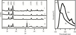
The physical properties and photoelectrochemical characterization of aluminium doped hematite α-Fe2O3, synthesized by spray pyrolysis, have been investigated in regard to solar energy conversion. Stable Al-doped iron (III) oxide thin films synthesized by a spray pyrolysis technique reveals an oxygen deficiency, and the oxide exhibits n-type conductivity confirmed by anodic photocurrent generation. The preparative parameters have been optimized to obtain good quality thin films which are uniform and well adherent to the substrate. The deposited iron oxide thin films show the single hematite phase with polycrystalline rhombohedral crystal structure with crystallite size 20–40 nm. Optical analysis enabled to point out the increase in direct band-gap energy from 2.2 to 2.25 eV with doping concentration which is attributed to a blue shift. The dielectric constant and dielectric loss are studied as a function of frequency. To understand the conduction mechanism in the films, AC conductivity is measured. The conduction occurs by small polaron hopping through mixed valences Fe2+/3+ with an electron mobility 300 K of 1.08 cm2/(V.s). The α-Fe2O3 exhibits long term chemical stability in neutral solution and has been characterized photoelectrochemically to assess its activity as a photoanode for various electrolytes using white light to obtain I–V characteristics. The Al-doped hematite exhibited a higher photocurrent response when compared with undoped films achieving a power conversion efficiency of 2.37% at 10 at% Al:Fe2O3 thin films along with fill factor 0.38 in NaOH electrolyte. The flat band potential Vfb(-0.87 VSCE) is determined by extrapolating the linear part to C-2 = 0 and the slope of the Mott-Schottky plot.

In a recent article, Chen et al. [Electrochimica Acta, 2014, 130: 279] presented their fabrication and characterization results on a graphene/n-Si solar cell where the Au nanoparticles were inserted in graphene to increase its optical and electrical properties. The higher efficiency of the device was attributed to increased conductivity of graphene after doping with Au nanoparticles. However, the knowledge in the field of Schottky diode solar cells relates this to increased band bending at the junction. Also, to explain the instability behaviour, they concluded that the growth of silicon oxide on the Si surface or oxygen adsorption on the window layer resulted in the device performance increasing initially and decreasing in the end. However, this instability seems to be due to variation in series resistance reduced at the beginning because of slightly lowered Fermi level and increased at the end by the self-compensation by deep in-diffusion of Au nanoparticles into n-Si layer. We also propose that inserting a very thin p-type layer at the junction will enhance the carrier collection and performance of this device.
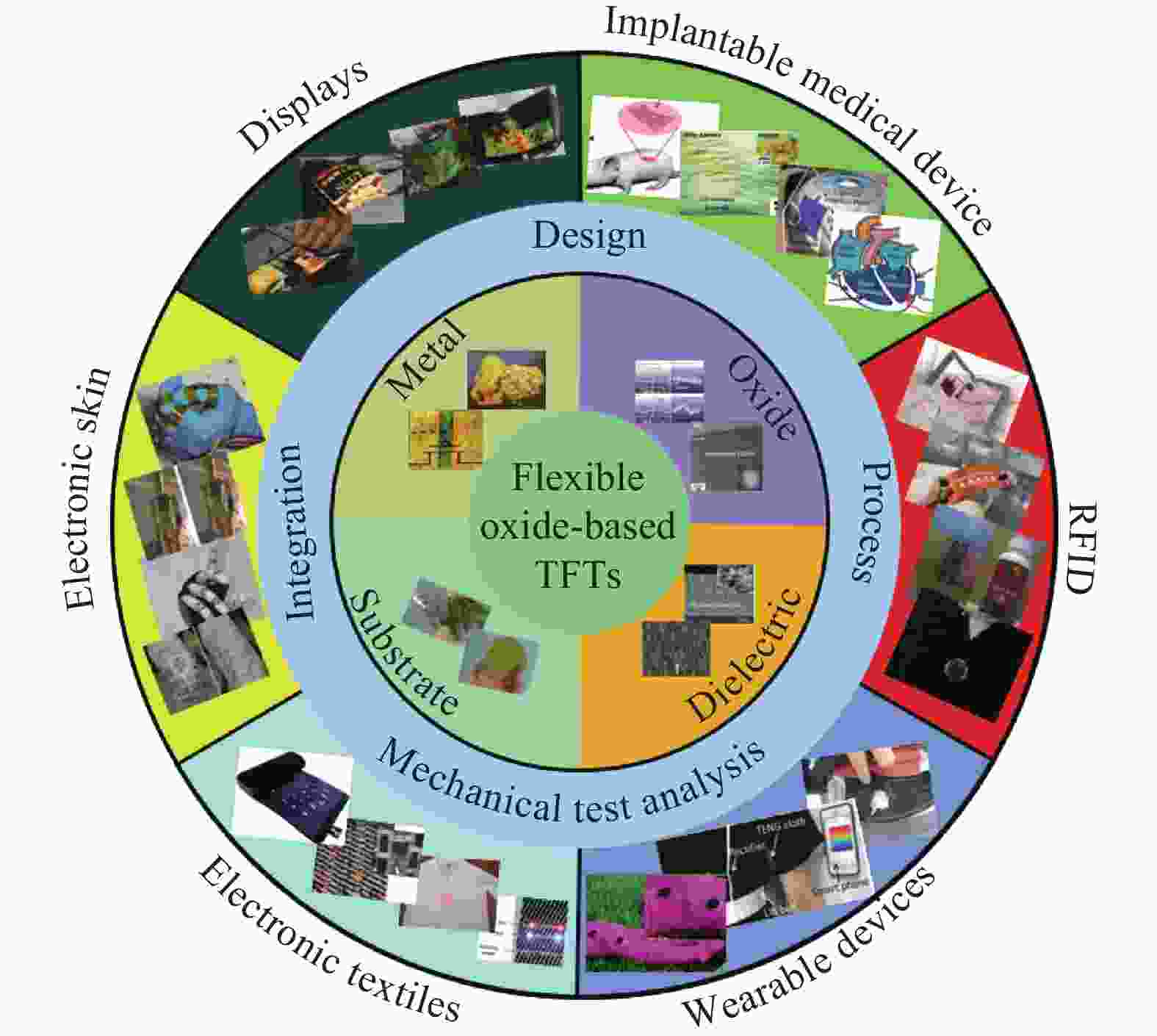
The continuous progress in thin film materials and devices has greatly promoted the development in the field of flexible electronics. As one of the most common thin film devices, thin film transistors (TFTs) are significant building blocks for flexible platforms. Flexible oxide-based TFTs are well compatible with flexible electronic systems due to low process temperature, high carrier mobility, and good uniformity. The present article is a review of the recent progress and major trends in the field of flexible oxide-based thin film transistors. First, an introduction of flexible electronics and flexible oxide-based thin film transistors is given. Next, we introduce oxide semiconductor materials and various flexible oxide-based TFTs classified by substrate materials including polymer plastics, paper sheets, metal foils, and flexible thin glass. Afterwards, applications of flexible oxide-based TFTs including bendable sensors, memories, circuits, and displays are presented. Finally, we give conclusions and a prospect for possible development trends.
The fabrication of zinc oxide (ZnO) from inexpensive solution-processing techniques, namely, electrochemical deposition and electrospinning were explored on various conducting and mesoporous semiconducting surfaces. Optimised conditions were derived for template-and self-assisted nano/micro structures and composites. ZnO thin films were annealed at a fixed temperature under ambient conditions and characterised using physical and optical techniques. The photocurrent response in the UV region shows a fast rise and double decay behaviour with a fast component followed by a slow oscillatory decay. Photocurrent results were correlated with surface chemical analysis from X-ray photoelectron spectroscopy. Various characterisation details reveal the importance of fabrication parameter optimisation for useful low-cost optoelectronic applications.


