Fig. 1.
(Color online) Noise modulation under different modulation orders.
ARTICLES
Guiping Cao and Ning Dong
Corresponding author: Ning Dong, dongning@i-tek.cn
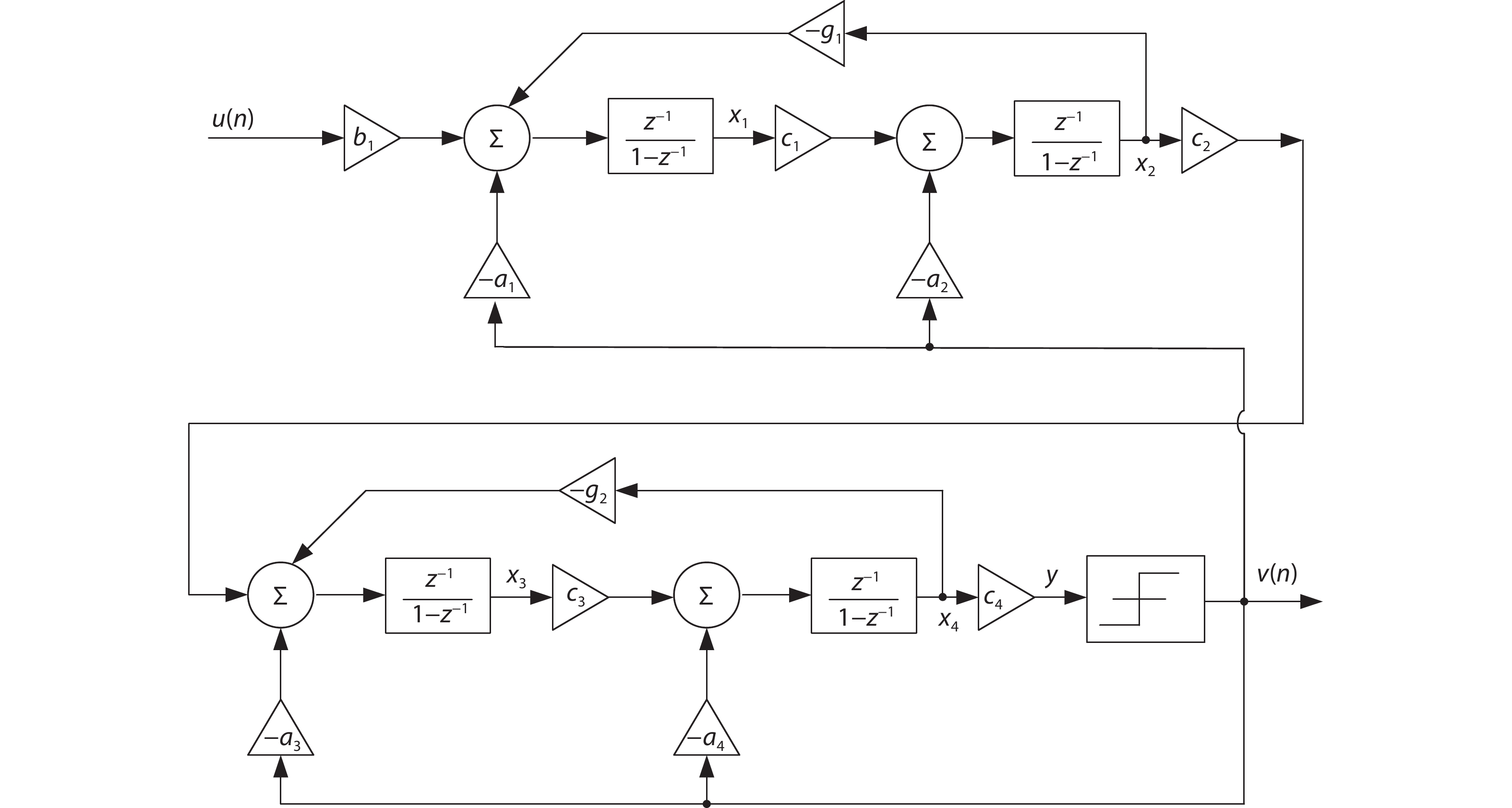
Abstract: Oversampling sigma–delta (Σ–Δ) analog-to-digital converters (ADCs) are currently one of the most widely used architectures for high-resolution ADCs. The rapid development of integrated circuit manufacturing processes has allowed the realization of a high resolution in exchange for speed. Structurally, the Σ–Δ ADC is divided into two parts: a front-end analog modulator and a back-end digital filter. The performance of the front-end analog modulator has a marked influence on the entire Σ–Δ ADC system. In this paper, a 4-order single-loop switched-capacitor modulator with a CIFB (cascade-of-integrators feed-back) structure is proposed. Based on the chosen modulator architecture, the ASIC circuit is implemented using a chartered 0.35 μm CMOS process with a chip area of 1.72 × 0.75 mm2. The chip operates with a 3.3-V power supply and a power dissipation of 22 mW. According to the results, the performance of the designed modulator has been improved compared with a mature industrial chip and the effective number of bits (ENOB) was almost 18-bit.
Key words: sigma–delta modulator, oversampling, CIFB structure, switched-capacitor
| [1] |
Inose H, Inose H, Yasuda Y, et al. A telemetering system by code modulation — Δ–Σ modulation. IRE Trans Space Electron Telemetry, 1962, 8, 204 doi: 10.1109/IRET-SET.1962.5008839
|
| [2] |
Ritchie G R, Candy J, Ninke W. Interpolative digital to analog converters. IEEE Trans Commun, 1974, 22, 1797 doi: 10.1109/TCOM.1974.1092117
|
| [3] |
Candy J C. A use of limit cycle oscillations to obtain robust analog-to-digital converters. IEEE Trans Commun, 1974, 22(3), 298 doi: 10.1109/TCOM.1974.1092194
|
| [4] |
Candy J C, Wooley B, Benjamin O. A voiceband codec with digital filtering. IEEE Trans Commun, 1981, 29(6), 815 doi: 10.1109/TCOM.1981.1095061
|
| [5] |
Candy J C, Benjamin O J. The structure of quantization noise from sigma-delta modulation. IEEE Trans Commun, 1981, 29(9), 1316 doi: 10.1109/TCOM.1981.1095151
|
| [6] |
Candy J C. A use of double integration in sigma-delta modulations. IEEE Trans Commun, 1985, 33(3), 249 doi: 10.1109/TCOM.1985.1096276
|
| [7] |
Candy J C, Huynh A. Double Interpolation for digital-to-analog conversion. IEEE Trans Commun, 1986, 34(1), 77 doi: 10.1109/TCOM.1986.1096428
|
| [8] |
Hayashi T, Inabe Y, Uchimura K, et al. A multistage delta-sigma modulator without double integration loop. ISSCC Digest of Technical Papers, 1986, 182
|
| [9] |
Chen J Q, Ren J Y, Xun J, et al. An 80 dB dynamic range modulator for a GSM system. Chin J Semicond, 2007, 28(2), 294
|
| [10] |
Cao Y, Ren T L, Hong Z L, et al. A 16 bit 96 kHz chopper-stabilized sigma-delta ADC. Chin J Semicond, 2007, 28(8), 1204
|
| [11] |
Yuan J, Zhang Z F, Wu J, et al. Continuous time sigma delta ADC design and non-idealities analysis. J Semicond, 2011, 32(12), 125007 doi: 10.1088/1674-4926/32/12/125007
|
| [12] |
Li R, Li J, Yi T, et al. A 18-mW, 20-MHz bandwidth, 12-bit continuous-time modulator using a power-efficient multi-stage amplifier. J Semicond, 2012, 33(1), 015007 doi: 10.1088/1674-4926/33/1/015007
|
| [13] |
Caldwell T C, Johns D A. An 8-th order MASH delta-sigma with an OSR of 3. ESSCIRC, 2009, 476
|
| [14] |
Chiang J S, Chen H L, Chou P C. A 2.5-V 14-bit MASH sigma-delta modulator for ADSL. IEEE Asia-Pacific Conference on Advanced System Integrated Circuits, 2004, 24
|
| [15] |
Yao L, Steyaert M, Sansen W M. Low-power low-voltage sigma-delta modulators in nanometer CMOS. Springer Science & Business Media, 2006
|
| [16] |
Chao K C, Nadeem S, Lee W L, et al. A higher order topology for interpolative modulators for oversampling A/D converters. IEEE Trans Circuits Syst, 1990, 37(3), 309 doi: 10.1109/31.52724
|
| [17] |
Cao G. Study and ASIC implementation of high-resolution sigma-delta modulator. PhD Thesis, University of Science and Technology of China, 2012
|
| [18] |
Wang F, Harjani R. Power analysis and optimal design of opamps for oversampled converters. IEEE Trans Circuits Syst II, 1999, 46, 359 doi: 10.1109/82.755407
|
| [19] |
Medeiro F, Pérez-Verdú B, de la Rosa J M, et al. Fourth-order cascade SC sigma delta modulator: a comparative study. IEEE Trans Circuits Syst I, 1998, 45(10), 1041 doi: 10.1109/81.728858
|
| [20] |
Ericson M N. High-temperature, high-resolution A/D conversion using 2nd and 4th-order sigma delta modulation in 3.3 V 0.5 µm SOS-CMOS. PhD Thesis, University of Tennessee, 2002
|
| [21] |
Geets Y, Steyaert M, Sansen W. A 2.5 M sample/s multi-bit sigma delta CMOS ADC with 95 dB SN. Digest of Technical Papers, Solid-State Circuits Conference, 2000, 336
|
| [22] |
Balmelli P, Huang Q. A 25 MS/s 14 b 200 mW Σ∆ modulator in 0.18 µm cmos. ISSCC Dig Tech Papers, 2005, 74
|
| [23] |
Brigati S, Francesconi F, Malcovati P, et al. A Fourth-order singla-bit switched capacitor sigma delta modulator for distributed sensor applications. IEEE Trans Instrum Meas, 2004, 53(2), 266 doi: 10.1109/TIM.2003.822480
|
| [24] |
Gerosa A, Neviani A. A 1.8 µW sigma delta modulator for 8-bit digitization of cardiac signals in implantable pacemakers operating down to 1.8 V. IEEE Trans Circuits Syst II, 2005, 52(2), 71 doi: 10.1109/TCSII.2004.840480
|
| [25] |
Yao L, Steyaert M, Sansen W. A 1-V, 1 MS/s, 88-dB sigma delta modulator in 0.13-µm digital CMOS technology. Symposium on VLSI Circuits Digest of Technical, 2005, 180
|
| [26] |
Chen L. High precision Σ∆ ADC. PhD Thesis, Northwestern Polytechnical University, 2006
|
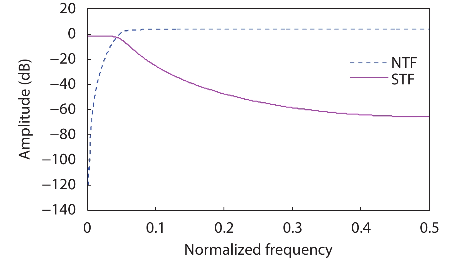
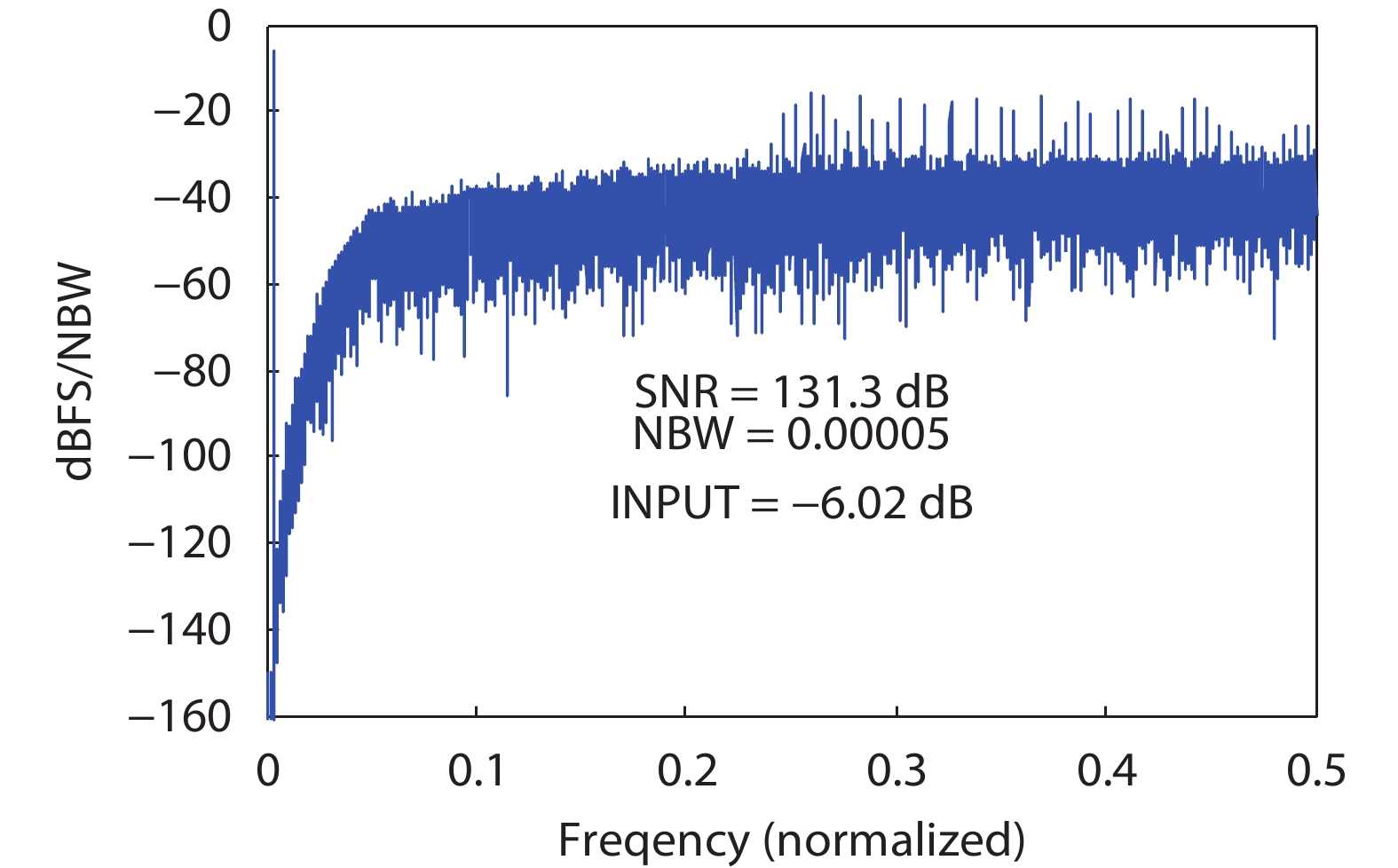
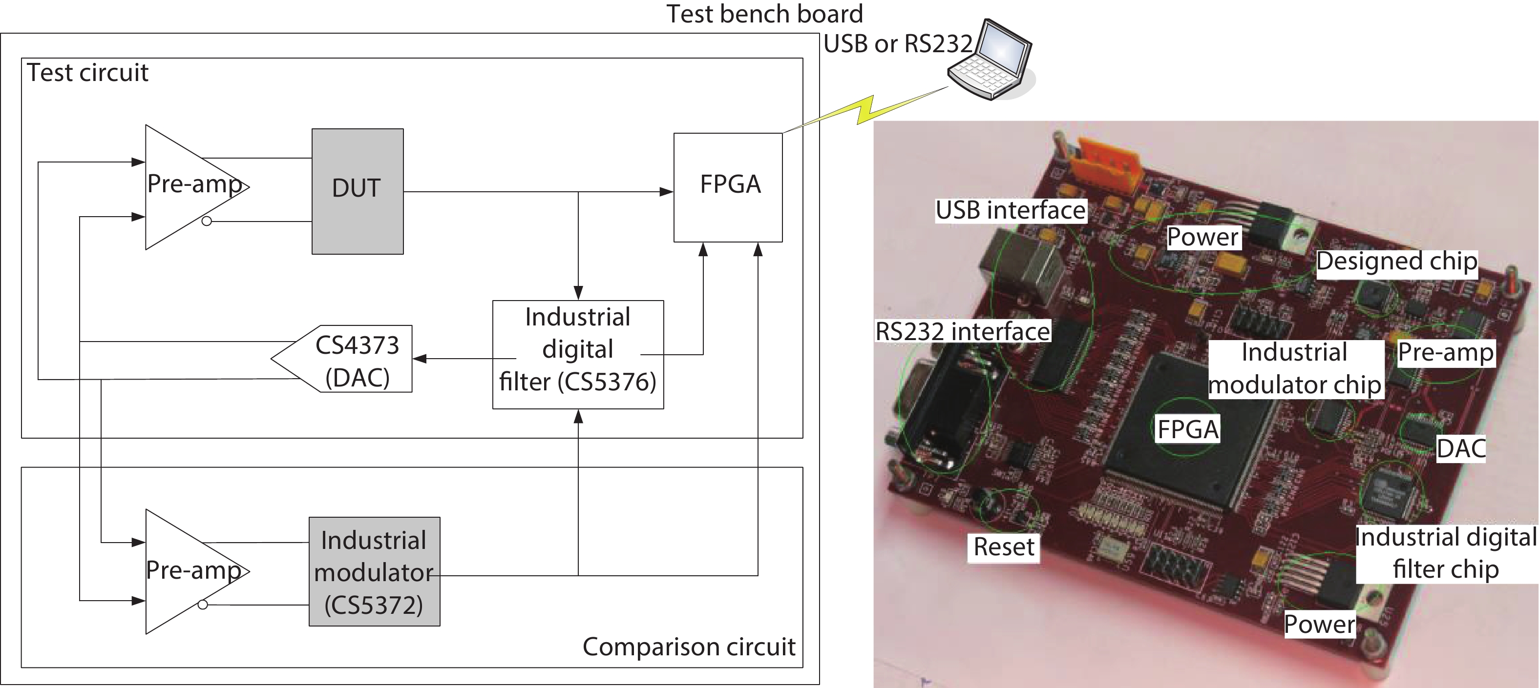
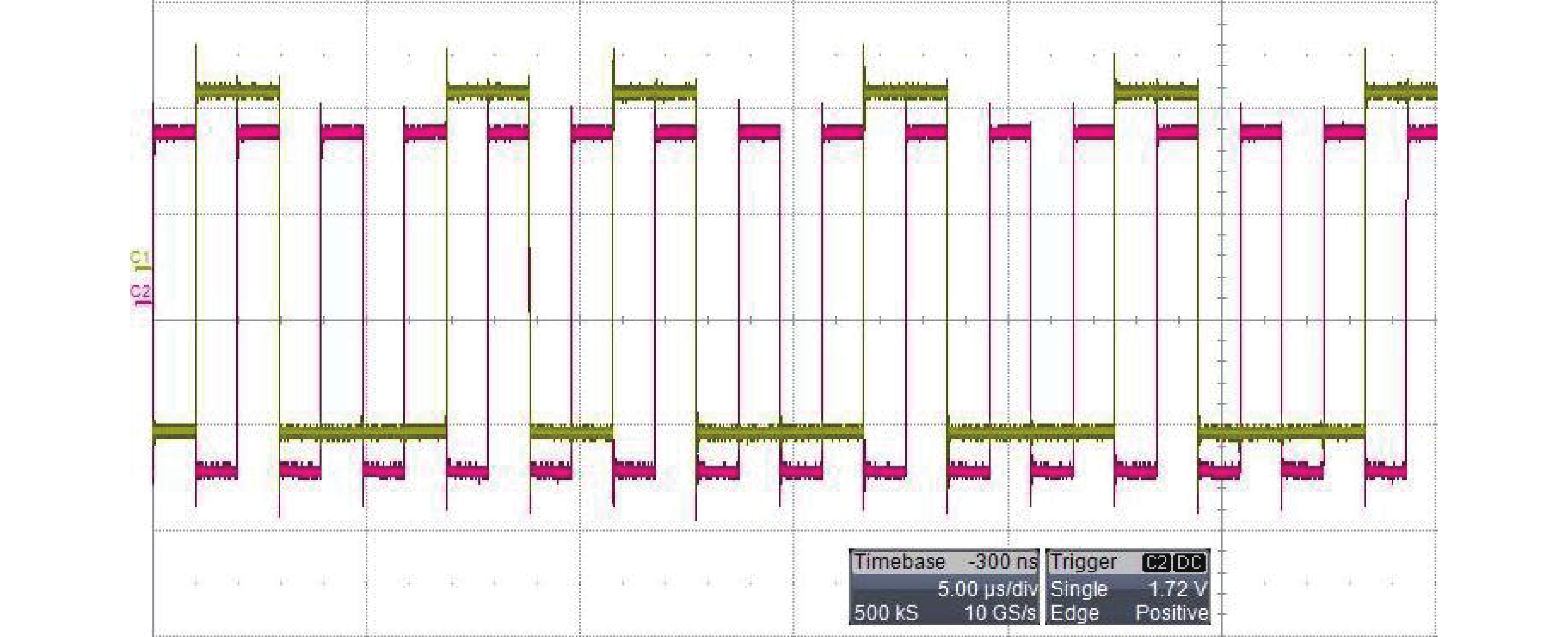
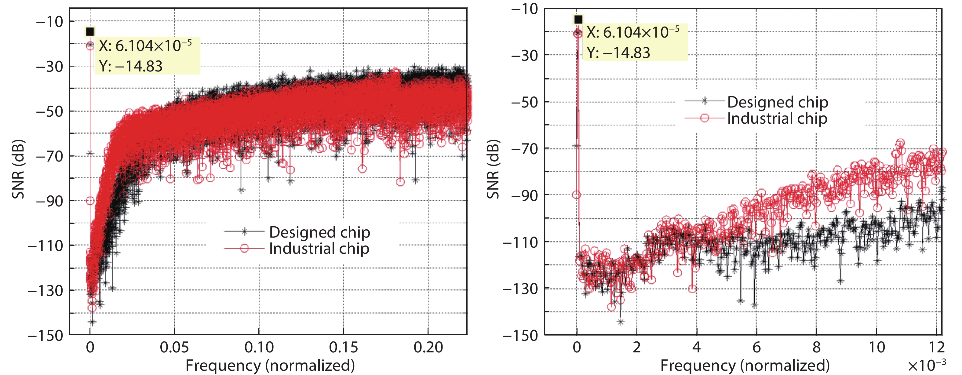

Table 1. CIFB parameters calculated from NTF.
| i | ai | gi | bi | ci |
| 1 | 0.00664 | 0.00007 | 0.0053 | 1 |
| 2 | 0.068261 | 0.00043 | – | 1 |
| 3 | 0.3165 | – | – | 1 |
| 4 | 0.819 | – | – | 1 |
 DownLoad: CSV
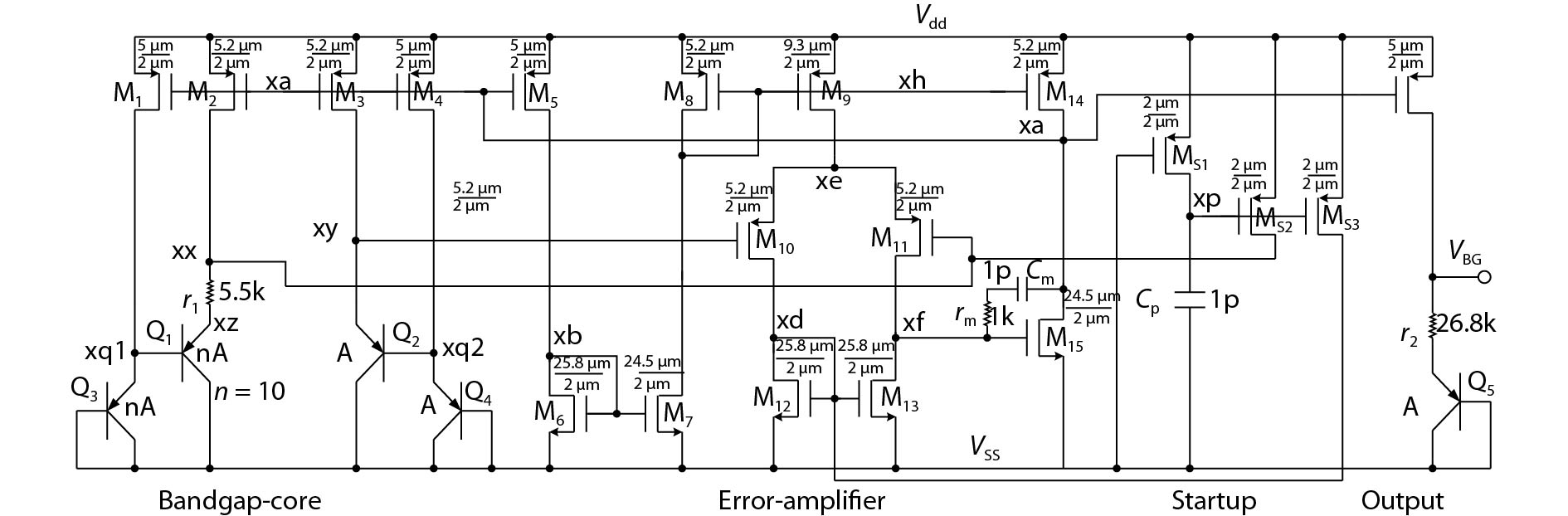
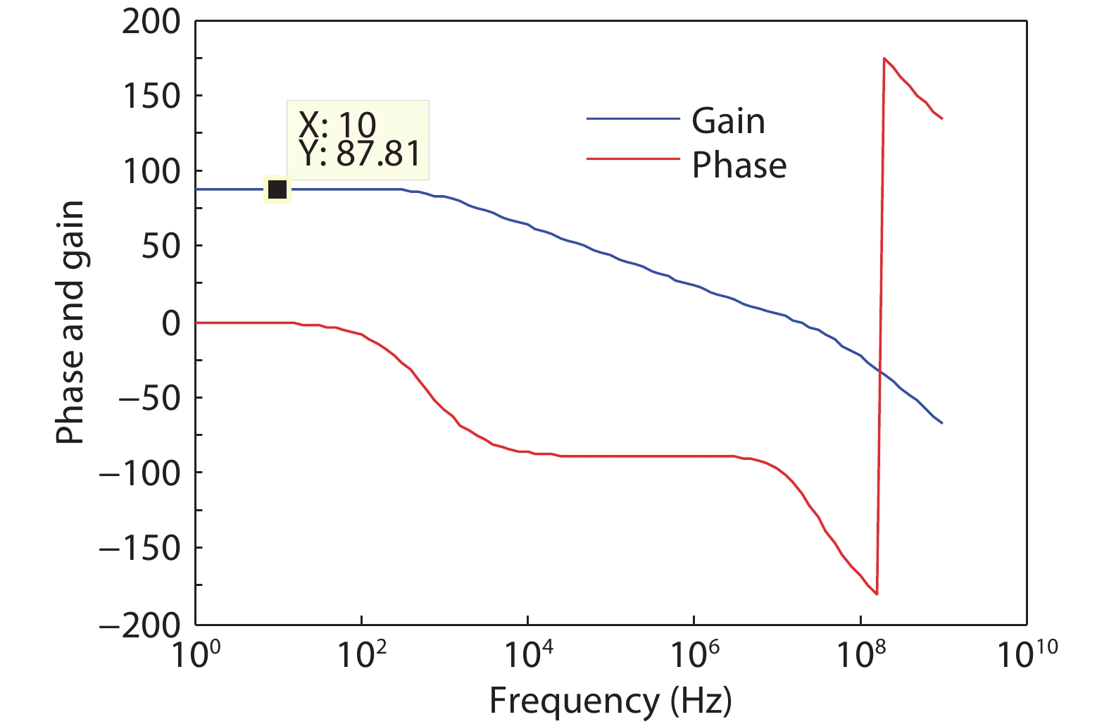
Table 2. Simulation results of OTA.
| DC gain | Phase margin | Power dissipation | GBW | Common offset | Single-side swing | Slew rate | Effective input noise |
| 87.8 dB | 66° | 2.44 mW | 28 MHz | 100 nV | ±2.2 V | 5 V/μs | 14 nV/Hz1/2 (1 kHz) |
DownLoad: CSV
Table 3. Performance comparison between the designed chip and the industrial chip (CS5372).
| Performance | This work | CS5372 |
| SNR (dB) | 93.79 | 93.09 |
| THD (dB) | –101.64 | –102.22 |
| SINAD (dB) | 93.13 dB | 92.59 |
| ENOB (bit) | 15.18 | 15.09 |
| SFDR (dB) | 105.82 | 105.09 |
| ENOB@FS (bit) | 17.65 | 17.56 |
DownLoad: CSV
Table 4. Performance comparison of the Σ–Δ modulators.
| Parameter | ENOB | DOR | Dissipation (mW) | CMOS process (µm) | Power supply (V) | Orders | OSR | Quantizer (bit) | FOM-w |
| Geets[21] | 11.5 | 12.5 Msps | 152 | 0.65 | 5 | 3 | 8 | 1 | 4.20 |
| Balmelli[22] | 13.6 | 2.5 Msps | 200 | 0.18 | 1.8 | 5 | 8 | 4 | 6.44 |
| Brigati[23] | 16.9 | 400 sps | 50 | 0.6 | 5 | 4 | 320 | 1 | 1022.1 |
| Gerosa[24] | 9.1 | 256 sps | 0.0018 | 0.8 | 1.8 | 3 | 16 | 8 | 12.8 |
| Yao[25] | 14.3 | 500 ksps | 7.4 | 0.13 | 1.0 | 4 | 64 | 1 | 0.73 |
| Chen[26] | 12.0 | 48 ksps | 30 | 0.5 | 5 | 5 | 64 | 1 | 8.30 |
| This work | 17.6 | 512 ksps | 22 | 0.35 | 3.3 | 4 | 128 | 1 | 1.63 |
DownLoad: CSV
| [1] |
Inose H, Inose H, Yasuda Y, et al. A telemetering system by code modulation — Δ–Σ modulation. IRE Trans Space Electron Telemetry, 1962, 8, 204 doi: 10.1109/IRET-SET.1962.5008839
|
| [2] |
Ritchie G R, Candy J, Ninke W. Interpolative digital to analog converters. IEEE Trans Commun, 1974, 22, 1797 doi: 10.1109/TCOM.1974.1092117
|
| [3] |
Candy J C. A use of limit cycle oscillations to obtain robust analog-to-digital converters. IEEE Trans Commun, 1974, 22(3), 298 doi: 10.1109/TCOM.1974.1092194
|
| [4] |
Candy J C, Wooley B, Benjamin O. A voiceband codec with digital filtering. IEEE Trans Commun, 1981, 29(6), 815 doi: 10.1109/TCOM.1981.1095061
|
| [5] |
Candy J C, Benjamin O J. The structure of quantization noise from sigma-delta modulation. IEEE Trans Commun, 1981, 29(9), 1316 doi: 10.1109/TCOM.1981.1095151
|
| [6] |
Candy J C. A use of double integration in sigma-delta modulations. IEEE Trans Commun, 1985, 33(3), 249 doi: 10.1109/TCOM.1985.1096276
|
| [7] |
Candy J C, Huynh A. Double Interpolation for digital-to-analog conversion. IEEE Trans Commun, 1986, 34(1), 77 doi: 10.1109/TCOM.1986.1096428
|
| [8] |
Hayashi T, Inabe Y, Uchimura K, et al. A multistage delta-sigma modulator without double integration loop. ISSCC Digest of Technical Papers, 1986, 182
|
| [9] |
Chen J Q, Ren J Y, Xun J, et al. An 80 dB dynamic range modulator for a GSM system. Chin J Semicond, 2007, 28(2), 294
|
| [10] |
Cao Y, Ren T L, Hong Z L, et al. A 16 bit 96 kHz chopper-stabilized sigma-delta ADC. Chin J Semicond, 2007, 28(8), 1204
|
| [11] |
Yuan J, Zhang Z F, Wu J, et al. Continuous time sigma delta ADC design and non-idealities analysis. J Semicond, 2011, 32(12), 125007 doi: 10.1088/1674-4926/32/12/125007
|
| [12] |
Li R, Li J, Yi T, et al. A 18-mW, 20-MHz bandwidth, 12-bit continuous-time modulator using a power-efficient multi-stage amplifier. J Semicond, 2012, 33(1), 015007 doi: 10.1088/1674-4926/33/1/015007
|
| [13] |
Caldwell T C, Johns D A. An 8-th order MASH delta-sigma with an OSR of 3. ESSCIRC, 2009, 476
|
| [14] |
Chiang J S, Chen H L, Chou P C. A 2.5-V 14-bit MASH sigma-delta modulator for ADSL. IEEE Asia-Pacific Conference on Advanced System Integrated Circuits, 2004, 24
|
| [15] |
Yao L, Steyaert M, Sansen W M. Low-power low-voltage sigma-delta modulators in nanometer CMOS. Springer Science & Business Media, 2006
|
| [16] |
Chao K C, Nadeem S, Lee W L, et al. A higher order topology for interpolative modulators for oversampling A/D converters. IEEE Trans Circuits Syst, 1990, 37(3), 309 doi: 10.1109/31.52724
|
| [17] |
Cao G. Study and ASIC implementation of high-resolution sigma-delta modulator. PhD Thesis, University of Science and Technology of China, 2012
|
| [18] |
Wang F, Harjani R. Power analysis and optimal design of opamps for oversampled converters. IEEE Trans Circuits Syst II, 1999, 46, 359 doi: 10.1109/82.755407
|
| [19] |
Medeiro F, Pérez-Verdú B, de la Rosa J M, et al. Fourth-order cascade SC sigma delta modulator: a comparative study. IEEE Trans Circuits Syst I, 1998, 45(10), 1041 doi: 10.1109/81.728858
|
| [20] |
Ericson M N. High-temperature, high-resolution A/D conversion using 2nd and 4th-order sigma delta modulation in 3.3 V 0.5 µm SOS-CMOS. PhD Thesis, University of Tennessee, 2002
|
| [21] |
Geets Y, Steyaert M, Sansen W. A 2.5 M sample/s multi-bit sigma delta CMOS ADC with 95 dB SN. Digest of Technical Papers, Solid-State Circuits Conference, 2000, 336
|
| [22] |
Balmelli P, Huang Q. A 25 MS/s 14 b 200 mW Σ∆ modulator in 0.18 µm cmos. ISSCC Dig Tech Papers, 2005, 74
|
| [23] |
Brigati S, Francesconi F, Malcovati P, et al. A Fourth-order singla-bit switched capacitor sigma delta modulator for distributed sensor applications. IEEE Trans Instrum Meas, 2004, 53(2), 266 doi: 10.1109/TIM.2003.822480
|
| [24] |
Gerosa A, Neviani A. A 1.8 µW sigma delta modulator for 8-bit digitization of cardiac signals in implantable pacemakers operating down to 1.8 V. IEEE Trans Circuits Syst II, 2005, 52(2), 71 doi: 10.1109/TCSII.2004.840480
|
| [25] |
Yao L, Steyaert M, Sansen W. A 1-V, 1 MS/s, 88-dB sigma delta modulator in 0.13-µm digital CMOS technology. Symposium on VLSI Circuits Digest of Technical, 2005, 180
|
| [26] |
Chen L. High precision Σ∆ ADC. PhD Thesis, Northwestern Polytechnical University, 2006
|


Article views: 7046 Times PDF downloads: 282 Times Cited by: 0 Times
Received: 25 October 2019 Revised: 08 December 2019 Online: Accepted Manuscript: 24 February 2020Uncorrected proof: 05 March 2020Published: 01 June 2020
| Citation: |
Guiping Cao, Ning Dong. An 18-bit sigma –delta switched-capacitor modulator using 4-order single-loop CIFB architecture[J]. Journal of Semiconductors, 2020, 41(6): 062404. doi: 10.1088/1674-4926/41/6/062404
****
G P Cao, N Dong, An 18-bit sigma –delta switched-capacitor modulator using 4-order single-loop CIFB architecture[J]. J. Semicond., 2020, 41(6): 062404. doi: 10.1088/1674-4926/41/6/062404.

|
| [1] |
Inose H, Inose H, Yasuda Y, et al. A telemetering system by code modulation — Δ–Σ modulation. IRE Trans Space Electron Telemetry, 1962, 8, 204 doi: 10.1109/IRET-SET.1962.5008839
|
| [2] |
Ritchie G R, Candy J, Ninke W. Interpolative digital to analog converters. IEEE Trans Commun, 1974, 22, 1797 doi: 10.1109/TCOM.1974.1092117
|
| [3] |
Candy J C. A use of limit cycle oscillations to obtain robust analog-to-digital converters. IEEE Trans Commun, 1974, 22(3), 298 doi: 10.1109/TCOM.1974.1092194
|
| [4] |
Candy J C, Wooley B, Benjamin O. A voiceband codec with digital filtering. IEEE Trans Commun, 1981, 29(6), 815 doi: 10.1109/TCOM.1981.1095061
|
| [5] |
Candy J C, Benjamin O J. The structure of quantization noise from sigma-delta modulation. IEEE Trans Commun, 1981, 29(9), 1316 doi: 10.1109/TCOM.1981.1095151
|
| [6] |
Candy J C. A use of double integration in sigma-delta modulations. IEEE Trans Commun, 1985, 33(3), 249 doi: 10.1109/TCOM.1985.1096276
|
| [7] |
Candy J C, Huynh A. Double Interpolation for digital-to-analog conversion. IEEE Trans Commun, 1986, 34(1), 77 doi: 10.1109/TCOM.1986.1096428
|
| [8] |
Hayashi T, Inabe Y, Uchimura K, et al. A multistage delta-sigma modulator without double integration loop. ISSCC Digest of Technical Papers, 1986, 182
|
| [9] |
Chen J Q, Ren J Y, Xun J, et al. An 80 dB dynamic range modulator for a GSM system. Chin J Semicond, 2007, 28(2), 294
|
| [10] |
Cao Y, Ren T L, Hong Z L, et al. A 16 bit 96 kHz chopper-stabilized sigma-delta ADC. Chin J Semicond, 2007, 28(8), 1204
|
| [11] |
Yuan J, Zhang Z F, Wu J, et al. Continuous time sigma delta ADC design and non-idealities analysis. J Semicond, 2011, 32(12), 125007 doi: 10.1088/1674-4926/32/12/125007
|
| [12] |
Li R, Li J, Yi T, et al. A 18-mW, 20-MHz bandwidth, 12-bit continuous-time modulator using a power-efficient multi-stage amplifier. J Semicond, 2012, 33(1), 015007 doi: 10.1088/1674-4926/33/1/015007
|
| [13] |
Caldwell T C, Johns D A. An 8-th order MASH delta-sigma with an OSR of 3. ESSCIRC, 2009, 476
|
| [14] |
Chiang J S, Chen H L, Chou P C. A 2.5-V 14-bit MASH sigma-delta modulator for ADSL. IEEE Asia-Pacific Conference on Advanced System Integrated Circuits, 2004, 24
|
| [15] |
Yao L, Steyaert M, Sansen W M. Low-power low-voltage sigma-delta modulators in nanometer CMOS. Springer Science & Business Media, 2006
|
| [16] |
Chao K C, Nadeem S, Lee W L, et al. A higher order topology for interpolative modulators for oversampling A/D converters. IEEE Trans Circuits Syst, 1990, 37(3), 309 doi: 10.1109/31.52724
|
| [17] |
Cao G. Study and ASIC implementation of high-resolution sigma-delta modulator. PhD Thesis, University of Science and Technology of China, 2012
|
| [18] |
Wang F, Harjani R. Power analysis and optimal design of opamps for oversampled converters. IEEE Trans Circuits Syst II, 1999, 46, 359 doi: 10.1109/82.755407
|
| [19] |
Medeiro F, Pérez-Verdú B, de la Rosa J M, et al. Fourth-order cascade SC sigma delta modulator: a comparative study. IEEE Trans Circuits Syst I, 1998, 45(10), 1041 doi: 10.1109/81.728858
|
| [20] |
Ericson M N. High-temperature, high-resolution A/D conversion using 2nd and 4th-order sigma delta modulation in 3.3 V 0.5 µm SOS-CMOS. PhD Thesis, University of Tennessee, 2002
|
| [21] |
Geets Y, Steyaert M, Sansen W. A 2.5 M sample/s multi-bit sigma delta CMOS ADC with 95 dB SN. Digest of Technical Papers, Solid-State Circuits Conference, 2000, 336
|
| [22] |
Balmelli P, Huang Q. A 25 MS/s 14 b 200 mW Σ∆ modulator in 0.18 µm cmos. ISSCC Dig Tech Papers, 2005, 74
|
| [23] |
Brigati S, Francesconi F, Malcovati P, et al. A Fourth-order singla-bit switched capacitor sigma delta modulator for distributed sensor applications. IEEE Trans Instrum Meas, 2004, 53(2), 266 doi: 10.1109/TIM.2003.822480
|
| [24] |
Gerosa A, Neviani A. A 1.8 µW sigma delta modulator for 8-bit digitization of cardiac signals in implantable pacemakers operating down to 1.8 V. IEEE Trans Circuits Syst II, 2005, 52(2), 71 doi: 10.1109/TCSII.2004.840480
|
| [25] |
Yao L, Steyaert M, Sansen W. A 1-V, 1 MS/s, 88-dB sigma delta modulator in 0.13-µm digital CMOS technology. Symposium on VLSI Circuits Digest of Technical, 2005, 180
|
| [26] |
Chen L. High precision Σ∆ ADC. PhD Thesis, Northwestern Polytechnical University, 2006
|

 WeChat ID
Journal of Semiconductors © 2017 All Rights Reserved 京ICP备05085259号-2