1. Departments of Applied Physics, Xi'an University of Technology, Xi'an 710048, ChinaDepartments of Applied Physics, Xi'an University of Technology, Xi'an 710048, China
2. Institute of Physics and Electronic Engineering, Xinjiang Normal University, Urumqi 830054, ChinaInstitute of Physics and Electronic Engineering, Xinjiang Normal University, Urumqi 830054, China
Abstract: Experiments with the limited space-charge accumulation (LSA) mode of oscillation in a large gap semi-insulating (SI) GaAs photoconductive semiconductor switch (PCSS) are discussed. It has been observed that growth and drift of a photo-activated charge domain (PACD) are quenched only when the bias voltage is more than twice the threshold voltage. The original negative resistance characteristics are directly utilized in the LSA mode; during LSA operation the spatial average of the electric field varies over a large portion of the negative differential mobility region of the velocity-electric field characteristic. The work efficiency of an SI GaAs PCSS is remarkably enhanced by electric field excursions into the positive resistance region when the total electric field is only below the threshold part of the time. The LSA mode can only operate in the certain conditions that satisfy the quenching of the accumulation layer and the smaller initial domain voltage.
Photoconductive semiconductor switches (PCSSs) have many advantages, such as high power, fast switching speed, small parasitic capacitance, high repetition frequency, and being jitter-free. Therefore they show a broad application prospect in the fields of superspeed electronics, high power electrical pulses generation, fine-synchronization control, and terahertz technology[1-4]. In 1982, the linear photoconduction working mode was investigated in semi-insulating semiconductors by Willamson[5]. In 1987, Loubriel discovered the high gain mode (which is also called lock-on or nonlinear mode) in a GaAs chip[6]. A number of subsequent experimental studies indicated that the nonlinear mode of SI GaAs PCSSs have some typical characteristics[7, 8]. In general, the two working modes are mutually non-correlated[9-11]. The generation of microwave power from a bulk GaAs sample operating in limited space-charge accumulation (LSA) mode is discussed in Ref.[12]. Copeland published his theoretical explanation of the LSA mode with experimental verification; this mode has made it possible for solid-state devices to not be limited by the transit time of the charge carriers through the device[13, 14]. Curtice indicated that the LSA mode should be more easily obtainable in long GaAs devices at high bias values since the operating requirements are less restrictive[15]; the most important effect at high bias level is the reduction in dipole domain growth. The steady-state and transient characteristics in high-field dipole domains in a long GaAs Gunn diode have been tested and analyzed, and then the current response of devices was found following a step function of the applied voltage while a domain is in transit in the manner first proposed by Kuru in Ref.[16]. Late in 1972, Jones indicated that strict dipole domain modes in devices are less significant than might be guessed from the known behaviors of long GaAs samples by inference[17], and operating characteristics for overlength mode of InP transferred-electron devices are investigated[18]. Terahertz generation in the limited space-charge accumulation is studied by Kim et al.for nanoscale GaN diodes[19, 20]. The generation of power at terahertz frequencies is analyzed by Wickenden for a single-walled semiconducting carbon nanotube, they consider the regime of limited-space-charge accumulation within nanotubes[21]. The device must be long enough for accumulation layer transit from the cathode not to appreciably distort the electric field uniformity[22, 23]. This mode of operation offers some advantages over the Gunn mode, in the first place the frequency of operation is no longer linked with the transition time to some extent; as a result operation at high frequencies becomes much easier; further, since there is no domain nucleation the source should be less noisy; thirdly the efficiency should be higher than other Gunn effect device modes. The PACD is formed successively so that the oscillation frequency is approximately equal to the carrier drift velocity divided by the chip in an SI GaAs PCSS[24]. We found that by using an external resonant circuit coupled to an appropriate PCSS, a new mode of operation can be attained which utilizes the entire length of the chip to give coherent oscillations, the frequency of which does not depend on sample length, which is larger than a limited value. Hence, by using a relatively large gap switch, both high frequency and efficient high power operation can be obtained. The LSA mode of the GaAs PCSS is first verified in the experiment results in Refs. [25, 26]. In this paper, we report the initial experiments results and the peculiar transmission characteristics for large gap SI GaAs PCSSs at high bias voltage. These switches in experiment do not appear to have typical nonlinear phenomena at high bias voltage, but show a stable linear status. The large gap SI GaAs PCSS we develop operates in the LSA mode when the switch satisfies the conditions of accumulation layer formation is the product of the carrier and length of switch gap satisfies n0l⩾ 1013 cm−2; a ratio of carrier concentration and frequency n0/f⩽ 3 × 10⁵ s/cm3 must be met for inhibition accumulation, and n0/f⩾ 5 × 10⁴ s/cm3 can ensure that the accumulated space charge is completely dissipated. The peculiar working mode can effectively control space charge to improve withstand voltage properties, service life is significantly enhanced, and the switch can be protected from damage at high bias voltage, as well as other advantages. Experiments with the LSA mode of operating characteristics in a large gap SI GaAs PCSS are also discussed in this paper.
2.
Experimental setup and results
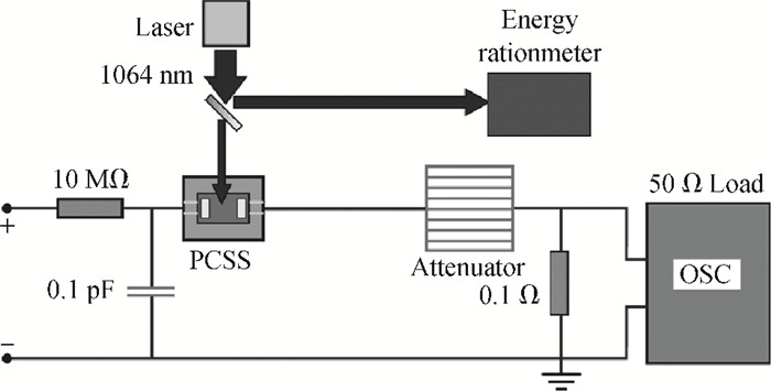
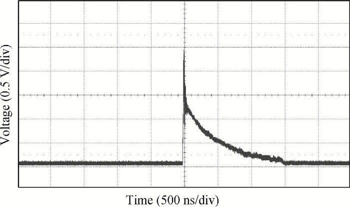
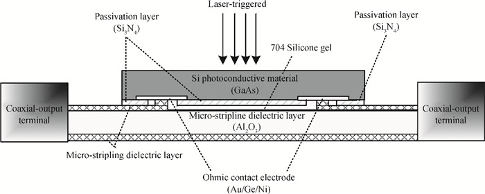
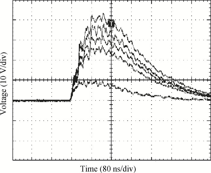
In our experiment, the photoconductive material used for the PCSS was SI GaAs with the unintentionally doped impurity concentration of 1.5 × 107 cm−3. The resistivity in total darkness was larger than 5 × 10⁷Ω⋅cm, and the mobility was larger than 5500 cm2/(V⋅s). The overall size of the GaAs wafer was 5 mm wide × 4 mm long × 0.6 mm thick. Using the electron beam evaporation technique, a Au/Ge/Ni alloy electrode forms an ohmic contact by using a standard mixture of Ni/Au-Ge/Au for the metallization at 450 ℃, and the thickness is 700 nm. The electrode dimensions were 8 × 3 mm2, and the gap between the two electrodes was 4 mm, the schematic of the lateral PCSS is illustrated in Fig. 1. The GaAs chip had a pair of substantially ohmic connections spaced apart along the chip and was placed on the copper clad board with a transmission line, and the transmission line was connected with two coaxial connectors. The test circuit for high-voltage, high-current PCSS experiments is shown in Fig. 2, a high-voltage power supply charged capacitor (0.1 pF) and a 10 MΩ resistor was used to limit the current, the capacitor provided a bias voltage to the PCSS. The laser type in experiment was a neodymium-doped YAG SUNlite-20 laser, pulse width was 500 ps, wavelength was 1064 nm and triggered light energy was 1 mJ. An energy meter KSDP2210-CAS-1 was used to measure the laser energy. The storage oscilloscope was a Lecory-8600A Wave Master. A 60 dB coaxial attenuator with a power of 200W was used between the 0.1 Ω resistance and the oscilloscope. Superposed output waveforms triggered 100 times continuously appeared at 3300 V bias voltage, as shown in Fig. 3, output waveforms appeared the typical lock-on characteristics.
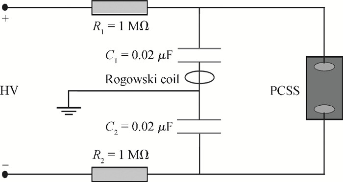
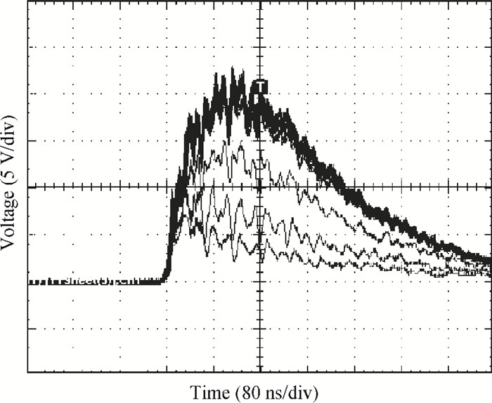
The material and characteristic of chip in the large gap SI GaAs PCSS is essentially the same as the above experiment, switches of two kinds of electrode gap are making experimental testing respectively. The test circuit is shown in Fig. 4, the PCSS was charged by two series-wound capacitors, and the two capacitors were connected with DC high voltage electrical source through two water electric resistances, respectively. The light source used to excite the PCSS was a neodymium-doped YAG nanosecond laser that produced a 15 ns full width at half maximum laser pulse at 1064 nm wavelength. Currents through the PCSS were measured with a Rogowski coil, whose sensitivity and minimum response time were 0.1 V/A and 1 ns. The storage oscilloscope used was TDS-5054. These typical linear output electrical pulses of the 12 mm gap PCSS at the bias voltages of 6.6, 16, 20, 24, and 26 kV from the bottom to up and laser energy about 8 mJ are displayed in Fig. 5. The output waveforms of the 14 mm gap switch exhibit a series linear characteristic at the bias voltages of 6.4, 10, 12, and 20 kV (triggered continuous 20) from the bottom to up in Fig. 6.
Figure
4.
Circuit diagram for the gap SI-GaAs PCSS.
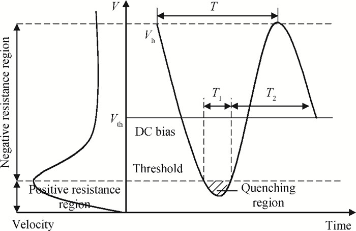
It is well known that negative differential behavior is a result of the conduction band structure of GaAs. Transferred electron devices utilize a relationship between the mean electron drift velocity and the electric field of the form shows in Fig. 7 (the (v, E) relationship) with a region of negative differential mobility. The number of electrons transferred from the high to low mobility state becomes a sensitive function of electric field above a threshold 3 kV/cm and a negative differential mobility occurs in GaAs. There is a finite time for electrons to be accelerated or decelerated following a change of field (the energy relaxation time) and a finite time for transfer between mobility states (the intervalley scattering time), both of which contribute to an upper frequency. Copeland pointed out that if a GaAs sample was operated well above the threshold field in a resonant circuit of high impedance, the microwave field could be large enough to swing the resultant field below the threshold for a part of each cycle in Fig. 7[27]. The time the device is held below threshold can be long enough for any incipient domains to be quenched, for below the threshold field the dielectric relaxation time is positive. Domains start to grow again when the field rises above threshold, but if the time above threshold is shorter than the negative dielectric relaxation time any accumulation of space charge will be severely limited. The LSA mode can only operate if certain conditions are observed relating frequency to the negative and positive dielectric relaxation times. Localized electron accumulations grow instead of dispersing as in a positive differential mobility medium and travel at a velocity similar to the post-threshold electron drift velocities. Temporal control of space charge in a body effect device is possible in the LSA mode. The instantaneous current-voltage relationship follows the (v, E) characteristic and operation approaches that of a large signal negative resistor without transit time limitation.
Figure
7.
Operating principle of the LSA mode[27].
The LSA mode can only operate if certain conditions are relating frequency to the negative and positive dielectric relaxation times in the large gap SI GaAs PCSS. The switch is characterized by a negative resistance when subjected to voltages within a voltage range above a predetermined threshold voltage, an inherent traveling domain frequency when subjected to only a direct current voltage which is within voltage range, and a product of carrier concentration n0 and chip length l at least twice the minimum value required for permitting the formation of traveling domains[28,29]. Obviously, in order for space-charge instabilities to occur, the total growth factor must be large in comparison with unit value in an SI GaAs PCSS. This means the product of n0 and l must satisfy the inequality n0l⩾ 1013 cm−2; when this requirement is not satisfied, the formation of strong space-charge instabilities should not be expected. If the circuit frequency is adequately higher than the transit-time frequency, the n0l product need not necessarily be kept close to 1012 electrons per square centimeter in order to prevent the formation of domains. The LSA mode will only exist if the domain voltage can be kept small throughout the cycle. As can be seen, large values of initial domain voltage will not allow the LSA mode to exist. The conditions of the accumulation layer quenching and cyclic operation occur if the domain voltage decays to a value equal to the initial domain voltage during the period that the anode field is below the threshold determining whether the LSA mode for SI GaAs PCSS can be sustained. Space-charge growth is determined by negative dielectric relaxation time τR=ε/enμ′, where ε is the permittivity of the sample, μ′ is the mobility of SI GaAs material, e is the charge of an electron, and n is the density of carriers and approximately equal to n0 due to space-charge accumulation is very small in the LSA. The main influencing factors is positive dielectric relaxation time for LSA mode in SI GaAs PCSS, the accumulated space charge must be all dissipated with dielectric relaxation behavior; the switch rapidly transforms from the accumulation stage to the LSA stage.
We have shown that the proper operating condition of a ratio of carrier concentration and frequency n0/f⩽ 3 × 10⁵ s/cm3 must be met for inhibition accumulation, and n0/f⩾ 5 × 10⁴ s/cm3 can ensure that the accumulated space charge must be dissipated completely. The large gap SI GaAs PCSS operates on the principle that the bulk negative resistance of the PCSS can be used to produce AC power without forming frequency-limiting traveling domains if the relevant parameters are arranged so that electric fields in the material oscillate between the positive resistance and negative resistance regions of the sample with the excursions into the negative resistance region being sufficiently short that space-charge accumulations associated with PACD do not have time to form. However, these time excursions into the negative resistance region are also sufficiently long with respect to the time in which the electric field extends into the positive resistance region. The ratio of the negative resistance portion of each cycle to the positive resistance portion is sufficiently small to prevent the formation of traveling domain oscillations in the SI GaAs PCSS. Figure 7 is a graph of electron velocity versus electric field (this is negative resistance characteristic) in the GaAs material and a graph of electric field versus time in LSA mode. The amplitude and frequency of the oscillating field E is arranged so that during an interval T1 of each cycle it drops below the threshold voltage into the positive resistance region, and during another interval T2, it is higher than Eth and therefore extends into the negative resistance region. During interval T2 the PCSS delivers AC power into the tank circuit and during T1 it dissipates AC power due to the positive resistance. By assuring a higher gain in energy during T2 than the loss during T1, a net gain is attained and the oscillations are sustained by the switch. Traveling PACD oscillation is precluded by making the electric field rise from below the threshold Eth to a high value and back below Eth so quickly that the space-charge distribution throughout the chip associated with PACD does not have time to form. A space-charge accumulation layer will form due to electron injection from the cathode contact, but since the field E is in the negative resistance region for less time than is necessary for space-charge growth, no appreciable depletion layer can form and the field E throughout most of the chip remains in the negative resistance region above Eth. Secondly, the time interval T1 in the positive resistance region is made sufficiently long to dissipate substantially the space-charge accumulation layer that forms. It can further be shown that, in order to quench a single accumulation layer, it is not necessary to reduce the field to that point at which PACD would become quenched. Instead, it is sufficient to reduce the field only somewhat below the threshold field of the velocity-field characteristic. This is because the field difference across a primary accumulation layer is much weaker than the field differences that build up in a mature PACD to making the primary accumulation layer easier to quench. The LSA mode for different sample lengths of GaAs device was comparatively studied in Refs. [22, 23], drawing conclusions from experiments in which the sample length is much more than the distance between anode and accumulation layer, and the distance of accumulation layer traveling in a long sample is much smaller than a short sample under certain conditions. So growth and drift of PACD can be suppressed efficiently by the long chip and the LSA mode is easier to operate in the large gap SI GaAs PCSS in a strong bias field. To improve the LSA mode, there are restrictions as to uniformity of GaAs material and internal field in an SI GaAs PCSS; these conditions are depend not only on pure material and good device technology but also an appropriate external circuit.
4.
Conclusion
Our descriptions have now shown how the LSA mode in SI GaAs PCSS is achieved, namely, by periodic quenching of the primary accumulation layer that detaches itself from the cathode during every cycle. The conditions of the accumulation layer quenching and cyclic operation occurring if the domain voltage decays to lower than the initial domain voltage during the period that the anode field is below threshold determines whether the LSA mode in SI GaAs PCSS can be sustained. High gain mode that is inhibited due to space-charge accumulation can be effectively controlled under the above proposed conditions; growth and drift of PACD do not occur in the large gap SI GaAs PCSS. The withstand voltage of the switch is significantly improved because high bias voltage is distributed in the whole gap by the LSA mode, so switch performances are improved in withstand voltage and service life by controlling a certain photoelectricity triggering threshold. Negative differential mobility is induced in growth and drift of the PACD in the nonlinear mode and the original negative resistance characteristics is directly utilized in the LSA mode. It does not depend on transition time to some extent, so work efficiency was remarkably enhanced in comparison to lock-on mode. Consequently, the large gap SI GaAs PCSS has extensive application prospects and practical as well as academic interest.
Shi W, Tian L. Mechanism analysis of periodicity and weakening surge of GaAs photoconductive semiconductor switches. Appl Phys Lett, 2006, 89(20):202103 doi: 10.1063/1.2387120
[3]
Shi Wei, Jia Wanli, Ji Weili. Ultra-wideband electromagnetic radiation from GaAs photoconductive switches. Chinese Journal of Semiconductors, 2005, 26(1):11 doi: 10.1002/mop.26683/pdf
[4]
Shi Wei, Jia Wanli, Hou Lei, et al. Terahertz radiation from large aperture bulk semi-insulating GaAs photoconductive dipole antenna. Chin Phys Lett, 2004, 21(9):1842 doi: 10.1088/0256-307X/21/9/047
[5]
Williamson S, Albrecht G F, Mourou M. Laser triggered Cr:GaAs HV spark gap with high sensitivity. Rev Sci Inst, 1982, 53(6):867 doi: 10.1063/1.1137071
[6]
Loubriel G M, O'Malley M W, Zutavern F J. Toward pulsed power uses for photoconductive semiconductor switches. Proceedings of the 6th IEEE International Pulsed Power Conference, Albuquerque, USA, 1987 https://www.osti.gov/scitech/biblio/6179591
Loubriel G M, Zutavern F J, Hjalmarson H P, et al. Measurement of the velocity of current filaments in optically triggered high gain GaAs switches. Appl Phys Lett, 1994, 64(6):3323 doi: 10.1063/1.111266
[9]
Zhao H, Hadizad P, Jung H, et al. Avalanche injection model for the lock-on effect in Ⅲ-Ⅴ power photoconductive switches. J Appl Phys, 1993, 73(4):1807 doi: 10.1063/1.353190
[10]
Shi W, Tian L, Liu Z, et al. 30 kV and 3 kA semi-insulating GaAs photoconductive semiconductor switch. Appl Phys Lett, 2008, 92(4):043511 doi: 10.1063/1.2838743
[11]
Shi Wei, Wang Xingmei, Hou Lei, et al. Design and performance of a high-gain double-layer GaAs photoconductive switch. Acta Physica Sinica, 2008, 57(11):7185
[12]
Copeland J A. A new mode of operation for bulk negative resistance oscillators. Proc IEEE, 1966, 54(10):1479 doi: 10.1109/PROC.1966.5158
[13]
Copeland J A. Stable space-charge layers in two-valley semiconductors. J Appl Phys, 1966, 37(9):3602 doi: 10.1063/1.1708911
Curtice W R, Purcell J J. Analysis of LSA mode including effects of space charge and intervalley transfer time. IEEE Trans Electron Devices, 1970, ED-17(12):1048 http://ieeexplore.ieee.org/document/1476309/
[16]
Kuru I, Robson P N, Kino G S. Some measurements of the steady-state and transient characteristics of high-field dipole domains in GaAs. IEEE Trans Electron Devices, 1968, 15(1):21 doi: 10.1109/T-ED.1968.16131
[17]
Jones D, Rees H D. Electron-relaxation effects in transferred-electron devices revealed by new simulation method. Electron Lett, 1972, 8(14):363 doi: 10.1049/el:19720265
[18]
Jones D, Rees H D. Overlength modes of InP transferred-electron devices. Electron Lett, 1974, 10(12):234 doi: 10.1049/el:19740181
[19]
Kim K W, Kochelap V A, Woolard D L. Terahertz generation in submicron GaN diodes within the limited space-charge accumulation regime. J Appl Phys, 2005, 98(6):064507 doi: 10.1063/1.2060956
[20]
Sokolov V N, Kim K W, Trew R J. Large-signal analysis of terahertz generation in submicrometer GaN diodes. IEEE Sensors J, 2010, 10(3):765 doi: 10.1109/JSEN.2009.2038132
[21]
Wickenden A E. Efficient terahertz generation by carbon nanotubes within the limited space-charge accumulation regime. J Appl Phys, 2009, 105(9):094316 doi: 10.1063/1.3123806
[22]
Kennedy W K, Eastman L F, Gilbert R J. LSA operation of large volume bulk GaAs samples. IEEE Trans Electron Devices, 1967, 14(9):500 doi: 10.1109/T-ED.1967.15994
Shi W, Qu G, Xu M, et al. Current limiting effects of photoactivated charge domain in semi-insulating GaAs photoconductive switch. Appl Phys Lett, 2009, 94(7):072110 doi: 10.1063/1.3086886
[25]
Ma X R, Shi W, Ji W L, et al. The overvoltage LSA relaxation mode studies in photoconductive semiconductor switch. International Symposium on Photonics and Optoelectronics, SOPO, 2010, 5504:407 http://ieeexplore.ieee.org/document/5504407/
[26]
Shi Wei, Ma Xiangrong. Peculiar transmission characteristics for the large gap semi-insulating GaAs photoconductive switch. Chin Phys Lett, 2011, 28(12):42011
Chinese Journal of Semiconductors , 2005, 26(3): 460-464.
Search
GET CITATION
Xiangrong Ma, Wei Shi, Mei Xiang. Experimental investigation of limit space charge accumulation mode operation in a semi-insulating GaAs photoconductive semiconductor switch[J]. Journal of Semiconductors, 2013, 34(7): 074011. doi: 10.1088/1674-4926/34/7/074011
X R Ma, W Shi, M Xiang. Experimental investigation of limit space charge accumulation mode operation in a semi-insulating GaAs photoconductive semiconductor switch[J]. J. Semicond., 2013, 34(7): 074011. doi: 10.1088/1674-4926/34/7/074011.
Export: BibTexEndNote
Share:
Article Metrics
Article views: 2725 TimesPDF downloads: 10 TimesCited by: 0 Times
History
Received: 03 December 2012Revised: 02 January 2013Online:Published: 01 July 2013
Xiangrong Ma, Wei Shi, Mei Xiang. Experimental investigation of limit space charge accumulation mode operation in a semi-insulating GaAs photoconductive semiconductor switch[J]. Journal of Semiconductors, 2013, 34(7): 074011. doi: 10.1088/1674-4926/34/7/074011 ****X R Ma, W Shi, M Xiang. Experimental investigation of limit space charge accumulation mode operation in a semi-insulating GaAs photoconductive semiconductor switch[J]. J. Semicond., 2013, 34(7): 074011. doi: 10.1088/1674-4926/34/7/074011.
Citation:
Xiangrong Ma, Wei Shi, Mei Xiang. Experimental investigation of limit space charge accumulation mode operation in a semi-insulating GaAs photoconductive semiconductor switch[J]. Journal of Semiconductors, 2013, 34(7): 074011. doi: 10.1088/1674-4926/34/7/074011
****
X R Ma, W Shi, M Xiang. Experimental investigation of limit space charge accumulation mode operation in a semi-insulating GaAs photoconductive semiconductor switch[J]. J. Semicond., 2013, 34(7): 074011. doi: 10.1088/1674-4926/34/7/074011.
Departments of Applied Physics, Xi'an University of Technology, Xi'an 710048, China
2.
Institute of Physics and Electronic Engineering, Xinjiang Normal University, Urumqi 830054, China
Funds:
the National Natural Science Foundation of China11204264
the Research Fund for Doctors of Xinjiang Normal UniversityXJNUBS1220
Project supported by the National Natural Science Foundation of China (Nos. 50837005, 11204264), the Research Fund for Doctors of Xinjiang Normal University (No. XJNUBS1220), and the Research Fund for the Outstanding Young Teacher of Xinjiang Normal University (No. XJNU1214)
the National Natural Science Foundation of China50837005
the Research Fund for the Outstanding Young Teacher of Xinjiang Normal UniversityXJNU1214
Experiments with the limited space-charge accumulation (LSA) mode of oscillation in a large gap semi-insulating (SI) GaAs photoconductive semiconductor switch (PCSS) are discussed. It has been observed that growth and drift of a photo-activated charge domain (PACD) are quenched only when the bias voltage is more than twice the threshold voltage. The original negative resistance characteristics are directly utilized in the LSA mode; during LSA operation the spatial average of the electric field varies over a large portion of the negative differential mobility region of the velocity-electric field characteristic. The work efficiency of an SI GaAs PCSS is remarkably enhanced by electric field excursions into the positive resistance region when the total electric field is only below the threshold part of the time. The LSA mode can only operate in the certain conditions that satisfy the quenching of the accumulation layer and the smaller initial domain voltage.
Photoconductive semiconductor switches (PCSSs) have many advantages, such as high power, fast switching speed, small parasitic capacitance, high repetition frequency, and being jitter-free. Therefore they show a broad application prospect in the fields of superspeed electronics, high power electrical pulses generation, fine-synchronization control, and terahertz technology[1-4]. In 1982, the linear photoconduction working mode was investigated in semi-insulating semiconductors by Willamson[5]. In 1987, Loubriel discovered the high gain mode (which is also called lock-on or nonlinear mode) in a GaAs chip[6]. A number of subsequent experimental studies indicated that the nonlinear mode of SI GaAs PCSSs have some typical characteristics[7, 8]. In general, the two working modes are mutually non-correlated[9-11]. The generation of microwave power from a bulk GaAs sample operating in limited space-charge accumulation (LSA) mode is discussed in Ref.[12]. Copeland published his theoretical explanation of the LSA mode with experimental verification; this mode has made it possible for solid-state devices to not be limited by the transit time of the charge carriers through the device[13, 14]. Curtice indicated that the LSA mode should be more easily obtainable in long GaAs devices at high bias values since the operating requirements are less restrictive[15]; the most important effect at high bias level is the reduction in dipole domain growth. The steady-state and transient characteristics in high-field dipole domains in a long GaAs Gunn diode have been tested and analyzed, and then the current response of devices was found following a step function of the applied voltage while a domain is in transit in the manner first proposed by Kuru in Ref.[16]. Late in 1972, Jones indicated that strict dipole domain modes in devices are less significant than might be guessed from the known behaviors of long GaAs samples by inference[17], and operating characteristics for overlength mode of InP transferred-electron devices are investigated[18]. Terahertz generation in the limited space-charge accumulation is studied by Kim et al.for nanoscale GaN diodes[19, 20]. The generation of power at terahertz frequencies is analyzed by Wickenden for a single-walled semiconducting carbon nanotube, they consider the regime of limited-space-charge accumulation within nanotubes[21]. The device must be long enough for accumulation layer transit from the cathode not to appreciably distort the electric field uniformity[22, 23]. This mode of operation offers some advantages over the Gunn mode, in the first place the frequency of operation is no longer linked with the transition time to some extent; as a result operation at high frequencies becomes much easier; further, since there is no domain nucleation the source should be less noisy; thirdly the efficiency should be higher than other Gunn effect device modes. The PACD is formed successively so that the oscillation frequency is approximately equal to the carrier drift velocity divided by the chip in an SI GaAs PCSS[24]. We found that by using an external resonant circuit coupled to an appropriate PCSS, a new mode of operation can be attained which utilizes the entire length of the chip to give coherent oscillations, the frequency of which does not depend on sample length, which is larger than a limited value. Hence, by using a relatively large gap switch, both high frequency and efficient high power operation can be obtained. The LSA mode of the GaAs PCSS is first verified in the experiment results in Refs. [25, 26]. In this paper, we report the initial experiments results and the peculiar transmission characteristics for large gap SI GaAs PCSSs at high bias voltage. These switches in experiment do not appear to have typical nonlinear phenomena at high bias voltage, but show a stable linear status. The large gap SI GaAs PCSS we develop operates in the LSA mode when the switch satisfies the conditions of accumulation layer formation is the product of the carrier and length of switch gap satisfies n0l⩾ 1013 cm−2; a ratio of carrier concentration and frequency n0/f⩽ 3 × 10⁵ s/cm3 must be met for inhibition accumulation, and n0/f⩾ 5 × 10⁴ s/cm3 can ensure that the accumulated space charge is completely dissipated. The peculiar working mode can effectively control space charge to improve withstand voltage properties, service life is significantly enhanced, and the switch can be protected from damage at high bias voltage, as well as other advantages. Experiments with the LSA mode of operating characteristics in a large gap SI GaAs PCSS are also discussed in this paper.
2.
Experimental setup and results
In our experiment, the photoconductive material used for the PCSS was SI GaAs with the unintentionally doped impurity concentration of 1.5 × 107 cm−3. The resistivity in total darkness was larger than 5 × 10⁷Ω⋅cm, and the mobility was larger than 5500 cm2/(V⋅s). The overall size of the GaAs wafer was 5 mm wide × 4 mm long × 0.6 mm thick. Using the electron beam evaporation technique, a Au/Ge/Ni alloy electrode forms an ohmic contact by using a standard mixture of Ni/Au-Ge/Au for the metallization at 450 ℃, and the thickness is 700 nm. The electrode dimensions were 8 × 3 mm2, and the gap between the two electrodes was 4 mm, the schematic of the lateral PCSS is illustrated in Fig. 1. The GaAs chip had a pair of substantially ohmic connections spaced apart along the chip and was placed on the copper clad board with a transmission line, and the transmission line was connected with two coaxial connectors. The test circuit for high-voltage, high-current PCSS experiments is shown in Fig. 2, a high-voltage power supply charged capacitor (0.1 pF) and a 10 MΩ resistor was used to limit the current, the capacitor provided a bias voltage to the PCSS. The laser type in experiment was a neodymium-doped YAG SUNlite-20 laser, pulse width was 500 ps, wavelength was 1064 nm and triggered light energy was 1 mJ. An energy meter KSDP2210-CAS-1 was used to measure the laser energy. The storage oscilloscope was a Lecory-8600A Wave Master. A 60 dB coaxial attenuator with a power of 200W was used between the 0.1 Ω resistance and the oscilloscope. Superposed output waveforms triggered 100 times continuously appeared at 3300 V bias voltage, as shown in Fig. 3, output waveforms appeared the typical lock-on characteristics.
The material and characteristic of chip in the large gap SI GaAs PCSS is essentially the same as the above experiment, switches of two kinds of electrode gap are making experimental testing respectively. The test circuit is shown in Fig. 4, the PCSS was charged by two series-wound capacitors, and the two capacitors were connected with DC high voltage electrical source through two water electric resistances, respectively. The light source used to excite the PCSS was a neodymium-doped YAG nanosecond laser that produced a 15 ns full width at half maximum laser pulse at 1064 nm wavelength. Currents through the PCSS were measured with a Rogowski coil, whose sensitivity and minimum response time were 0.1 V/A and 1 ns. The storage oscilloscope used was TDS-5054. These typical linear output electrical pulses of the 12 mm gap PCSS at the bias voltages of 6.6, 16, 20, 24, and 26 kV from the bottom to up and laser energy about 8 mJ are displayed in Fig. 5. The output waveforms of the 14 mm gap switch exhibit a series linear characteristic at the bias voltages of 6.4, 10, 12, and 20 kV (triggered continuous 20) from the bottom to up in Fig. 6.
Figure
4.
Circuit diagram for the gap SI-GaAs PCSS.
It is well known that negative differential behavior is a result of the conduction band structure of GaAs. Transferred electron devices utilize a relationship between the mean electron drift velocity and the electric field of the form shows in Fig. 7 (the (v, E) relationship) with a region of negative differential mobility. The number of electrons transferred from the high to low mobility state becomes a sensitive function of electric field above a threshold 3 kV/cm and a negative differential mobility occurs in GaAs. There is a finite time for electrons to be accelerated or decelerated following a change of field (the energy relaxation time) and a finite time for transfer between mobility states (the intervalley scattering time), both of which contribute to an upper frequency. Copeland pointed out that if a GaAs sample was operated well above the threshold field in a resonant circuit of high impedance, the microwave field could be large enough to swing the resultant field below the threshold for a part of each cycle in Fig. 7[27]. The time the device is held below threshold can be long enough for any incipient domains to be quenched, for below the threshold field the dielectric relaxation time is positive. Domains start to grow again when the field rises above threshold, but if the time above threshold is shorter than the negative dielectric relaxation time any accumulation of space charge will be severely limited. The LSA mode can only operate if certain conditions are observed relating frequency to the negative and positive dielectric relaxation times. Localized electron accumulations grow instead of dispersing as in a positive differential mobility medium and travel at a velocity similar to the post-threshold electron drift velocities. Temporal control of space charge in a body effect device is possible in the LSA mode. The instantaneous current-voltage relationship follows the (v, E) characteristic and operation approaches that of a large signal negative resistor without transit time limitation.
Figure
7.
Operating principle of the LSA mode[27].
The LSA mode can only operate if certain conditions are relating frequency to the negative and positive dielectric relaxation times in the large gap SI GaAs PCSS. The switch is characterized by a negative resistance when subjected to voltages within a voltage range above a predetermined threshold voltage, an inherent traveling domain frequency when subjected to only a direct current voltage which is within voltage range, and a product of carrier concentration n0 and chip length l at least twice the minimum value required for permitting the formation of traveling domains[28,29]. Obviously, in order for space-charge instabilities to occur, the total growth factor must be large in comparison with unit value in an SI GaAs PCSS. This means the product of n0 and l must satisfy the inequality n0l⩾ 1013 cm−2; when this requirement is not satisfied, the formation of strong space-charge instabilities should not be expected. If the circuit frequency is adequately higher than the transit-time frequency, the n0l product need not necessarily be kept close to 1012 electrons per square centimeter in order to prevent the formation of domains. The LSA mode will only exist if the domain voltage can be kept small throughout the cycle. As can be seen, large values of initial domain voltage will not allow the LSA mode to exist. The conditions of the accumulation layer quenching and cyclic operation occur if the domain voltage decays to a value equal to the initial domain voltage during the period that the anode field is below the threshold determining whether the LSA mode for SI GaAs PCSS can be sustained. Space-charge growth is determined by negative dielectric relaxation time τR=ε/enμ′, where ε is the permittivity of the sample, μ′ is the mobility of SI GaAs material, e is the charge of an electron, and n is the density of carriers and approximately equal to n0 due to space-charge accumulation is very small in the LSA. The main influencing factors is positive dielectric relaxation time for LSA mode in SI GaAs PCSS, the accumulated space charge must be all dissipated with dielectric relaxation behavior; the switch rapidly transforms from the accumulation stage to the LSA stage.
We have shown that the proper operating condition of a ratio of carrier concentration and frequency n0/f⩽ 3 × 10⁵ s/cm3 must be met for inhibition accumulation, and n0/f⩾ 5 × 10⁴ s/cm3 can ensure that the accumulated space charge must be dissipated completely. The large gap SI GaAs PCSS operates on the principle that the bulk negative resistance of the PCSS can be used to produce AC power without forming frequency-limiting traveling domains if the relevant parameters are arranged so that electric fields in the material oscillate between the positive resistance and negative resistance regions of the sample with the excursions into the negative resistance region being sufficiently short that space-charge accumulations associated with PACD do not have time to form. However, these time excursions into the negative resistance region are also sufficiently long with respect to the time in which the electric field extends into the positive resistance region. The ratio of the negative resistance portion of each cycle to the positive resistance portion is sufficiently small to prevent the formation of traveling domain oscillations in the SI GaAs PCSS. Figure 7 is a graph of electron velocity versus electric field (this is negative resistance characteristic) in the GaAs material and a graph of electric field versus time in LSA mode. The amplitude and frequency of the oscillating field E is arranged so that during an interval T1 of each cycle it drops below the threshold voltage into the positive resistance region, and during another interval T2, it is higher than Eth and therefore extends into the negative resistance region. During interval T2 the PCSS delivers AC power into the tank circuit and during T1 it dissipates AC power due to the positive resistance. By assuring a higher gain in energy during T2 than the loss during T1, a net gain is attained and the oscillations are sustained by the switch. Traveling PACD oscillation is precluded by making the electric field rise from below the threshold Eth to a high value and back below Eth so quickly that the space-charge distribution throughout the chip associated with PACD does not have time to form. A space-charge accumulation layer will form due to electron injection from the cathode contact, but since the field E is in the negative resistance region for less time than is necessary for space-charge growth, no appreciable depletion layer can form and the field E throughout most of the chip remains in the negative resistance region above Eth. Secondly, the time interval T1 in the positive resistance region is made sufficiently long to dissipate substantially the space-charge accumulation layer that forms. It can further be shown that, in order to quench a single accumulation layer, it is not necessary to reduce the field to that point at which PACD would become quenched. Instead, it is sufficient to reduce the field only somewhat below the threshold field of the velocity-field characteristic. This is because the field difference across a primary accumulation layer is much weaker than the field differences that build up in a mature PACD to making the primary accumulation layer easier to quench. The LSA mode for different sample lengths of GaAs device was comparatively studied in Refs. [22, 23], drawing conclusions from experiments in which the sample length is much more than the distance between anode and accumulation layer, and the distance of accumulation layer traveling in a long sample is much smaller than a short sample under certain conditions. So growth and drift of PACD can be suppressed efficiently by the long chip and the LSA mode is easier to operate in the large gap SI GaAs PCSS in a strong bias field. To improve the LSA mode, there are restrictions as to uniformity of GaAs material and internal field in an SI GaAs PCSS; these conditions are depend not only on pure material and good device technology but also an appropriate external circuit.
4.
Conclusion
Our descriptions have now shown how the LSA mode in SI GaAs PCSS is achieved, namely, by periodic quenching of the primary accumulation layer that detaches itself from the cathode during every cycle. The conditions of the accumulation layer quenching and cyclic operation occurring if the domain voltage decays to lower than the initial domain voltage during the period that the anode field is below threshold determines whether the LSA mode in SI GaAs PCSS can be sustained. High gain mode that is inhibited due to space-charge accumulation can be effectively controlled under the above proposed conditions; growth and drift of PACD do not occur in the large gap SI GaAs PCSS. The withstand voltage of the switch is significantly improved because high bias voltage is distributed in the whole gap by the LSA mode, so switch performances are improved in withstand voltage and service life by controlling a certain photoelectricity triggering threshold. Negative differential mobility is induced in growth and drift of the PACD in the nonlinear mode and the original negative resistance characteristics is directly utilized in the LSA mode. It does not depend on transition time to some extent, so work efficiency was remarkably enhanced in comparison to lock-on mode. Consequently, the large gap SI GaAs PCSS has extensive application prospects and practical as well as academic interest.
Shi W, Tian L. Mechanism analysis of periodicity and weakening surge of GaAs photoconductive semiconductor switches. Appl Phys Lett, 2006, 89(20):202103 doi: 10.1063/1.2387120
[3]
Shi Wei, Jia Wanli, Ji Weili. Ultra-wideband electromagnetic radiation from GaAs photoconductive switches. Chinese Journal of Semiconductors, 2005, 26(1):11 doi: 10.1002/mop.26683/pdf
[4]
Shi Wei, Jia Wanli, Hou Lei, et al. Terahertz radiation from large aperture bulk semi-insulating GaAs photoconductive dipole antenna. Chin Phys Lett, 2004, 21(9):1842 doi: 10.1088/0256-307X/21/9/047
[5]
Williamson S, Albrecht G F, Mourou M. Laser triggered Cr:GaAs HV spark gap with high sensitivity. Rev Sci Inst, 1982, 53(6):867 doi: 10.1063/1.1137071
[6]
Loubriel G M, O'Malley M W, Zutavern F J. Toward pulsed power uses for photoconductive semiconductor switches. Proceedings of the 6th IEEE International Pulsed Power Conference, Albuquerque, USA, 1987 https://www.osti.gov/scitech/biblio/6179591
Loubriel G M, Zutavern F J, Hjalmarson H P, et al. Measurement of the velocity of current filaments in optically triggered high gain GaAs switches. Appl Phys Lett, 1994, 64(6):3323 doi: 10.1063/1.111266
[9]
Zhao H, Hadizad P, Jung H, et al. Avalanche injection model for the lock-on effect in Ⅲ-Ⅴ power photoconductive switches. J Appl Phys, 1993, 73(4):1807 doi: 10.1063/1.353190
[10]
Shi W, Tian L, Liu Z, et al. 30 kV and 3 kA semi-insulating GaAs photoconductive semiconductor switch. Appl Phys Lett, 2008, 92(4):043511 doi: 10.1063/1.2838743
[11]
Shi Wei, Wang Xingmei, Hou Lei, et al. Design and performance of a high-gain double-layer GaAs photoconductive switch. Acta Physica Sinica, 2008, 57(11):7185
[12]
Copeland J A. A new mode of operation for bulk negative resistance oscillators. Proc IEEE, 1966, 54(10):1479 doi: 10.1109/PROC.1966.5158
[13]
Copeland J A. Stable space-charge layers in two-valley semiconductors. J Appl Phys, 1966, 37(9):3602 doi: 10.1063/1.1708911
Curtice W R, Purcell J J. Analysis of LSA mode including effects of space charge and intervalley transfer time. IEEE Trans Electron Devices, 1970, ED-17(12):1048 http://ieeexplore.ieee.org/document/1476309/
[16]
Kuru I, Robson P N, Kino G S. Some measurements of the steady-state and transient characteristics of high-field dipole domains in GaAs. IEEE Trans Electron Devices, 1968, 15(1):21 doi: 10.1109/T-ED.1968.16131
[17]
Jones D, Rees H D. Electron-relaxation effects in transferred-electron devices revealed by new simulation method. Electron Lett, 1972, 8(14):363 doi: 10.1049/el:19720265
[18]
Jones D, Rees H D. Overlength modes of InP transferred-electron devices. Electron Lett, 1974, 10(12):234 doi: 10.1049/el:19740181
[19]
Kim K W, Kochelap V A, Woolard D L. Terahertz generation in submicron GaN diodes within the limited space-charge accumulation regime. J Appl Phys, 2005, 98(6):064507 doi: 10.1063/1.2060956
[20]
Sokolov V N, Kim K W, Trew R J. Large-signal analysis of terahertz generation in submicrometer GaN diodes. IEEE Sensors J, 2010, 10(3):765 doi: 10.1109/JSEN.2009.2038132
[21]
Wickenden A E. Efficient terahertz generation by carbon nanotubes within the limited space-charge accumulation regime. J Appl Phys, 2009, 105(9):094316 doi: 10.1063/1.3123806
[22]
Kennedy W K, Eastman L F, Gilbert R J. LSA operation of large volume bulk GaAs samples. IEEE Trans Electron Devices, 1967, 14(9):500 doi: 10.1109/T-ED.1967.15994
Shi W, Qu G, Xu M, et al. Current limiting effects of photoactivated charge domain in semi-insulating GaAs photoconductive switch. Appl Phys Lett, 2009, 94(7):072110 doi: 10.1063/1.3086886
[25]
Ma X R, Shi W, Ji W L, et al. The overvoltage LSA relaxation mode studies in photoconductive semiconductor switch. International Symposium on Photonics and Optoelectronics, SOPO, 2010, 5504:407 http://ieeexplore.ieee.org/document/5504407/
[26]
Shi Wei, Ma Xiangrong. Peculiar transmission characteristics for the large gap semi-insulating GaAs photoconductive switch. Chin Phys Lett, 2011, 28(12):42011
Xiangrong Ma, Wei Shi, Mei Xiang. Experimental investigation of limit space charge accumulation mode operation in a semi-insulating GaAs photoconductive semiconductor switch[J]. Journal of Semiconductors, 2013, 34(7): 074011. doi: 10.1088/1674-4926/34/7/074011 ****X R Ma, W Shi, M Xiang. Experimental investigation of limit space charge accumulation mode operation in a semi-insulating GaAs photoconductive semiconductor switch[J]. J. Semicond., 2013, 34(7): 074011. doi: 10.1088/1674-4926/34/7/074011.
Xiangrong Ma, Wei Shi, Mei Xiang. Experimental investigation of limit space charge accumulation mode operation in a semi-insulating GaAs photoconductive semiconductor switch[J]. Journal of Semiconductors, 2013, 34(7): 074011. doi: 10.1088/1674-4926/34/7/074011
****
X R Ma, W Shi, M Xiang. Experimental investigation of limit space charge accumulation mode operation in a semi-insulating GaAs photoconductive semiconductor switch[J]. J. Semicond., 2013, 34(7): 074011. doi: 10.1088/1674-4926/34/7/074011.


 DownLoad:


 DownLoad: