1. Introduction
Thick insulators are the critical regions of the microelectronic devices which determine their radiation vulnerability[1, 2]. Thick insulating oxides determine radiation response in the modern CMOS (side-wall isolation, buried oxides in SOI) and the field oxides of bipolar technologies. This is mainly due to the large radiation charge collection lengths, which cause the buildup of the high density of the defects near or at the Si-SiO2 interfaces. The defect density cannot exceed the density of the defect precursors (oxygen vacancies[3]. The defect precursor density depletion is one of the possible mechanisms of degradation restriction in the thick oxides. One of the objectives of this work is to model this effect.
Other essential features of the thick oxides are the relatively low magnitudes of the electric fields and relatively large transport times for the radiation-induced carriers. These circumstances cause an important role of the electron-hole recombination and corresponding reduction of the charge yield with dose rate increasing[4-7].
Due to limitation by the recombination processes, the charge yield is generally a decreasing function of dose rate over a very wide range. E.g., the ionization current is a sub-linear function of the pulse dose rate in the range 1010-1012 rad (Si)/s due to enhanced Auger recombination at a high level of dose rates. Despite a different recombination mechanism, the enhanced low dose rate sensitivity (ELDRS) effects are likely determined qualitatively by the same reasons.
Recombination rate typically reduces with temperature increase[8]. Therefore, the charge yield is an increasing function of temperature. This effect has recently attracted the attention of experimentalists[9, 10]. It has been found that the charge yield at low temperatures and low electric field is much greater than predicted by the Onsager model for initial recombination[11].
Insulating materials are typically the amorphous, non-crystalline materials with a highly disordered structure. This structure implies a presence of a large amount of the localized states, especially for the extremely low-mobility holes[12].
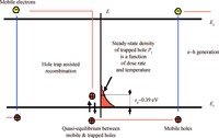
The tail of density of localized state in disordered oxides can also be interpreted as a set of shallow traps with the energy depths distributed over a range of a few tenths of eV above the SiO2 valence band edge (see, Figure 1). These hole localized states can under irradiation accumulate a lot of trapped holes, especially at low temperatures. As indicated in Reference [5], a bulk density of a localized hole at steady-state irradiation is proportional to a current value of dose rate, inversely proportional to the squared oxide electric field magnitude. It should also be proportional to the Arrhenius exponent exp ( εp /kT ), where εp is an average energy depth of the hole localized levels. This large exponent factor characterizes the ratio of the localized to the mobile hole densities at steady-state irradiation.
 DownLoad:
The occurrence of such steady-state positive bulk charge can manifest itself at least via two experimentally observable consequences. First, this bulk density of localized traps enhances recombination and it limits in such a way the effective charge yield. Reduction of the charge yield with a dose rate increase is known as the ELDRS effect. A finite number of the localized hole states implies that the electron-hole recombination rate and the charge yield (and ELDRS effect) have to be saturated for sufficiently high dose rates. We study this effect in Section 3.
Second, the “freezing”[13] of a large amount of radiation-induced holes under low-temperature irradiation can lead to temperature instabilities. In particular, as has been shown in Reference [14], the warm-up after low-temperature (< 125 K) irradiation leads to significant increase in degradation due to a release of localized holes at room temperatures followed by the hole transport to the interfaces. Similar behavior takes place in MOS oxides[13, 15].
The dispersive transport of radiation-induced holes proceeds through the combined tunnel and/or thermally activated hopping between the neighbor or, in some sense, optimal localized states, which can be described by the continuous time random walk model (CTRW)[16-18]. Due to a strong scatter of the hopping time constants, the hole transport in SiO2 has a dispersive, strongly delayed character, and it is very sensitive to temperature and electric field.
In previous work[19], it was briefly discussed that these experiments can be explained quantitatively within a framework of the modified model of the effective charge yield limited by delayed trap-assisted recombination, developed for the ELDRS effects description[5-7]. We intend to address these issues in more depth in this work.
2. Defect precursor density depletion as a possible saturation mechanism
A common cause of dose degradation in the CMOS and bipolar devices is the radiation defect buildup near or at the Si-SiO2 interface. The radiation-induced hole flux $\phi_{\rm p} $ through the interface can be described for an appropriate electric field polarity as follows
|
${{\phi }_{\text{p}}}={{\eta }_{\text{eff}}}\left( {{E}_{\text{ox}}} \right){{K}_{\text{g}}}P,{{d}_{\text{ox}}},$ |
(1) |
where P is a dose rate, ηeff (Eox is the effective charge yield[5], Eox is the oxide electric field magnitude, dox is the oxide thickness, Kg $\cong $ 8 × 1012 cm-3 rad (SiO2)-1 is the electron-hole pair generation rate constant in SiO2[20]. Near-interfacial defect buildup rate Gd [cm-2 s-1] is proportional to the hole flux $\phi_{\rm p}$, the deep hole capture cross-section ∑p(~ 10-15 cm-2[21]), and to the density of the unoccupied precursors (oxygen vacancies) for the deep hole traps on its effective thickness l
|
$Gd=∑p(NVO−pd)lϕp=Ftηeff(Eox)KgPdox−pd∑plηeff(Eox)KgPdox, $
|
(2) |
where pd is the radiation defect bulk density. This equation can be rewritten in a concise form
|
${{G}_{\text{d}}}={{F}_{\text{t}}}{{A}_{\text{d}}}P-\text{ }{{p}_{\text{d}}}l/{{\tau }_{\text{V}}}\text{ }$ |
(3) |
where Ad ηeff(Eox)Kgdox , Ft =∑pNVOl is a dimensionless constant having a meaning of the defect trapping efficiency in a linear region of dose curve, τV is the dose-rate-dependent time constant, defined as follows
|
$\tau _{\text{V}}^{-1}=\sum\nolimits_{\text{p}}{{{\eta }_{\text{eff}}}}\left( {{E}_{\text{ox}}} \right){{K}_{\text{g}}}{{d}_{\text{ox}}}P.$ |
(4) |
Sure, the defect density cannot be greater than the precursor bulk density NVO. Therefore, even if there is no annealing, the defect buildup rate would reduce under steady-state irradiation to almost zero value for the times t>τV .
A very important parameter of physical modeling is the defect surface concentration ΔNd =pdl . Despite extremely difficult and largely obscure character of buildup and transformation of recombination centers (interface traps) and the oxide charged traps, it is very reasonable and instructive to assume that the radiation-induced degradation is strongly correlated with ΔNd. The rate equation for ΔNd in the presence of thermal annealing takes the form
|
$\frac{\text{d}\Delta {{N}_{\text{d}}}}{\text{d}t}={{F}_{\text{t}}}{{A}_{\text{d}}},P-\Delta {{N}_{\text{d}}}\left( \frac{1}{{{\tau }_{\text{a}}}}+\frac{1}{{{\tau }_{\text{V}}}} \right).$ |
(5) |
Thermal annealing is a fundamental process, and it is inherent both to the devices of bipolar and CMOS technologies. However, the annealing parameters τa(T)=$\Delta {{N}_{\text{d}}}\left( D \right)={{F}_{\text{t}}}{{A}_{\text{d}}}\left( {{E}_{\text{ox}}} \right), P\tau _{\text{rd}}^{\text{eff}}\left[ 1-\exp \left( -\frac{D}{P\tau _{\text{rd}}^{\text{eff}}} \right) \right], $a0 exp (εa /kT) (εa is the annealing activation energy, and τa0 is the annealing time constant, T is temperature, k is the Boltzmann constant) can be specific to different technologies or, even, for different devices.
At relatively low doses (< 100 krad), when the constants in the rate equation can be considered as dose-independent, Equation. (5) for steady-state irradiation with a constant dose rate has a simple analytic solution
|
$\Delta {{N}_{\text{d}}}\left( D \right)={{F}_{\text{t}}}{{A}_{\text{d}}}\left( {{E}_{\text{ox}}} \right),P\tau _{\text{rd}}^{\text{eff}}\left[ 1-\exp \left( -\frac{D}{P\tau _{\text{rd}}^{\text{eff}}} \right) \right],$ |
(6) |
where the effective annealing time constant τrdeff =( {τa-1 +τV-1)-1 is defined. In fact, the effective annealing time constant is determined by the minimum of the time constants τrdeff $\cong $τa , τV . Particularly, when τa <τV or, equivalently, (∑p Ad)-1>Pτa , the thermal annealing process dominates and maximum degradation is determined by a dose-rate and temperature-dependent saturation value ΔNdSAT$\propto $Pτa .
|
$\Delta {{N}_{\text{d}}}\left( D \right)\cong {{F}_{\text{t}}}{{A}_{\text{d}}},P{{\tau }_{\text{a}}}\left[ 1-\exp \left( -\frac{D}{P{{\tau }_{\text{a}}}} \right) \right].$ |
(7) |
This case of thermal annealing corresponds to saturation dose which is proportional to dose rate and it is strongly temperature dependent due to the temperature dependence of the annealing time constant.
In contrast, if τV$\ll $τa , i.e. when the oxide is relatively thick, the dose rate is high enough and/or irradiation temperature is low enough, we have the saturation with a maximum degradation due to full precursor occupation
|
$\Delta {{N}_{\text{d}}}\left( D \right)\cong {{N}_{\text{VO}}}l\left[ 1-\exp \left( -{{\Sigma }_{\text{p}}}{{A}_{\text{d}}}D \right) \right].$ |
(8) |
The saturation dose does not depend in this case on dose rate explicitly but does implicitly via a dose rate dependence of the charge yield ηeff.
|
${{D}_{\text{SAT}}}={{\left( {{\eta }_{\text{eff}}}{{K}_{\text{g}}}{{\Sigma }_{\text{p}}}{{d}_{\text{ox}}} \right)}^{-1}}.$ |
(9) |
Temperature-independent value of saturated degradation is thus a hallmark of the precursor depletion saturation.
The demarcation line between these two saturation types, defined by an equation
|
${{\tau }_{\text{a}}}={{\left[ {{\eta }_{\text{eff}}}\left( {{E}_{\text{ox}}},T \right){{\Sigma }_{\text{p}}}{{K}_{\text{g}}}{{d}_{\text{ox}}}P \right]}^{-1}},$ |
(10) |
depends essentially on dose rate, temperature, electric field, and oxide thickness.
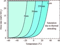
For example, the contour plot in Figure 2 shows the demarcation lines between the thermal annealing saturation and the precursor-depletion-induced saturation calculated for the different oxide thicknesses. Despite some uncertainties in parameters, it is clear that the precursor-depletion-induced saturation has to dominate in thick oxides, especially at low temperatures and relatively high dose rates. In particular, there is much experimental evidence that degradation in bipolar devices saturates at the dose rates 10 - 100 rad/s and at the time ~103 s[22] which is several orders of magnitude lower than the time constant of thermal annealing at room temperature.
Low dose rate space condition at a room temperature corresponds typically to a thermal annealing dominance while the relatively high dose rate ground tests can lead to the effects of the precursor trap depletion-limited degradation. Besides, the pulsed high-dose-rate irradiation can be expected at sufficiently high doses per pulse as a typical case of depletion-limited degradation in thick oxides.
3. Degradation mechanisms modeling
3.1 Influence of finite concentration of volume hole traps on charge yield
We intend to show in this section that a finite capacity of the hole traps can modify the expression for the charge yield. The general kinetic equation system for mobile (n) and localized (nt) electrons and, correspondingly, holes (p and pt) has been investigated in Reference [5]. It included an equation for trapping-detrapping processes for holes
|
$\frac{\text{d}{{p}_{t}}}{dt}={{C}_{\text{p}}},p,({{N}_{\text{tp}}}-{{p}_{\text{t}}})-{{\gamma }_{\text{p}}},{{p}_{\text{t}}},$ |
(11) |
where Ntp is the effective density of hole localized states (traps) per unit of volume, Cp is the effective capture rate of holes (cm3/s), γp is the hole emission rate constant (s-1). A small hole trap occupancy assumption pt$\ll $Ntp was used in Reference [5]. This allowed us to consider the oxide as an infinite reservoir for the hole trapping so that the quasi-steady-state density (i.e., when dpt/dt = 0) of trapped holes turned out to be proportional to dose rate over a whole range of dose rates. The analysis shows this may not be the case at low irradiation temperatures and low electric fields in thick oxides.
We have found in Reference [23] that a consistent consideration of a finite value of the hole trap density leads to the same general view for the effective charge yield function ηeff as in Reference [5]
|
${{\eta }_{\text{eff}}}\left( P,T,{{d}_{\text{ox}}},{{E}_{\text{ox}}} \right)={{\eta }_{\text{G}}}({{E}_{\text{ox}}})\frac{\left( 1+4f \right){{,}^{1/2}}-1}{2f},$ |
(12) |
where an asymptotic of the yield function ηG(Eox) at high electric fields is assumed to be temperature-independent and normally interpolated at relatively high Eox by a monotonically increasing function of local electric field Eox
|
${{\eta }_{\text{G}}}({{E}_{\text{ox}}})={{\eta }_{0}}+\frac{{{E}_{\text{ox}}}/{{E}_{0}}\text{ }}{1+{{E}_{\text{ox}}}/{{E}_{0}}}\left( 1-{{\eta }_{0}} \right),$ |
(13) |
where η0 and E0 are the fitting constants parameterizing a high-field region of experimental dependence. The only difference is a definition of the modified dimensionless function f:
|
$f(P,T,{{d}_{\text{ox}}},{{E}_{\text{ox}}},{{N}_{\text{tp}}})\cong \frac{q,{{N}_{\text{tp}}}{{d}_{\text{dox}}}}{6{{\varepsilon }_{\text{ox}}}{{\varepsilon }_{0}},{{E}_{\text{ox}}}}\frac{b,{{d}_{\text{ox}}}}{1+b,{{d}_{\text{ox}}}/2},$ |
(14) |
with a function b({T, Eox), which is defined for brevity as
|
$b(T,{{E}_{\text{ox}}})=\frac{{{\eta }_{\text{G}}}{{K}_{\text{g}}}P}{{{\mu }_{\text{p}}}{{E}_{\text{ox}}}{{N}_{\text{tp}}}}\exp \frac{{{\varepsilon }_{\text{p}}}}{kT},$ |
(15) |
where μp is the oxide hole mobility, εox ε0 ($\cong $ 3.5 × 10⁻¹² F/cm) is the SiO2 permittivity, εp ($\cong $ 0.39 eV) is the effective energy depth of the hole localized states in the oxide bulk.
Note that Ntp is assumed, in fact, to be infinite in original versions of our model[5-7]. This corresponds to the case of incomplete occupation of the localized states (pt $\ll$ Ntp, or bdox $\ll$1) with the dose-rate-dependent f and ηeff
|
$f(P,T,dox,Eox,Ntp)≅q,ddox6εoxε0,EoxηGKgPdoxμp,EoxexpεpkBT. $
|
(16) |
At sufficiently high dose rates and/or at low temperatures (bdox >1), the trapped hole concentration saturates at a maximum level pt $\cong$ Ntp due to full occupation of the hole localized states. The charge yield function turns out to be dose-rate-independent in this case. A line demarcating the regions of different dose-rate sensitivity types is approximately defined by a condition bdox =1, or
|
$\frac{{{\eta }_{\text{G}}}{{K}_{\text{g}}}P{{d}_{\text{ox}}}}{{{\mu }_{\text{p}}}{{E}_{\text{ox}}}{{N}_{\text{tp}}}}\exp \left( \frac{{{\varepsilon }_{\text{p}}}}{kT} \right)=1.$ |
(17) |
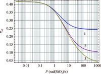
This equation is illustrated by a graph, shown in Figure 3.
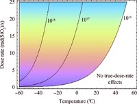
The impact of concentration Ntp on the effective charge yield dependence on dose rate is shown in Figure 4.

The range of noticeable dependence of the ηeff on dose rate is a window of the dose rate sensitivity. At extremely low dose rates an additional dose-rate-dependent recombination is negligible and the effective charge yield reaches its maximum dose-rate-independent value ηeff $\cong$ ηG ( Eox) (see Equation (13)). The right border of the dose-rate sensitivity window is determined by a capacity of the steady-state hole localized states (Ntp ) which restricts the maximum recombination electron-hole rate and, correspondingly, the minimum value of the charge yield. We found that a finite value of Ntp (~ 7 × 1017 cm3) provides the lower limit of the charge yield at low temperatures as high as 0.01-0.10, observed in the recent paper[10, 11].
3.2 Charge yield at low temperatures
Radiation response under low temperatures is often important in space applications. A reduced degradation of thick oxides was observed at low temperatures[9-11]. This effect can be explained by a decrease of the charge yield due to enhanced electron-hole recombination at low temperature. With the aim of the ELDRS effect explanation, starting in 2005, we have been developing an analytical model for the effective charge yield, limited by the delayed electron-hole trap-assisted recombination (see References [5-7]). According to this model, the charge yield efficiency has to decrease with temperature lowering due to enhanced recombination at low temperature.
Boesch and McLean[16] found that a portion of the radiation-induced holes can be stuck in the bulk of the thick oxides during the timescale as high as 103 s at room temperatures. We have figured out that the rate of the trap-assisted electron-hole recombination rate is proportional to the temperature-dependent quasi-steady-state density of such holes (
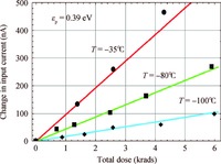
The proposed approach can explain the temperature-dependent character of the dose curves observed in the bipolar integrated circuits[10]. For simulation of dose degradation of input base current of the BJTs we use here a model proposed in Reference [24] (see Appendix).
The second term in the r.h.s. of (A2) can be ignored at low temperatures and/or at low doses. Then, the solution of (A2) at such conditions is a linear function of the dose. In this case, the slope of the dose curves at different temperatures is determined at a fixed collector current by the temperature dependence of the effective charge yield ηeff (see Equation (12)).

The points in Figure 5 (taken from Reference [10]) show experimental dependencies of the input bias current as the dose functions at different irradiation temperatures. Significantly less damage is observed for the samples irradiated at a lower temperature. The results of charge yield simulation at different temperatures exhibit excellent agreement with the experiment at an average depth of the hole trap states εp =0.39 eV. Remarkably, this value is coincident with the value determined experimentally in the original paper[5] from the slopes of the dose curves at room and slightly elevated temperatures.
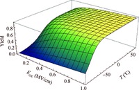
According to Equation (12), the temperature dependence is expected to be negligible at high electric fields and/or for thin oxides. For instance, Figure 6 illustrates the calculated dependence of the effective charge yield both on temperature and electric field.

Notice that ηeff is also a decreasing function of dose rate (ELDRS effect). This gives grounds to use irradiation at elevated temperatures for experimental imitation of the ELDRS effects.
4. Competition between the charge yield effects and thermal annealing
The true dose rate effect is determined by an explicit dependence of the charge yield on a current value of dose rate. Besides, the simultaneous thermal annealing during irradiation determines an implicit dependence of degradation on irradiation time, i.e. on the thermal and dose-rate pre-history.
Thus, there are the two types of the dose rate effects with the opposing responses to a dose rate change at a fixed dose. The former (typical for the bipolar technologies with relatively thick oxides) is associated with the explicitly decreasing dependence of εeff on dose rate (ELDRS). The latter (typical, for instance, for the thin gate oxides of the MOSFETs) is determined by the time-dependent simultaneous thermal annealing, which suppresses degradation due to an annealing time increase at low dose rates. Thus, a competition takes place between the oppositely directed true dose rate effect for the charge yield and the time-dependent thermal annealing effect.
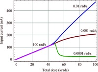
To illustrate this competition, we simulated with Equation (A2) the dose dependence of the input (base) current of a bipolar transistor with the dose rate switching. The simulated irradiation history was as follows. Initial degradation of the input current simulated with a dose rate 100 rad(SiO2)/s up to a dose 50 krad, followed by switching to 3 different dose rates (0.01, 0.001 and 0.0001 rad(SiO2)/s). Simulation results are shown in Figure 7. A dose rate switch to moderately low values causes an increase in degradation rate due to the ELDRS effect (increase in the charge yield). This is clearly seen from the upper curve in Figure 7.

At the same time, an increase in annealing time with lowering the dose rate at a fixed dose would lead to suppression of the ELDRS effects (intermediate curve in Figure 7), or, even up to appreciable annealing at ultra-low dose rates (the lower curve). Thus, a preliminary high dose irradiation may lead to different types of degradation behavior after switching to lower dose rates depending on a balance of the true dose rate (ELDRS) and the time-dependent annealing effects.
Another type of interplay between the time-dependent and the true-dose-rate effects can take place at irradiations with different temperatures. An increase in irradiation temperature, on the one hand, leads explicitly to a degradation rate enhancement via the charge yield factor εeff (true-dose-rate effect). On the other hand, the elevated irradiation temperatures manifest implicitly themselves as an increase in irradiation time and a corresponding enhanced annealing (time-dependent effect).
A competition between the two effects is illustrated in Figure 8. The dose curves were simulated for different irradiation temperatures and dose rates using the rate equation for the recombination current given in the Appendix[24, 25]. The precursor trap depletion effect was ignored at simulation, assuming thusτrdeff =τa0exp ( εa/kT. . Figure 8(a) shows the dose curves, simulated for different irradiation temperatures at a relatively high dose rate 10 rad/s. Total irradiation time is less in this case than a thermal annealing time constant τa even for a maximal irradiation temperature (50 ℃). Therefore, the annealing effects are minor in this case, and degradation increases with irradiation temperature through the dependence ηeff(T) as was the case in Figure 5[10].
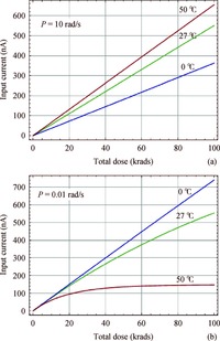
In contrast, an increase in an irradiation time at lower dose rates leads to the annealing enhancement, especially at higher temperatures. For instance, the degradation curve calculated for T=50 ℃ in Figure 8(b) turns out to be significantly suppressed and saturated due to thermal annealing at large irradiation times.
5. Summary and implications for hardness assurance
It was shown that the charge yield dependence on irradiation temperature and dose rate can be described in a unified manner. We find that a finite capacity of the hole density of states in the SiO2 bandgap (or, the same, the shallow hole trap concentration) can cause their full filling and related saturation in electron-hole recombination, accompanied by the suppression of the charge yield dose-rate sensitivity at high dose rates[23]. The complex interplay between the time-dependent and true-dose-rate effects is discussed and simulated in the context of proposed rate equation mathematical model.
A competition between the dose-rate and the time-dependent effects at different irradiation conditions (dose rate and temperature) can cause significant implications to the hardness assurance experiments. For instance, irradiation at elevated temperatures can lead to both an increase and a decrease in degradation depending on the other test conditions. Besides, low-dose-rate irradiation, to characterize the ELDRS effect, can be contaminated by simultaneous time-dependent thermal annealing effects depending on the dose rates, irradiation durations, and temperatures.
The importance of the precursor trap depletion processes was also shown, especially for irradiation response of the thick insulating oxides. These effects are absent in the low-dose-rate space environments with a thermal annealing dominance while the precursor trap depletion can be important at relatively high-dose-rate ground tests. A careful analysis of the test conditions and additional experiments may be needed to avoid misleading test results.
Appendix A: Rate equation for the recombination current
The input base current change is proportional to the recombination rate through the interfacial radiation-induced centers. The dose degradation of the base current and the radiation-induced gain change Δh21 are related by ΔIB =IC Δ(h21-1), where the collector current IC is typically observed to be dose-independent. The nature and detailed mechanisms of the interface recombination center creation and recombination current flow occurrence have still not been fully understood. Therefore, it is reasonable to assume that the recombination center buildup rate Frd , Ad P is proportional to an empirical “recombination center buildup efficiency” Frd which is assumed to be much less than 1. Assuming the neutral base surface recombination mechanism, the change in the base current ΔIB can be written as follows[24, 25]
|
$\Delta {{I}_{\text{B}}}={{I}_{\text{C}}}\frac{{{A}_{\text{S}}}}{{{A}_{\text{E}}}}\frac{{{\sigma }_{\text{r}}}{{v}_{\text{t}}}{{W}_{\text{B}}}}{{{D}_{\text{B}}}}\Delta {{N}_{\text{d}}},$ |
(A1) |
where AS (AE) is the area of the base - oxide interface (emitter-base junction), vt (~107 cm/s) is the carrier's thermal velocity, σr (~10-15 - 10-16 cm2) is the carrier's capture cross-section for the energy levels located near the Si midgap, WB is the base width, DB is the diffusivity of minority carriers in the base. Equation (A1) allows us to rewrite the rate Equation (5) as a rate equation for the excess input current ΔIB
|
$\frac{d\Delta {{I}_{\text{B}}}}{dt}={{F}_{\text{rd}}}\left( \frac{{{A}_{\text{S}}}}{{{A}_{\text{E}}}}\frac{{{\sigma }_{\text{r}}}{{v}_{\text{t}}}{{W}_{\text{B}}}}{{{D}_{\text{B}}}}{{I}_{\text{C}}} \right){{A}_{\text{d}}}\left( {{E}_{\text{ox}}} \right)P-\frac{\Delta {{I}_{\text{B}}}}{\tau _{\text{rd}}^{\text{eff}}}.$ |
(A2) |
A similar approach was validated in Reference [25].

 DownLoad: