J. Semicond. > 2022, Volume 43 > Issue 3 > 034102

ARTICLES

Performance enhancement of solution-processed InZnO thin-film transistors by Al doping and surface passivation

Wensi Cai, Haiyun Li, Mengchao Li and Zhigang Zang

+ Author Affiliations

 Corresponding author: Zhigang Zang, Email: zangzg@cqu.edu.cn

DOI: 10.1088/1674-4926/43/3/034102

PDF

Turn off MathJax

Abstract: 
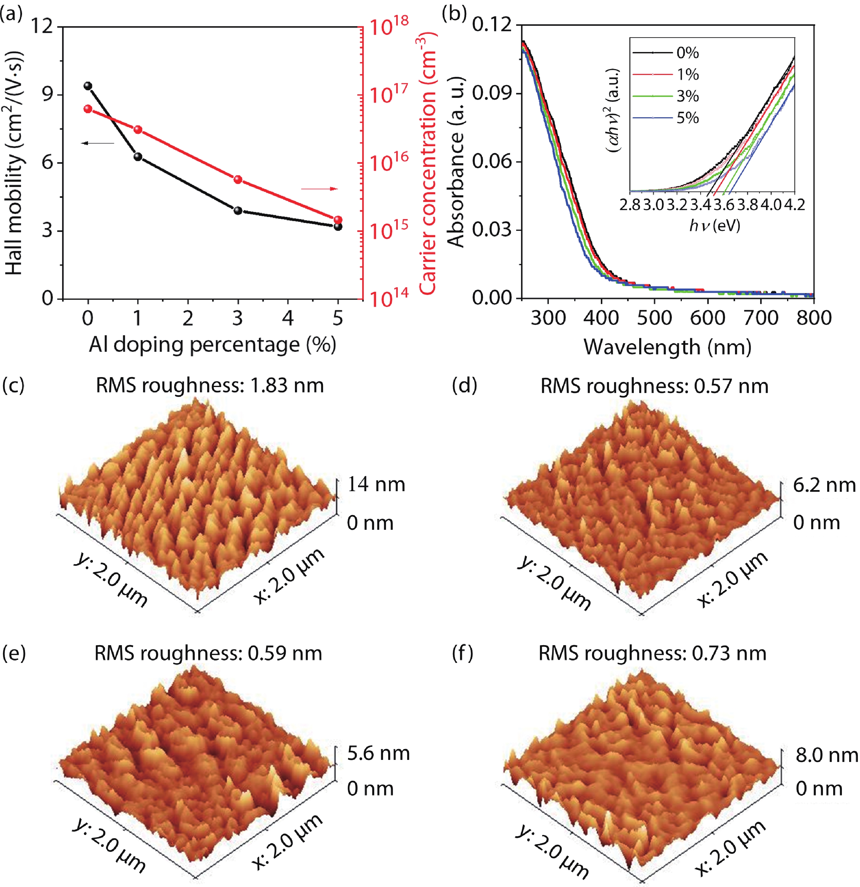
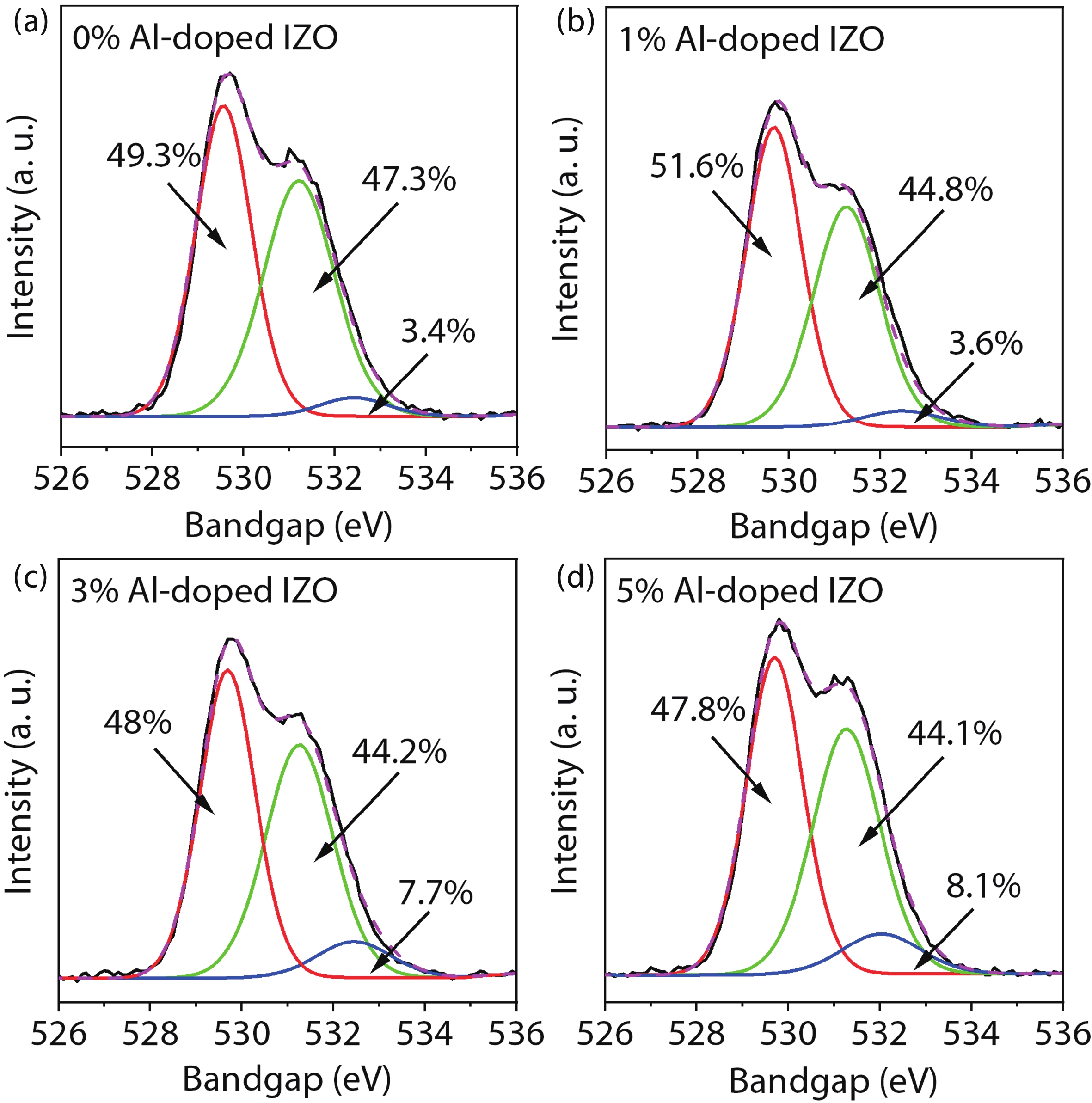
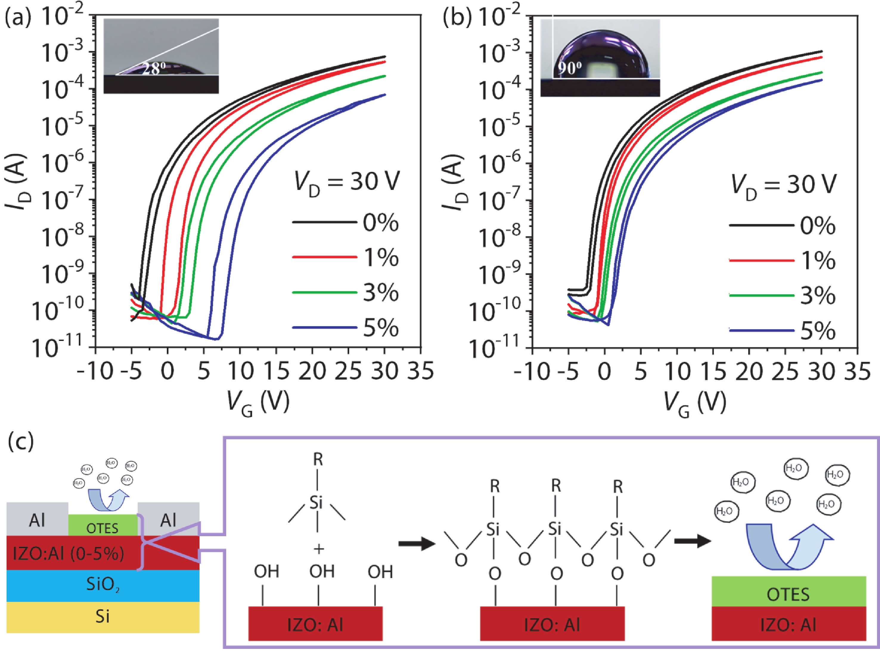
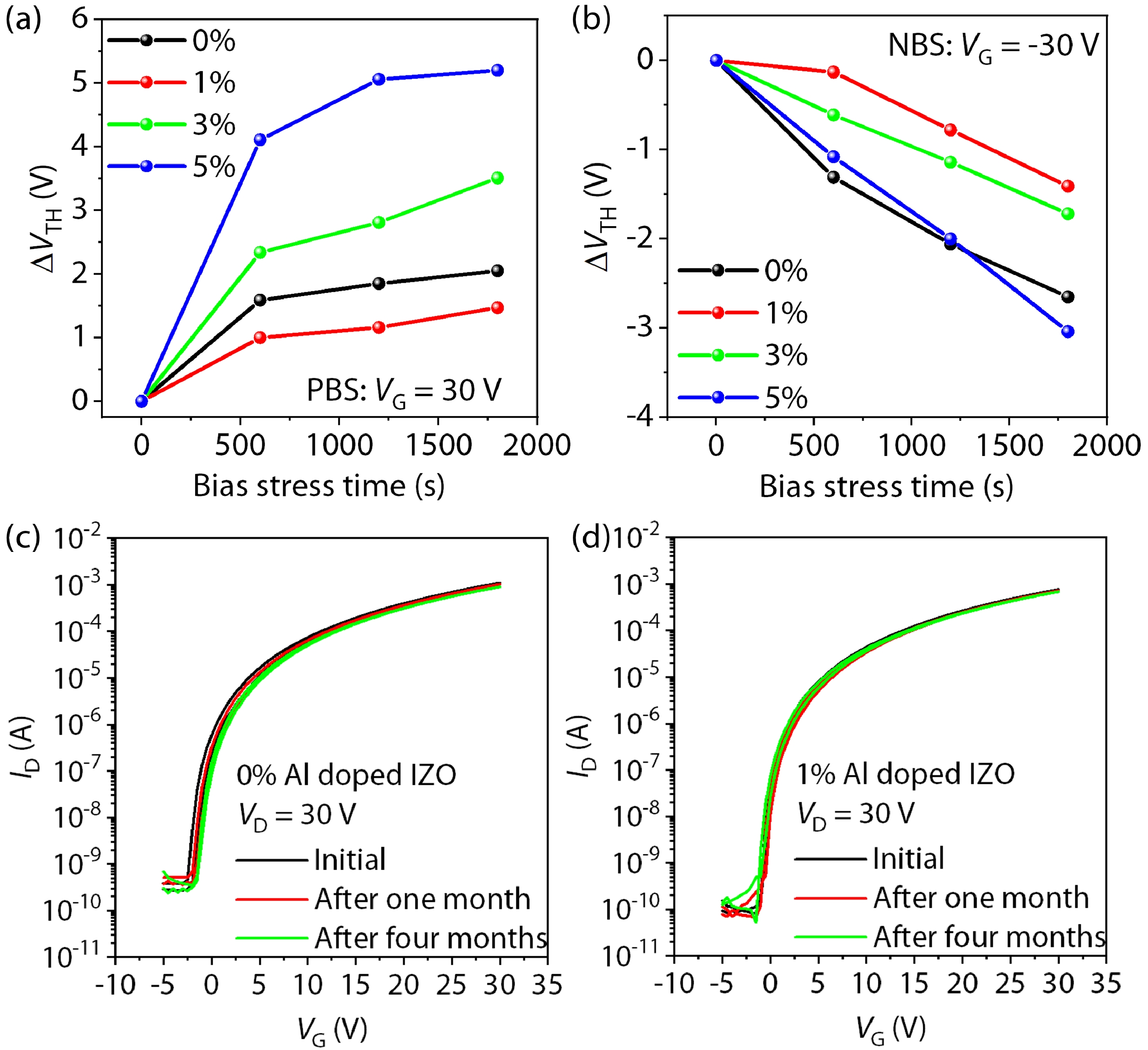
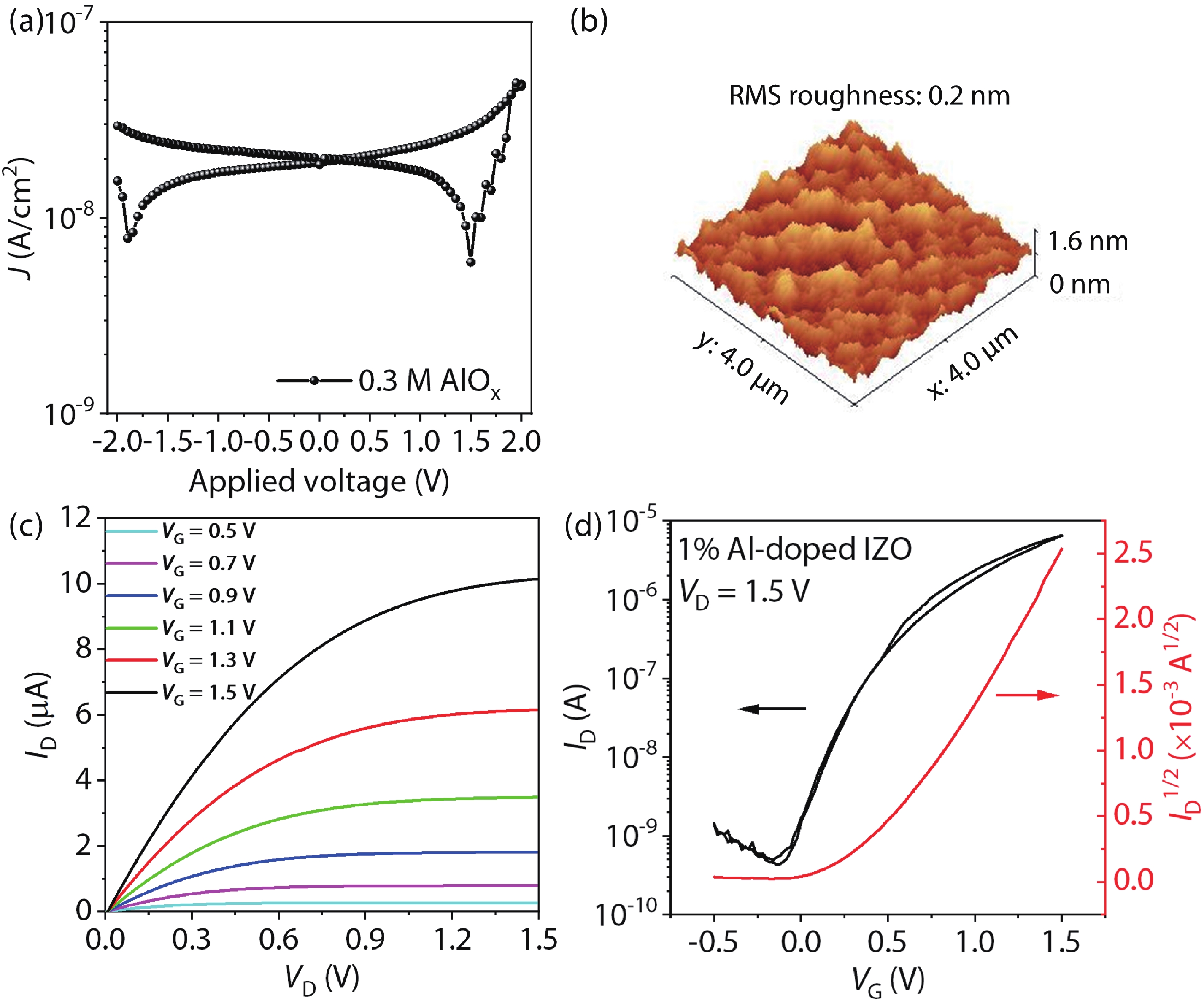
Solution-processed oxide semiconductors have been considered as a potential alternative to vacuum-based ones in printable electronics. However, despite spin-coated InZnO (IZO) thin-film transistors (TFTs) have shown a relatively high mobility, the lack of carrier suppressor and the high sensitivity to oxygen and water molecules in ambient air make them potentially suffer issues of poor stability. In this work, Al is used as the third cation doping element to study the effects on the electrical, optoelectronic, and physical properties of IZO TFTs. A hydrophobic self-assembled monolayer called octadecyltrimethoxysilane is introduced as the surface passivation layer, aiming to reduce the effects from air and understand the importance of top surface conditions in solution-processed, ultra-thin oxide TFTs. Owing to the reduced trap states within the film and at the top surface enabled by the doping and passivation, the optimized TFTs show an increased current on/off ratio, a reduced drain current hysteresis, and a significantly enhanced bias stress stability, compared with the untreated ones. By combining with high-capacitance AlOx, TFTs with a low operating voltage of 1.5 V, a current on/off ratio of > 104 and a mobility of 4.6 cm2/(V·s) are demonstrated, suggesting the promising features for future low-cost, low-power electronics.

Key words: thin-film transistorsoxide semiconductorsAl dopingsurface passivation


[1]
Nomura K, Ohta H, Takagi A, et al. Room-temperature fabrication of transparent flexible thin-film transistors using amorphous oxide semiconductors. Nature, 2004, 432, 488 doi: 10.1038/nature03090
[2]
Fortunato E, Barquinha P, Martins R. Oxide semiconductor thin-film transistors: a review of recent advances. Adv Mater, 2012, 24, 2945 doi: 10.1002/adma.201103228
[3]
Park J W, Kang B H, Kim H J. A review of low-temperature solution-processed metal oxide thin-film transistors for flexible electronics. Adv Funct Mater, 2020, 30, 1904632 doi: 10.1002/adfm.201904632
[4]
Cai W, Li H, Zang Z. One-volt, solution-processed InZnO thin-film transistors. IEEE Electron Device Lett, 2021, 42, 525 doi: 10.1109/LED.2021.3062422
[5]
Park W J, Shin H S, Ahn B D, et al. Investigation on doping dependency of solution-processed Ga-doped ZnO thin film transistor. Appl Phys Lett, 2008, 93, 083508 doi: 10.1063/1.2976309
[6]
Zhong D Y, Li J, Zhou Y H, et al. The material properties of novel boron doped InZnO thin films by solution process and its application in thin film transistors with enhanced thermal stability. Superlattices Microstruct, 2018, 122, 377 doi: 10.1016/j.spmi.2018.07.004
[7]
Jeon H J, Maeng W J, Park J S. Effect of Al concentration on the electrical characteristics of solution-processed Al doped ZnSnO thin film transistors. Ceram Int, 2014, 40, 8769 doi: 10.1016/j.ceramint.2014.01.098
[8]
Reed A, Stone C, Roh K, et al. The role of third cation doping on phase stability, carrier transport and carrier suppression in amorphous oxide semiconductors. J Mater Chem C, 2020, 8, 13798 doi: 10.1039/D0TC02655G
[9]
Cai W, Wilson J, Zhang J, et al. Significant performance enhancement of very thin InGaZnO thin-film transistors by a self-assembled monolayer treatment. ACS Appl Electron Mater, 2020, 2, 301 doi: 10.1021/acsaelm.9b00791
[10]
Cai W, Zang Z, Ding L. Self-assembled monolayers enhance the performance of oxide thin-film transisotrs. J Semicond, 2021, 42, 030203 doi: 10.1088/1674-4926/42/3/030203
[11]
Zhong W, Li G, Lan L, et al. InSnZnO thin-film transistors with vapor-phase self-assembled monolayer as passivation layer. IEEE Electron Device Lett, 2019, 39, 1680 doi: 10.1109/LED.2018.2872352
[12]
Nayak P K, Hedhili M N, Cha D, et al. Impact of soft annealing on the performance of solution-processed amorphous zinc tin oxide thin-film transistors. ACS Appl Mater Interfaces, 2013, 5, 3587 doi: 10.1021/am303235z
[13]
Kim Y G, Kim T, Avis C, et al. Stable and high-performance indium oxide thin-film transistor by Ga doping. IEEE Trans Electron Devices, 2016, 63, 1078 doi: 10.1109/TED.2016.2518703
[14]
Cai W, Wilson J, Song A. Present status of electric-double-layer thin-film transistors and their applications. Flex Print Electron, 2021, 6, 043001 doi: 10.1088/2058-8585/ac039f
[15]
Kim D N, Kim D L, Kim G H, et al. The effect of La in InZnO systems for solution-processed amorphous oxide thin-film transistors. Appl Phys Lett, 2010, 97, 192105 doi: 10.1063/1.3506503
[16]
Bukke R N, Saha J K, Mude N N, et al. Lanthanum doping in zinc oxide for highly reliable thin-film transistors on flexible substrates by spray pyrolysis. ACS Appl Mater Interfaces, 2020, 12, 35164 doi: 10.1021/acsami.0c05151
[17]
Choi J, Park J, Lim K H, et al. Photosensitivity of InZnO thin-film transistors using a solution process. Appl Phys Lett, 2016, 109, 132105 doi: 10.1063/1.4963881
[18]
Lee K H, Park J H, Yoo Y B, et al. Effects of solution temperature on solution-processed high-performance metal oxide thin-film transistors. ACS Appl Mater Interfaces, 2013, 5, 2585 doi: 10.1021/am3032629
[19]
Zhong D, Li J, Zhao C, et al. Enhanced electrical performance and negative bias illumination stability of solution-processed InZnO thin-film transistor by boron addition. IEEE Trans Electron Devices, 2018, 65, 520 doi: 10.1109/TED.2017.2779743
[20]
Li J, Huang C X, Fu Y Z, et al. Amorphous LaZnSnO thin films by a combustion solution process and application in thin film transistors. Electron Mater Lett, 2016, 12, 76 doi: 10.1007/s13391-015-5302-8
[21]
Yang C, Li Y, Li J. Ab initio total energy study of ZnO adsorption on a sapphire (0001) surface. Phys Rev B, 2004, 70, 045413 doi: 10.1103/PhysRevB.70.045413
[22]
Wang D, Jiang J, Furuta M. Investigation of carrier generation mechanismin fluorine-doped n+-In–Ga–Zn–O for self-aligned thin-film transistors. J Display Technol, 2016, 12, 258 doi: 10.1109/JDT.2015.2472981
[23]
Luo Y R. Comprehensive handbook of chemical bond energies. CRC Press, 2007
[24]
Xu W, Liu D, Wang H, et al. Facile passivation of solution-processed InZnO thin-film transistors by octadecylphosphonic acid self-assembled monolayers at room temperature. Appl Phys Lett, 2014, 104, 173504 doi: 10.1063/1.4874303
[25]
Shao L, Nomura K, Kamiya T, et al. Operation characteristics of thin-film transistors using very thin amorphous In–Ga–Zn–O channels. Electrochem Solid St Lett, 2011, 14, H197 doi: 10.1149/1.3555070
[26]
Lopes M E, Gomes H L, Medeiros M C R, et al. Gate-bias stress in amorphous oxide semiconductors thin-film transistors. Appl Phys Lett, 2009, 95, 063502 doi: 10.1063/1.3187532
[27]
Jeong J K, Won Yang H, Jeong J H, et al. Origin of threshold voltage instability in indium-gallium-zinc oxide thin film transistors. Appl Phys Lett, 2008, 93, 123508 doi: 10.1063/1.2990657
[28]
Jeong Y, Bae C, Kim D, et al. Bias-stress-stable solution-processed oxide thin film transistors. ACS Appl Mater Interfaces, 2010, 2, 611 doi: 10.1021/am900787k
[29]
Suresh A, Muth J F. Bias stress stability of indium gallium zinc oxide channel based transparent thin film transistors. Appl Phys Lett, 2008, 92, 033502 doi: 10.1063/1.2824758
[30]
Choi W S, Jo H, Kwon M S, et al. Control of electrical properties and gate bias stress stability in solution-processed a-IZO TFTs by Zr doping. Curr Appl Phys, 2014, 14, 1831 doi: 10.1016/j.cap.2014.10.018
[31]
Cai W, Park S, Zhang J, et al. One-volt IGZO thin-film transistors with ultra-thin, solution-processed Al xO y gate dielectric. IEEE Electron Device Lett, 2018, 39, 375 doi: 10.1109/LED.2018.2798061
[32]
Lan L, Peng J. High-performance indium–gallium–zinc oxide thin-film transistors based on anodic aluminum oxide. IEEE Trans Electron Devices, 2011, 58, 1452 doi: 10.1109/TED.2011.2115248
[33]
Mukherjee A, Ottapilakkal V, Sagar S, et al. Ultralow-voltage field-effect transistors using nanometer-thick transparent amorphous indium–gallium–zinc oxide films. ACS Appl Nano Mater, 2021, 4, 8050 doi: 10.1021/acsanm.1c01326
[34]
Ning H, Zhou S, Cai W, et al. Fabrication of high-performance solution processed thin film transistors by introducing a buffer layer. Appl Surf Sci, 2020, 504, 144360 doi: 10.1016/j.apsusc.2019.144360
[35]
Ko J, Kim J, Park S Y, et al. Solution-processed amorphous hafnium-lanthanum oxide gate insulator for oxide thin-film transistors. J Mater Chem C, 2014, 2, 1050 doi: 10.1039/C3TC31727G
[36]
Moreira M, Carlos E, Dias C, et al. Tailoring IGZO composition for enhanced fully solution-based thin film transistors. Nanomaterials, 2019, 9, 1273 doi: 10.3390/nano9091273
[37]
Xia W, Xia G, Tu G, et al. Sol-gel processed high-k aluminum oxide dielectric films for fully solution-processed low-voltage thin-film transistors. Ceram Int, 2018, 44, 9125 doi: 10.1016/j.ceramint.2018.02.120
[38]
Zhang Q, Ruan C, Xia G, et al. Low-temperature solution-processed InGaZnO thin film transistors by using lightwave-derived annealing. Thin Solid Films, 2021, 723, 138594 doi: 10.1016/j.tsf.2021.138594
[39]
Avis C, Kim Y G, Jang J. Solution processed hafnium oxide as a gate insulator for low-voltage oxide thin-film transistors. J Mater Chem, 2012, 22, 17415 doi: 10.1039/c2jm33054g
[40]
Jiang G, Liu A, Liu G, et al. Solution-processed high-k magnesium oxide dielectrics for low-voltage oxide thin-film transistors. Appl Phys Lett, 2016, 109, 183508 doi: 10.1063/1.4966897
Fig. 1.  (Color online) (a) Hall mobility and carrier concentration of the IZO:Al films. (b) Absorbance and corresponding bandgap (inset) of the IZO:Al films. Surface morphology of IZO films doped with (c) 0%, (d) 1%, (e) 3% and (f) 5% Al.

Fig. 2.  (Color online) O 1s spectra of IZO:Al films doped with (a) 0%, (b) 1%, (c) 3% and (d) 5% Al.

Fig. 3.  (Color online) Transfer characteristics of IZO:Al TFTs (a) without and (b) with an OTES top surface treatment. The insets show images of a water drop on the surface of the IZO:Al films. (c) Schematic diagrams of TFT structures and OTES formation on IZO:Al surface. R represents C18H37.

Fig. 4.  (Color online) Threshold voltage shift of IZO:Al TFTs under (a) a positive bias stress (PBS) and (b) a negative bias stress (NBS). Transfer characteristics of (c) 0% and (d) 1% Al doped IZO TFTs before and after being stored in ambient air for 4 months.

Fig. 5.  (Color online) (a) Current density as a function of applied voltage for Si/AlOx/Al capacitors. (b) Surface morphology of AlOx. (c) Output and (d) transfer characteristics of low-voltage IZO:Al TFTs.

Table 1.   Electrical properties of IZO:Al TFTs.

Al doping percentageTreatment or notCurrent on/off ratio (106)VTH (V)SS (V/dec)μ (cm2/(V·s))Dtotal (1012 cm–2 eV–1)
0%No3.85.670.723.92.38
Yes4.15.50.615.61.98
1%No86.60.643.52.09
Yes106.350.574.21.84
3%No4.810.20.691.782.27
Yes4.87.970.591.871.91
5%No3.912.720.690.812.27
Yes4.39.240.61.321.95
DownLoad: CSV

Table 2.   Electrical performance of low-voltage, solution-processed oxide TFTs.

μ
(cm2/(V·s))
VG range (V)VON (V)ION/IOFFVTH (V)SS
(V/dec)
Dtotal
(1012 cm–2eV–1)
Ref.
4.6–0.5 to 1.5–0.081.4 × 1040.50.171.6This work
0.06–0.5 to 1–0.3>1050.20.08512[33]
0.15–0.5 to 1–0.25~1040.0013//[35]
3.2–1 to 20.18106/0.073/[36]
7.23–1 to 303.06 × 1061.32//[37]
13.4–1 to 3–0.7>1050.44//[38]
1.05–5 to 50.21070.180.105/[39]
5.48–2 to 6/1070.720.339[40]
DownLoad: CSV
[1]
Nomura K, Ohta H, Takagi A, et al. Room-temperature fabrication of transparent flexible thin-film transistors using amorphous oxide semiconductors. Nature, 2004, 432, 488 doi: 10.1038/nature03090
[2]
Fortunato E, Barquinha P, Martins R. Oxide semiconductor thin-film transistors: a review of recent advances. Adv Mater, 2012, 24, 2945 doi: 10.1002/adma.201103228
[3]
Park J W, Kang B H, Kim H J. A review of low-temperature solution-processed metal oxide thin-film transistors for flexible electronics. Adv Funct Mater, 2020, 30, 1904632 doi: 10.1002/adfm.201904632
[4]
Cai W, Li H, Zang Z. One-volt, solution-processed InZnO thin-film transistors. IEEE Electron Device Lett, 2021, 42, 525 doi: 10.1109/LED.2021.3062422
[5]
Park W J, Shin H S, Ahn B D, et al. Investigation on doping dependency of solution-processed Ga-doped ZnO thin film transistor. Appl Phys Lett, 2008, 93, 083508 doi: 10.1063/1.2976309
[6]
Zhong D Y, Li J, Zhou Y H, et al. The material properties of novel boron doped InZnO thin films by solution process and its application in thin film transistors with enhanced thermal stability. Superlattices Microstruct, 2018, 122, 377 doi: 10.1016/j.spmi.2018.07.004
[7]
Jeon H J, Maeng W J, Park J S. Effect of Al concentration on the electrical characteristics of solution-processed Al doped ZnSnO thin film transistors. Ceram Int, 2014, 40, 8769 doi: 10.1016/j.ceramint.2014.01.098
[8]
Reed A, Stone C, Roh K, et al. The role of third cation doping on phase stability, carrier transport and carrier suppression in amorphous oxide semiconductors. J Mater Chem C, 2020, 8, 13798 doi: 10.1039/D0TC02655G
[9]
Cai W, Wilson J, Zhang J, et al. Significant performance enhancement of very thin InGaZnO thin-film transistors by a self-assembled monolayer treatment. ACS Appl Electron Mater, 2020, 2, 301 doi: 10.1021/acsaelm.9b00791
[10]
Cai W, Zang Z, Ding L. Self-assembled monolayers enhance the performance of oxide thin-film transisotrs. J Semicond, 2021, 42, 030203 doi: 10.1088/1674-4926/42/3/030203
[11]
Zhong W, Li G, Lan L, et al. InSnZnO thin-film transistors with vapor-phase self-assembled monolayer as passivation layer. IEEE Electron Device Lett, 2019, 39, 1680 doi: 10.1109/LED.2018.2872352
[12]
Nayak P K, Hedhili M N, Cha D, et al. Impact of soft annealing on the performance of solution-processed amorphous zinc tin oxide thin-film transistors. ACS Appl Mater Interfaces, 2013, 5, 3587 doi: 10.1021/am303235z
[13]
Kim Y G, Kim T, Avis C, et al. Stable and high-performance indium oxide thin-film transistor by Ga doping. IEEE Trans Electron Devices, 2016, 63, 1078 doi: 10.1109/TED.2016.2518703
[14]
Cai W, Wilson J, Song A. Present status of electric-double-layer thin-film transistors and their applications. Flex Print Electron, 2021, 6, 043001 doi: 10.1088/2058-8585/ac039f
[15]
Kim D N, Kim D L, Kim G H, et al. The effect of La in InZnO systems for solution-processed amorphous oxide thin-film transistors. Appl Phys Lett, 2010, 97, 192105 doi: 10.1063/1.3506503
[16]
Bukke R N, Saha J K, Mude N N, et al. Lanthanum doping in zinc oxide for highly reliable thin-film transistors on flexible substrates by spray pyrolysis. ACS Appl Mater Interfaces, 2020, 12, 35164 doi: 10.1021/acsami.0c05151
[17]
Choi J, Park J, Lim K H, et al. Photosensitivity of InZnO thin-film transistors using a solution process. Appl Phys Lett, 2016, 109, 132105 doi: 10.1063/1.4963881
[18]
Lee K H, Park J H, Yoo Y B, et al. Effects of solution temperature on solution-processed high-performance metal oxide thin-film transistors. ACS Appl Mater Interfaces, 2013, 5, 2585 doi: 10.1021/am3032629
[19]
Zhong D, Li J, Zhao C, et al. Enhanced electrical performance and negative bias illumination stability of solution-processed InZnO thin-film transistor by boron addition. IEEE Trans Electron Devices, 2018, 65, 520 doi: 10.1109/TED.2017.2779743
[20]
Li J, Huang C X, Fu Y Z, et al. Amorphous LaZnSnO thin films by a combustion solution process and application in thin film transistors. Electron Mater Lett, 2016, 12, 76 doi: 10.1007/s13391-015-5302-8
[21]
Yang C, Li Y, Li J. Ab initio total energy study of ZnO adsorption on a sapphire (0001) surface. Phys Rev B, 2004, 70, 045413 doi: 10.1103/PhysRevB.70.045413
[22]
Wang D, Jiang J, Furuta M. Investigation of carrier generation mechanismin fluorine-doped n+-In–Ga–Zn–O for self-aligned thin-film transistors. J Display Technol, 2016, 12, 258 doi: 10.1109/JDT.2015.2472981
[23]
Luo Y R. Comprehensive handbook of chemical bond energies. CRC Press, 2007
[24]
Xu W, Liu D, Wang H, et al. Facile passivation of solution-processed InZnO thin-film transistors by octadecylphosphonic acid self-assembled monolayers at room temperature. Appl Phys Lett, 2014, 104, 173504 doi: 10.1063/1.4874303
[25]
Shao L, Nomura K, Kamiya T, et al. Operation characteristics of thin-film transistors using very thin amorphous In–Ga–Zn–O channels. Electrochem Solid St Lett, 2011, 14, H197 doi: 10.1149/1.3555070
[26]
Lopes M E, Gomes H L, Medeiros M C R, et al. Gate-bias stress in amorphous oxide semiconductors thin-film transistors. Appl Phys Lett, 2009, 95, 063502 doi: 10.1063/1.3187532
[27]
Jeong J K, Won Yang H, Jeong J H, et al. Origin of threshold voltage instability in indium-gallium-zinc oxide thin film transistors. Appl Phys Lett, 2008, 93, 123508 doi: 10.1063/1.2990657
[28]
Jeong Y, Bae C, Kim D, et al. Bias-stress-stable solution-processed oxide thin film transistors. ACS Appl Mater Interfaces, 2010, 2, 611 doi: 10.1021/am900787k
[29]
Suresh A, Muth J F. Bias stress stability of indium gallium zinc oxide channel based transparent thin film transistors. Appl Phys Lett, 2008, 92, 033502 doi: 10.1063/1.2824758
[30]
Choi W S, Jo H, Kwon M S, et al. Control of electrical properties and gate bias stress stability in solution-processed a-IZO TFTs by Zr doping. Curr Appl Phys, 2014, 14, 1831 doi: 10.1016/j.cap.2014.10.018
[31]
Cai W, Park S, Zhang J, et al. One-volt IGZO thin-film transistors with ultra-thin, solution-processed Al xO y gate dielectric. IEEE Electron Device Lett, 2018, 39, 375 doi: 10.1109/LED.2018.2798061
[32]
Lan L, Peng J. High-performance indium–gallium–zinc oxide thin-film transistors based on anodic aluminum oxide. IEEE Trans Electron Devices, 2011, 58, 1452 doi: 10.1109/TED.2011.2115248
[33]
Mukherjee A, Ottapilakkal V, Sagar S, et al. Ultralow-voltage field-effect transistors using nanometer-thick transparent amorphous indium–gallium–zinc oxide films. ACS Appl Nano Mater, 2021, 4, 8050 doi: 10.1021/acsanm.1c01326
[34]
Ning H, Zhou S, Cai W, et al. Fabrication of high-performance solution processed thin film transistors by introducing a buffer layer. Appl Surf Sci, 2020, 504, 144360 doi: 10.1016/j.apsusc.2019.144360
[35]
Ko J, Kim J, Park S Y, et al. Solution-processed amorphous hafnium-lanthanum oxide gate insulator for oxide thin-film transistors. J Mater Chem C, 2014, 2, 1050 doi: 10.1039/C3TC31727G
[36]
Moreira M, Carlos E, Dias C, et al. Tailoring IGZO composition for enhanced fully solution-based thin film transistors. Nanomaterials, 2019, 9, 1273 doi: 10.3390/nano9091273
[37]
Xia W, Xia G, Tu G, et al. Sol-gel processed high-k aluminum oxide dielectric films for fully solution-processed low-voltage thin-film transistors. Ceram Int, 2018, 44, 9125 doi: 10.1016/j.ceramint.2018.02.120
[38]
Zhang Q, Ruan C, Xia G, et al. Low-temperature solution-processed InGaZnO thin film transistors by using lightwave-derived annealing. Thin Solid Films, 2021, 723, 138594 doi: 10.1016/j.tsf.2021.138594
[39]
Avis C, Kim Y G, Jang J. Solution processed hafnium oxide as a gate insulator for low-voltage oxide thin-film transistors. J Mater Chem, 2012, 22, 17415 doi: 10.1039/c2jm33054g
[40]
Jiang G, Liu A, Liu G, et al. Solution-processed high-k magnesium oxide dielectrics for low-voltage oxide thin-film transistors. Appl Phys Lett, 2016, 109, 183508 doi: 10.1063/1.4966897

21090015suppl.pdf

1

Heterojunction-engineered carrier transport in elevated-metal metal-oxide thin-film transistors

Xiao Li, Zhikang Ma, Jinxiong Li, Wengao Pan, Congwei Liao, et al.

Journal of Semiconductors, 2024, 45(10): 102301. doi: 10.1088/1674-4926/24040016

2

Indium–gallium–zinc–oxide thin-film transistors: Materials, devices, and applications

Ying Zhu, Yongli He, Shanshan Jiang, Li Zhu, Chunsheng Chen, et al.

Journal of Semiconductors, 2021, 42(3): 031101. doi: 10.1088/1674-4926/42/3/031101

3

Surface passivation of perovskite film for efficient solar cells

Yang (Michael) Yang

Journal of Semiconductors, 2019, 40(4): 040204. doi: 10.1088/1674-4926/40/4/040204

4

Giant spin injection into semiconductor and THz pulse emission

Zheng Feng

Journal of Semiconductors, 2019, 40(7): 070201. doi: 10.1088/1674-4926/40/7/070201

5

Oxide-based thin film transistors for flexible electronics

Yongli He, Xiangyu Wang, Ya Gao, Yahui Hou, Qing Wan, et al.

Journal of Semiconductors, 2018, 39(1): 011005. doi: 10.1088/1674-4926/39/1/011005

6

Boron-rich layer removal and surface passivation of boron-doped p–n silicon solar cells

Caixia Hou, Rui Jia, Ke Tao, Shuai Jiang, Pengfei Zhang, et al.

Journal of Semiconductors, 2018, 39(12): 122004. doi: 10.1088/1674-4926/39/12/122004

7

Review of recent progresses on flexible oxide semiconductor thin film transistors based on atomic layer deposition processes

Jiazhen Sheng, Ki-Lim Han, TaeHyun Hong, Wan-Ho Choi, Jin-Seong Park, et al.

Journal of Semiconductors, 2018, 39(1): 011008. doi: 10.1088/1674-4926/39/1/011008

8

Effects of interface trap density on the electrical performance of amorphous InSnZnO thin-film transistor

Yongye Liang, Kyungsoo Jang, S. Velumani, Cam Phu Thi Nguyen, Junsin Yi, et al.

Journal of Semiconductors, 2015, 36(2): 024007. doi: 10.1088/1674-4926/36/2/024007

9

First-principles calculations of Mg2X (X = Si, Ge, Sn) semiconductors with the calcium fluorite structure

Sandong Guo

Journal of Semiconductors, 2015, 36(5): 053002. doi: 10.1088/1674-4926/36/5/053002

10

Progress in complementary metal-oxide-semiconductor silicon photonics and optoelectronic integrated circuits

Hongda Chen, Zan Zhang, Beiju Huang, Luhong Mao, Zanyun Zhang, et al.

Journal of Semiconductors, 2015, 36(12): 121001. doi: 10.1088/1674-4926/36/12/121001

11

Chemical and electrical properties of (NH4)2S passivated GaSb surface

Dongyan Tao, Yu Cheng, Jingming Liu, Jie Su, Tong Liu, et al.

Journal of Semiconductors, 2015, 36(7): 073006. doi: 10.1088/1674-4926/36/7/073006

12

Large-signal characterizations of DDR IMPATT devices based on group Ⅲ-Ⅴ semiconductors at millimeter-wave and terahertz frequencies

Aritra Acharyya, Aliva Mallik, Debopriya Banerjee, Suman Ganguli, Arindam Das, et al.

Journal of Semiconductors, 2014, 35(8): 084003. doi: 10.1088/1674-4926/35/8/084003

13

Effective interface passivation of a Ge/HfO2 gate stack using ozone pre-gate treatment and ozone ambient annealing

Mei Zhao, Renrong Liang, Jing Wang, Jun Xu

Journal of Semiconductors, 2013, 34(6): 066005. doi: 10.1088/1674-4926/34/6/066005

14

A theoretical model of the femtosecond laser ablation of semiconductors considering inverse bremsstrahlung absorption

Lin Xiaohui, Zhang Chibin, Ren Weisong, Jiang Shuyun, Ouyang Quanhui, et al.

Journal of Semiconductors, 2012, 33(4): 046002. doi: 10.1088/1674-4926/33/4/046002

15

Fabrication of SiC nanowire thin-film transistors using dielectrophoresis

Dai Zhenqing, Zhang Liying, Chen Changxin, Qian Bingjian, Xu Dong, et al.

Journal of Semiconductors, 2012, 33(11): 114001. doi: 10.1088/1674-4926/33/11/114001

16

Comparison of electron transmittances and tunneling currents in an anisotropic TiNx/HfO2/SiO2/p-Si(100) metal–oxide–semiconductor (MOS) capacitor calculated using exponential- and Airy-wavefunction app

Fatimah A. Noor, Mikrajuddin Abdullah, Sukirno, Khairurrijal

Journal of Semiconductors, 2010, 31(12): 124002. doi: 10.1088/1674-4926/31/12/124002

17

A process simplification scheme for fabricating CMOS polycrystalline-Si thin film transistors

Juang Miin-Horng, Chang Chia-Wei, Shye Der-Chih, Hwang Chuan-Chou, Wang Jih-Liang, et al.

Journal of Semiconductors, 2010, 31(6): 064003. doi: 10.1088/1674-4926/31/6/064003

18

Sensitive properties of In-based compound semiconductor oxide to Cl2 gas

Zhao Wenjie, Shi Yunbo, Xiu Debin, Lei Tingping, Feng Qiaohua, et al.

Journal of Semiconductors, 2009, 30(3): 034010. doi: 10.1088/1674-4926/30/3/034010

19

Optical and electrical properties of N-doped ZnO and fabrication of thin-film transistors

Zhu Xiaming, Wu Huizhen, Wang Shuangjiang, Zhang Yingying, Cai Chunfeng, et al.

Journal of Semiconductors, 2009, 30(3): 033001. doi: 10.1088/1674-4926/30/3/033001

20

Equivalent Circuit Analysis of an RF Integrated Inductor with Ferrite Thin-Film

Ren Tianling, Yang Chen, Liu Feng, Liu Litian, Wang A Z, et al.

Chinese Journal of Semiconductors , 2006, 27(3): 511-515.

1. Kim, D., Yoo, K.S., Lee, C.-H. et al. High-throughput and performance InZnAlO thin film transistor on polyimide substrate via atmospheric pressure spatial atomic layer deposition. Journal of Alloys and Compounds, 2025. doi:10.1016/j.jallcom.2025.180031
2. Chen, L., Han, B., Sun, B. et al. Effect of Pr concentration and native defects on the structural, electronic and optical properties of Pr doped IZO by first-principles study. Materials Today Communications, 2025. doi:10.1016/j.mtcomm.2024.111155
3. Gui, Z., Zou, K., Xu, M. et al. High Mobility and Excellent Stability of Solution-Processed Heterojunction-Channel IGO/AIGO TFT. ACS Applied Electronic Materials, 2025. doi:10.1021/acsaelm.5c00072
4. Wang, Z., Chen, L., Wu, B. et al. The microstructural evolution and densification process of titanium or tin doped indium zinc oxide ceramic targets. Materials Science and Technology (United Kingdom), 2024, 40(14): 1023-1032. doi:10.1177/02670836241236922
5. Lephe, S., Raj, S.M.G.F., Janaki, S. et al. Optimization of structural, electrical, and magnetic properties of the solution-processed IZO MOSFET adopting spin coating technique and its performance. Journal of Materials Science: Materials in Electronics, 2024, 35(23): 1569. doi:10.1007/s10854-024-13331-8
6. Wu, B., Han, B., Sun, B. et al. Microstructural evolution during densification process of neodymium-doped indium zinc oxide ceramic targets and application for high mobility films. Ceramics International, 2024, 50(13): 24139-24147. doi:10.1016/j.ceramint.2024.04.145
7. Raja, T., Sekhar, K. Performance evaluation of GPVs in existing TFET and proposed DG-JL-TFET: enhancing the RF performance through qualitative and quantitative approaches. Applied Physics A: Materials Science and Processing, 2024, 130(6): 373. doi:10.1007/s00339-024-07526-3
8. Meriga, S., Bhowmick, B. Robustness of Raised Buried Oxide Ferro Electric Tunnel FET in presence of Temperature and Traps and its Analog/RF Performance. Applied Physics A: Materials Science and Processing, 2024, 130(4): 223. doi:10.1007/s00339-024-07357-2
9. Choi, A.R., Lim, D.H., Shin, S.-Y. et al. Review of Material Properties of Oxide Semiconductor Thin Films Grown by Atomic Layer Deposition for Next-Generation 3D Dynamic Random-Access Memory Devices. Chemistry of Materials, 2024, 36(5): 2194-2219. doi:10.1021/acs.chemmater.3c02223
10. Zheng, Y., Wu, Z., Tong, H. et al. Effects of La Doping on Persistent Photoconductivity of Solution-Processed InZnO Thin-Film Transistors. IEEE Transactions on Electron Devices, 2024, 71(10): 6061-6066. doi:10.1109/TED.2024.3446747
11. Zhang, X., Xu, L., Liang, R. et al. Effect of Indium Doping on Bias Stability in Dual-Target Co-Sputtering InZnSnO Thin-Film Transistors. IEEE Transactions on Electron Devices, 2023, 70(12): 6375-6380. doi:10.1109/TED.2023.3326115
12. Chen, F., Zhang, M., Wan, Y. et al. Advances in mobility enhancement of ITZO thin-film transistors: a review. Journal of Semiconductors, 2023, 44(9): 091602. doi:10.1088/1674-4926/44/9/091602
13. Cai, W., Li, M., Lu, S. et al. Heterojunction Channel Engineering in Performance Enhancement of Solution-Processed Oxide Thin-Film Transistors. IEEE Transactions on Electron Devices, 2023, 70(6): 3085-3091. doi:10.1109/TED.2023.3263816
14. Lee, T., Kim, K., Kim, H.-I. et al. Improved Negative Bias Stability of Sol-Gel-Processed SnO2Thin-Film Transistors with Vertically Controlled Carrier Concentrations. ACS Applied Electronic Materials, 2023, 5(5): 2670-2677. doi:10.1021/acsaelm.3c00147
15. Meriga, S., Bhowmick, B. Investigation of a dual gate pocket-doped drain engineered tunnel FET and its reliability issues. Applied Physics A: Materials Science and Processing, 2023, 129(2): 104. doi:10.1007/s00339-023-06394-7
16. Patil, A.R., Dongale, T.D., Kamat, R.K. et al. Spray deposited zinc tungstate thin film for non-volatile memory application. Materials Letters, 2022. doi:10.1016/j.matlet.2022.132494
17. Cai, W., Li, M., Li, H. et al. Significant performance and stability improvement of low-voltage InZnO thin-film transistors by slight la doping. Applied Physics Letters, 2022, 121(6): 062108. doi:10.1063/5.0100407
18. Lee, D., Lee, A., Kim, H.-D. IZO/ITO Double-Layered Transparent Conductive Oxide for Silicon Heterojunction Solar Cells. IEEE Access, 2022. doi:10.1109/ACCESS.2022.3192646
  • Search

    Advanced Search >>

    GET CITATION

    Wensi Cai, Haiyun Li, Mengchao Li, Zhigang Zang. Performance enhancement of solution-processed InZnO thin-film transistors by Al doping and surface passivation[J]. Journal of Semiconductors, 2022, 43(3): 034102. doi: 10.1088/1674-4926/43/3/034102
    W S Cai, H Y Li, M C Li, Z G Zang. Performance enhancement of solution-processed InZnO thin-film transistors by Al doping and surface passivation[J]. J. Semicond, 2022, 43(3): 034102. doi: 10.1088/1674-4926/43/3/034102
    shu

    Export: BibTex EndNote

    Article Metrics

    Article views: 2034 Times PDF downloads: 79 Times Cited by: 18 Times

    History

    Received: 17 December 2021 Revised: 03 November 2021 Online: Accepted Manuscript: 23 December 2021Uncorrected proof: 24 December 2021Published: 10 March 2022

    Catalog

      Email This Article

      User name:
      Email:*请输入正确邮箱
      Code:*验证码错误
      Wensi Cai, Haiyun Li, Mengchao Li, Zhigang Zang. Performance enhancement of solution-processed InZnO thin-film transistors by Al doping and surface passivation[J]. Journal of Semiconductors, 2022, 43(3): 034102. doi: 10.1088/1674-4926/43/3/034102 ****W S Cai, H Y Li, M C Li, Z G Zang. Performance enhancement of solution-processed InZnO thin-film transistors by Al doping and surface passivation[J]. J. Semicond, 2022, 43(3): 034102. doi: 10.1088/1674-4926/43/3/034102
      Citation:
      Wensi Cai, Haiyun Li, Mengchao Li, Zhigang Zang. Performance enhancement of solution-processed InZnO thin-film transistors by Al doping and surface passivation[J]. Journal of Semiconductors, 2022, 43(3): 034102. doi: 10.1088/1674-4926/43/3/034102 ****
      W S Cai, H Y Li, M C Li, Z G Zang. Performance enhancement of solution-processed InZnO thin-film transistors by Al doping and surface passivation[J]. J. Semicond, 2022, 43(3): 034102. doi: 10.1088/1674-4926/43/3/034102

      Performance enhancement of solution-processed InZnO thin-film transistors by Al doping and surface passivation

      DOI: 10.1088/1674-4926/43/3/034102
      More Information
      • Wensi Cai:received her PhD degree from University of Manchester in 2019. She joined Chongqing University as a postdoc researcher since 2020. Her research interests mainly focus on oxide semiconductor- and perovskite-based electron devices
      • Zhigang Zang:received his PhD degree from Kyushu University in 2011. He joined the School of Optoelectronic Engineering, Chongqing University, as a professor since 2014. His research interests mainly focus on the synthesis of II–VI, III–V semiconductor materials and their applications in solarcells, photodetectors and light emitting diodes
      • Corresponding author: Email: zangzg@cqu.edu.cn
      • Received Date: 2021-12-17
      • Revised Date: 2021-11-03
      • Available Online: 2023-11-22

      Catalog

        /

        DownLoad:  Full-Size Img  PowerPoint
        Return
        Return