1. Introduction
In 2000, Subramanian et al.[1] and Ramirez et al.[2] noticed that the dielectric permittivity (ε´) of a microcrystalline sample of perovskite derivative calcium-copper-titanate (CaCu3Ti4O12) abruptly jumps by a factor of 100 when heated above T = 90 K (at 1 kHz frequency). This material at T = 100 K exhibits a huge value of ε´ of the order of 104 and ε´ becomes weakly dependent on temperature for T = 100–320 K. These unusual and fascinating properties make them suitable for potent applications, such as in multilayer ceramic capacitors, devices for memory and high-density energy storage[3]. In 2003, Kretly et al.[4] successfully used CaCu3Ti4O12 substrates for microwave devices and antennas. In 2004, Chung et al.[5] observed highly non-ohmic current–voltage characteristics in CaCu3Ti4O12 with nonlinear coefficient ≈ 912. This leads to the use of this material as an efficient switching (varistor-type device) and gas sensing device. In 2012, Felix et al.[6] investigated thin films of CaCu3Ti4O12 for potential applications, such as gas sensing, rectification, and resistive switching. In 2016, it was demonstrated that this material could serve as photocatalytic and photoelectrochemical materials with an excellent performance in visible light[7]. Since then, pure and substituted CaCu3Ti4O12 and related materials in monocrystalline, microcrystalline, nanophasic, nanocomposites, and thin-film forms have been extensively researched for potential use in a wide range of applications. In 2020, Chhetry et al.[8] revealed a novel possibility for the easy design and development of superior CaCu3Ti4O12 based capacitive sensors with versatile characteristics. Chattopadhyay et al.[9] suggested the possible use of CaCu3Ti4O12 nanopowder for application in a humidity sensor. Many research reports describing the fundamentals of experimental and theoretical researches on CaCu3Ti4O12 based ceramic materials are available in the literature.
Varistors are voltage-dependent resistors that demonstrate strong nonlinear current versus voltage (I–V) characteristics. The electrical properties of varistors are chiefly influenced by grain-boundary interface states. The principal function of a varistor is to sense and control transient voltage surges. When a varistor is subjected to a high applied voltage, its impedance changes from a near open circuit to a highly conducting state, which results in the clamping of the transient voltage to a safe level and thus electronic components of high-cost electronic devices may be protected. Between 2016 and 2021, a limited number of research reports were published on J–E characteristics of CaCu3Ti4O12 cubic perovskites substituted with different metallic cation/cations. For example, the nonlinear electrical properties with high-performance dielectric behavior of CaCu2.95Cr0.05Ti4.1O12 have been studied by Prompa et al.[10]. The improvement of the breakdown field and the dielectric properties of Bi3+-Al3+ co-doped CaCu3Ti4O12 have been investigated by Ren et al.[11]. The dielectric properties, nonlinear electrical response, and microstructural evolution of CaCu3Ti4–xSnxO12 ceramics prepared by a double ball-milling process have been investigated by Boonlakhorn et al.[12]. Cortes et al.[13] performed dielectric and non-ohmic properties of Ca2Cu2Ti4–xSnxO12 multiphasic ceramic composites. Comparative studies on pure and Sr2+ and Ni2+ doped and co-doped ceramics with special emphasis on the enhancement of dielectric properties have been published by Rhouma et al.[14]. Wu et al.[15] accomplished the effect of Ba2+ substitution on microstructure and electrical properties of Ca1–xBaxCu3Ti4O12 ceramics. Enhanced nonlinear I–V response of Te4+ substituted CaCu3Ti4O12 ceramics has been studied by Barman et al.[16]. Meanwhile, the improvement in varistor properties of aliovalent Cr3+ substitution for Ti4+ in CaCu3Ti4–xCrxO12–δ series has been investigated by Grezebielucka et al.[17]. Sun et al. studied improved dielectric properties of In3+ and Ta4+ co-substituted CaCu3Ti4O12 ceramics prepared by spark plasma sintering[18]. Very high-performance dielectric and non-ohmic properties of X and R-type Ca1–1.5xHoxCu3Ti4O12/TiO2 ceramics have been investigated by Sriakdee et al.[19]. Finally, enhanced giant dielectric properties and improved electrical response in acceptor–donner (Al and Ta)-substituted CaCu3Ti4O12 polycrystalline ceramics have been carried out by Boonlakhorn et al.[20]. Unfortunately, these studies carry very limited and similar information, and were performed at T = 300 K. The same is the case with the thermal variation of dc electrical resistivity, ρdc (T), study. To the best of our knowledge, only a handful of research articles describing ρdc (T) characteristics of bulk[21-24] and thin films[25] of CaCu3Ti4O12 are available in the literature. This gap has motivated us to carry out a systematic study of current density versus electric field characteristics over a wide temperature range and thermal variation of dc resistivity study of polycrystalline samples of quadruple perovskite series, CaCu3–xTi4–xFe2xO12 with x = 0.0, 0.1, 0.3, 0.5, and 0.7.
Based on the following facts, the work presented in this communication is important as well as different from the existing literature. The electrical properties, J–E characteristics and dc resistivity of CaCu3–xTi4–xFe2xO12 with x = 0.0, 0.1, 0.3, 0.5, and 0.7 have been studied over a wide temperature range of T = 313 to 773 K as a function of Fe-concentration (x). The compositional variation of various electrical parameters (e.g., maximum current density, breakdown electric field, the temperature at which switching action takes place, Schottky barrier height, non-linearity coefficient, and activation energy) are determined and correlated with structural parameters (i.e., lattice constant, cationic distribution), microstructural parameters (i.e., grain size, microstrain, dislocation density) and positron annihilation lifetime (PAL) parameters (i.e., defect-specific positron lifetime, the concentration of vacancy defect). We have thoroughly investigated various physical properties of pristine and Fe3+-substituted CaCu3Ti4O12 ceramics, CaCu3–xTi4–xFe2xO12 with x = 0.0–0.7, in recent years (2018–2021)[26-37]. In the system, divalent, weak magnetic (1 Bohr magneton), Jahn-Teller Cu2+ ions, and tetravalent, non-magnetic Ti4+ ions are simultaneously replaced by highly magnetic (5 Bohr magneton), trivalent Fe3+ ions in the series of quadruple perovskites, CaCu3–xTi4–xFe2xO12 where x varies from 0.0 to 0.7. Thus, interesting improvements in electrical behavior are expected. This work blends fundamental and applied research.
2. Experimental details
A series of cubic perovskites, CaCu3–xTi4–xFe2xO12 with x = 0.0, 0.1, 0.3, 0.5 and 0.7, was prepared by the mixed oxide route. The complete details regarding the synthesis, crystallographic phase identification, and structural parameters including cationic distribution determination by employing Rietveld refinement of X-ray powder diffraction data and average grain size (D) estimation by analyzing scanning electron micrographs are given elsewhere[27, 33]. The measurements of current (I) versus applied signal voltage (V) (V = 0–400 V) (I–V characteristics) were carried out with the help of an Aplab made high-voltage dc regulated power supply (model no.׃ 7332) at temperatures ranging from T = 300–673 K using the two probe pressure contact method and a horizontal electric furnace. The cylindrically pelletized samples were rubbed with fine glass paper to give mirror-polished surfaces, and then cleaned with dilute hydrochloric acid and dimethyl ketone. To have perfect ohmic contact, microcracks on the surfaces were filled with a rubbing of graphite, and finally Al- foil was also kept on the surface. Instead of I–V characteristics, the traces of J versus E are taken into consideration, which eases the comparison between the I–V characteristics of the samples with varying thickness and surface area. A bi-terminal pressure contact method was employed to carry out the dc electrical resistivity measurement. The same set of the ceramic pellets, sample holder, vertical electric furnace, temperature indicator with thermocouple, and temperature controller used for thermal variation of I versus V characteristics was used to carry out temperature-dependent dc resistivity measurement. The resistance was directly measured using a mega-ohm meter supplied by BPL India. The thermal variation of resistance was obtained by keeping a sample holder containing a cylindrically pelletized sample in a horizontal electric furnace. For I–V characteristics and dc resistivity measurements as a function of temperature, an indigenously designed and fabricated sample holder was used. The holder consists of two ceramic beads with supporting metal roads. The spring-loaded brass electrode is introduced into the ceramic beads and pressed hard against the surface of the pellet. The second brass electrode is fixed at the other end. GELCO electronics private limited, India made PTS-7201 temperature indicator attached with K-type chromal-alumel thermocouple were used to measure the temperature of the pellet. The temperature of the furnace was controlled by maintaining the current passing through the heater employing a current controller (Bharat electrical Mumbai, India, made single phase auto-transformer). The resistance was noted during the cooling cycle at an interval of 20 °C in the temperature range of 300–773 K. A single set of temperature-dependent I–V characteristics and dc resistivity measurements have been performed.
3. Results and discussion
A careful structural analysis demonstrates that the x = 0.0–0.5 compositions are formed in the single phase with cubic perovskite crystal symmetry in the space group Im3. For the composition with x = 0.7, the aciculate but low intensity (~ 4.0 %) peak centered at 2θ = 25.6° is due to a trivial amount of anatase structure of well-crystallized TiO2[33]. The secondary phase is randomly distributed within the primary CaCu3Ti4O12 matrix. Thus, Fe3+ substitution is restricted to x = 0.7 in the present study. In Tables 1 and 2, the structural and microstructural parameters are compiled to illustrate the compositional and temperature-dependent J–E characteristics.
| Fe3+_ content (x) | Strain 10–4 | a (Å) ±0.002 Å | dx (g/cm3) | d (g/cm3) | f | D (μm) | δ (1010 m–2) | TsL (K) | Es (V/cm) T = 473 K | Jmax (mA/cm2) | Ea1 (eV) | Ea2 (eV) |
| 0.0 | –4.54 | 7.391 | 5.056 | 4.744 | 0.062 | 3.7 | 7.30 | 473 | 978 | 327 | 0.33 | 0.43 |
| 0.1 | –6.16 | 7.388 | 5.061 | 4.712 | 0.069 | – | – | 373 | 570 | 270 | 0.29 | 0.29 |
| 0.3 | –6.77 | 7.387 | 5.064 | 4.704 | 0.071 | 7.5 | 1.78 | 373 | 525 | 225 | 0.22 | 0.21 |
| 0.5 | –5.96 | 7.400 | 5.038 | 4.556 | 0.096 | 7.9 | 1.60 | 373 | 261 | 225 | 0.25 | 0.15 |
| 0.7 | –6.95 | 7.411 | 5.016 | 4.566 | 0.090 | 3.4 | 8.65 | 373 | 300 | 225 | 0.27 | 0.21 |
| TsL is the lowest temperature at which switching action takes place. Es is the threshold value of the electric field beyond which non-ohmic behavior is observed. Jmax is the maximum current density value. Ea1 and Ea2 are the activation energies determined from Arrhenius plots below and above the transition temperature, respectively. | ||||||||||||
 DownLoad:
CSV
| Show Table
DownLoad:
CSV
| Show Table
| Fe3+ content (x) | Cation distribution |
| 0.0 | Ca2+[Cu2+3] {Ti4+4}O2−12 |
| 0.1 | Ca2+[Cu2+2.86Fe3+0.14] {Ti4+3.90Fe3+0.06Cu2+0.04}O2−12 |
| 0.3 | Ca2+[Cu2+2.41Ti4+0.24Fe3+0.35] {Ti4+3.46Fe3+0.25Cu2+0.29}O2−12 |
| 0.5 | Ca2+[Cu2+2.03Ti4+0.17Fe3+0.80] {Ti4+3.33Fe3+0.20Cu2+0.47}O2−12 |
| 0.7 | Ca2+[Cu2+1.53Ti4+0.12Fe3+1.35] {Ti4+3.18Fe3+0.05Cu2+0.77}O2−12 |
DownLoad:
CSV
| Show Table
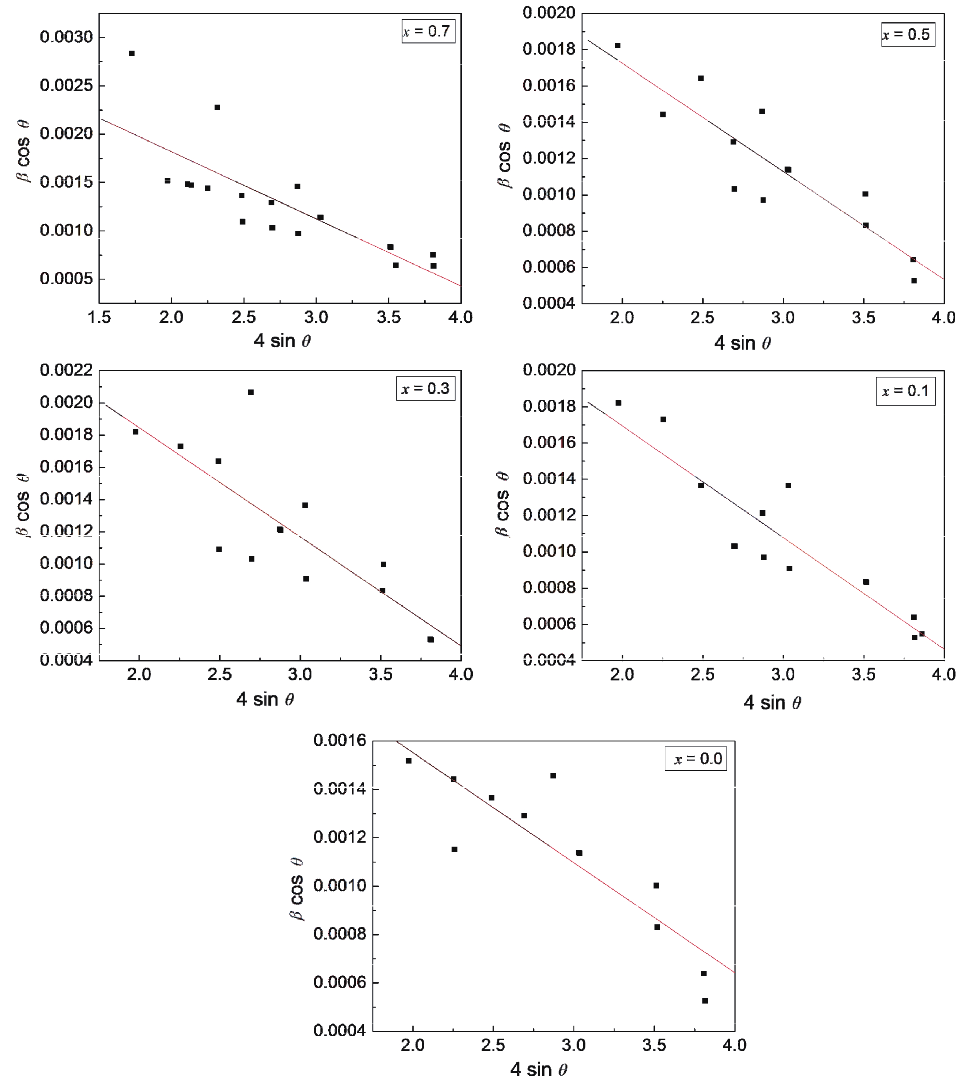
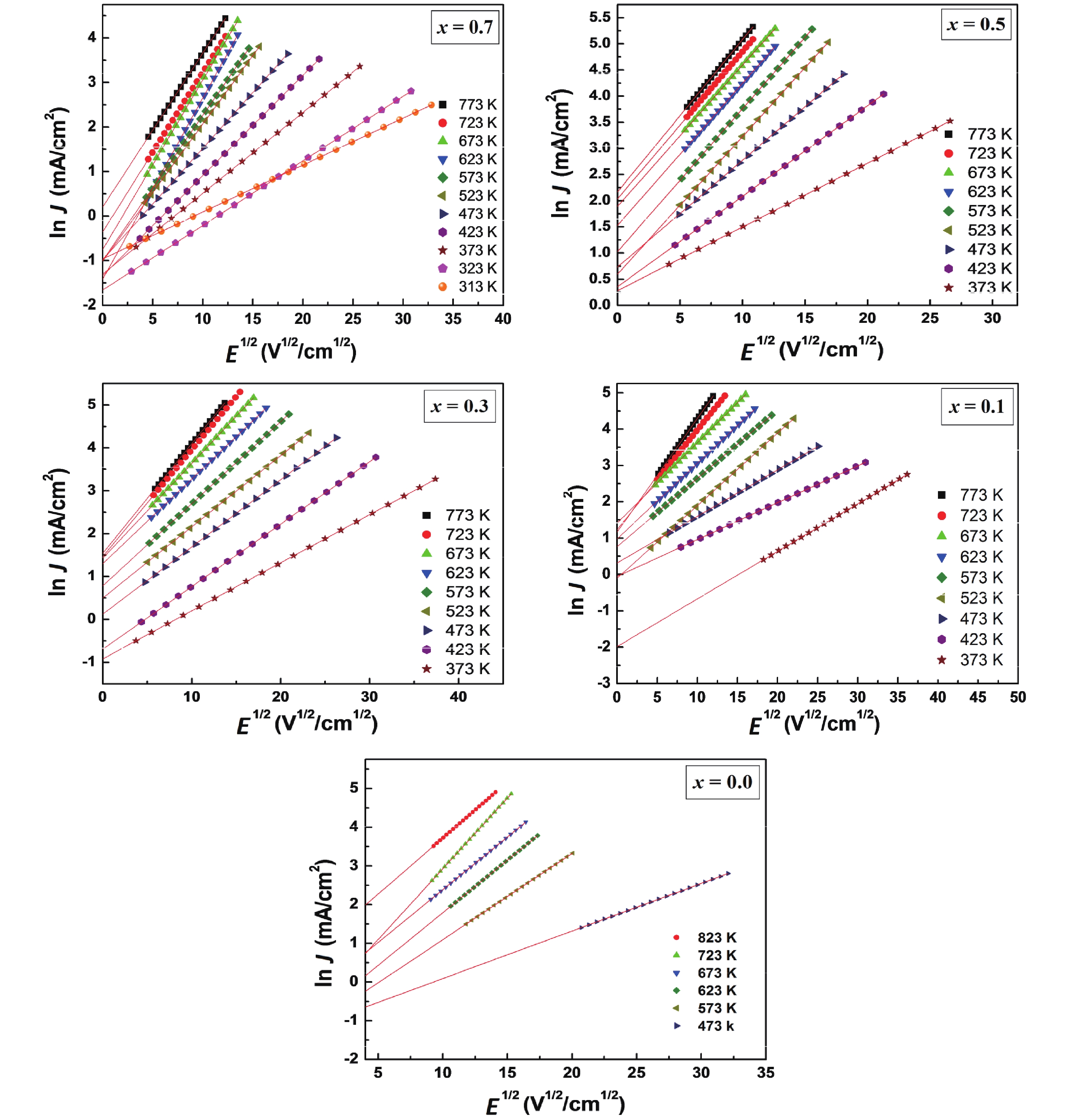
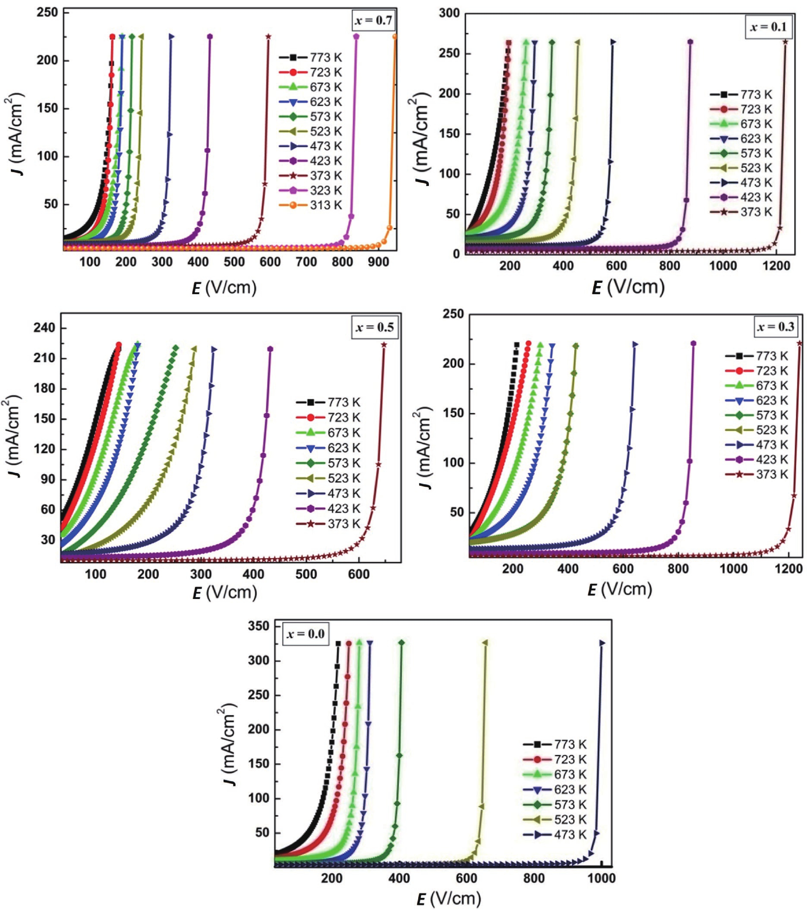
Fig. 1 gives the plots of J against E registered at different temperatures ranging from T = 300–773 K for the series CaCu3–xTi4–xFe2xO12. The samples exhibit strong non-ohmic characteristics. In the low E region, the dominant conduction mechanism is thermal excitation and as a result the J–E curve is nearly ohmic. Nonlinear behavior is observed when E is beyond the particular threshold value or breakdown value (Es) (E > Es). In this regime, tunneling action via grain-boundary barrier is responsible for the electric conduction. It is seen in Fig. 1 that the lowest temperature at which switching action takes place (TsL) decreases with Fe-content (x). The compositions with x = 0.0, (0.1, 0.3, 0.5) and 0.7 show switching action for T ≥ 473 K, (T ≥ 373 K), T ≥ 313 K, respectively. Meanwhile, Es decreases with x for x = 0.0 to 0.5 compositions, while for x = 0.7 composition Es shows small enhancement (Table 1). The compositional variation of Es may be described by considering the structural and microstructural parameters. The strain values have been deduced from the simple and widely employed Williamson-Hall plot method[38]. The negative slope for all of the compositions suggests that a compressive strain has been produced (Fig. 2). The strain increases from –4.54 × 10⁻⁴ for x = 0.0 composition to –6.77 × 10⁻⁴ for x = 0.3 composition, it then decreases to –5.96 × 10⁻⁴ for x = 0.5 composition and further increases to –6.95 × 10⁻⁴ for x = 0.7 composition. It has been reported elsewhere that strain is directly proportional to TsL and Es, values[26] but no such correlation has been observed in this work. Hu et al.[39] have shown that for ceramically prepared compositions, Es is inversely proportional to aggregate grain size (D) (Es


Another interesting observation from Fig. 1 is that maximum current density (Jmax) decreases from 327 mA/cm2 for x = 0.0 composition to 270 mA/cm2 for x = 0.1 composition to 225 mA/cm2 for x = 0.3 composition and remains constant with further Fe3+-substitution. In the design of electronic and electrical devices, current density has a very significant role. Over the last few years, there has been a movement towards having a higher current density to achieve a higher number of devices in an ever-smaller chip area. As discussed earlier, with an increase in D for x = 0.0–0.5 compositions, the contribution from poorly conducting grain boundaries decreases as compared to semiconducting grains; thus, Jmax is expected to increase with Fe- substitution, but this is not the case. This suggests that besides grain size, other microstructural parameters are also expected to affect Jmax. Zheng et al.[40], following the density functional theory, have shown that in CaCu3Ti4O12 the conduction mechanism is an adiabatic hopping conduction of small polarons and electron transport among CuO4 square-planar (A´-site) clusters. Furthermore, the conduction band is chiefly contributed by the antibonding states of Cu 3d electrons. Usually, metal oxide series containing Jahn-Teller ions (high-spin d4 Cr2+ and Mn3+ ions, low-spin d7 Co2+ and d9 Cu2+ ions) are referred to as the most likely candidates to demonstrate switching action. Based on the above findings, it is clear that cupric ions on the A´-site play a governing role in switching phenomenon and electric conduction. It is now feasible to elucidate the compositional variation of Jmax. The occupancy of metallic cations such as Ca2+, Cu2+, Ti4+ and Fe3+ among the crystallographic interstitial sites determined from Rietveld refinement of X-ray diffraction patterns revealed that with Fe- substitution the Cu2+-ion concentration at the A´ decreases from 3.0 for x = 0.0 composition to 1.53 for x = 0.7 composition[29, 33], as displayed in Table 2. This results in the curtailment of electric conduction through the square-planar site, and thus Jmax decreases rapidly for x = 0.0–0.3 compositions and then levels off for the compositions with x = 0.5 and 0.7, as shown in Table 1. The observed reduction in Jmax for x = 0.7 composition can also be explained based on the formation of a minor secondary insulating TiO2-phase and reduced grain size. The percentage formation of these secondary phases is well below the theoretical percolation threshold (~16%) and experimental percolation threshold (~20%) values. This would ensure that electric behavior such as Es and Jmax would always be dominated by the CaCu3Ti4O12 phase[33]. An effort has been undertaken to correlate the previous outcome of the PAL spectroscopy study[29] and present electric parameters as a function of composition (x). The magnitude of defect-specific positron lifetime (τ2) reflects the contributions from the grain boundaries, vacancies, and vacancy clusters in grains. Earlier, it was found that τ2 gradually increases from 0.2317 ns for x = 0.0 composition to 0.4449 ns for x = 0.5 composition and then level off for x = 0.7 composition to 0.4379 ns. The subsequent increase in τ2 suggests that the thickness of grain-boundary layers increases with Fe-substitution for x = 0.0–0.5 compositions and saturate for x = 0.7 compositions. This limits the conduction of charge carriers from one conducting grain to the adjacent conducting grain separated by the highly resistive grain boundary. This is thought to be the cause of the observed initial reduction of Jmax with x. On the same line of argument, Es is expected to increase with x but no such trend has been observed. This suggests that as far as Es value is concerned, an increase in grain size and decrease in defect density in grains dominant over the grain boundary broadening with Fe3+- substitution in the system, CaCu3–xTi4–xFe2xO12.
To the best of our knowledge, these values of Jmax for the pure and Fe-substituted CaCu3Ti4O12 ceramics are the highest ever reported values, except for those reported for Nb5+ and Ta5+-substituted CaCu3Ti4O12 (Jmax ≈ 275 mA/cm2)[41]. Earlier, we have found Jmax = 254 mA/cm2 and 234 mA/cm2 for quenched and microwave-assisted samples of CaCu3Ti4O12, respectively[26]. The nanocrystalline and microcrystalline samples of CaCu3Ti4O12 synthesized by distinct routes (solid-state reaction, sol-gel, modified sol-gel, thermal decomposition, spark plasma sintering etc.) and treated with different conditions (atmoshphere, sintering temperature and duration etc.) have shown that Jmax varies from 0.1–32 mA/cm2[3, 42-48]. Meanwhile, Y and Mg co-doped samples of CaCu3Ti4O12 have shown Jmax ≈ 28 mA/cm2[49], Sr-Ni substituted CaCu3Ti4O12 have exhibited Jmax ≈ 15 mA/cm2[14], Pr-substituted CaCu3Ti4O12 have demonstrated Jmax = 15 mA/cm2[50], while Zn + Zr co-doped CaCu3Ti4O12 thin films show Jmax in the range of 5–6 mA/cm2[51]. Finally, the composites, (1–x) (CaCu3Ti4O12)–(x)(0.1 Na0.5 Bi0.5TiO3–0.9 BaTiO3) with x = 0.02, 0.04, 0.06, 0.08 and 0.10, have shown Jmax ranging from 13–20 mA/cm2[52].
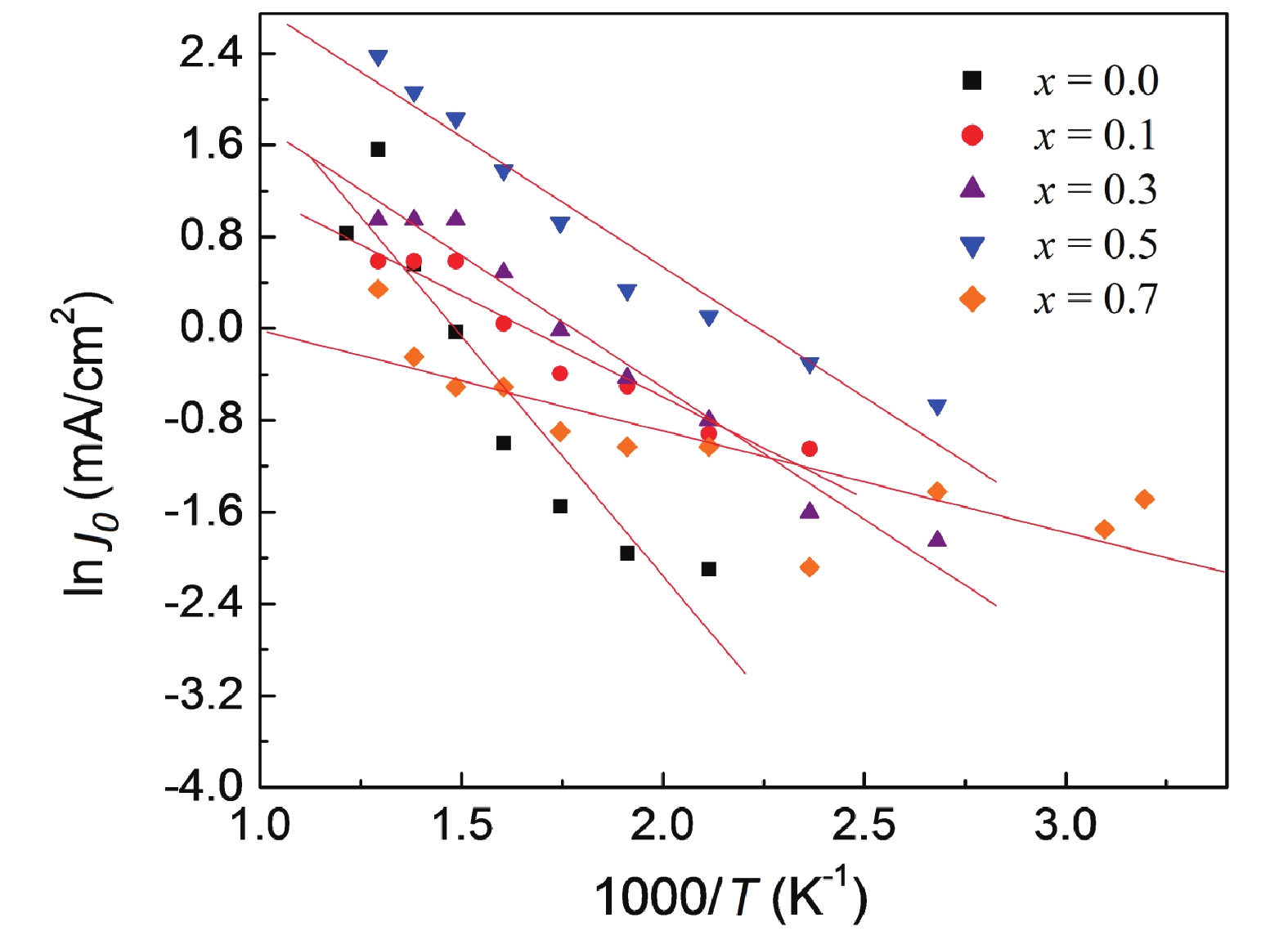
The existence of the Schottky barrier at the grain boundaries is signified by the observed linear relationship for ln J against E1/2 traces[53–55] (Fig. 3). The Schottky barrier height (ϕB) values determined from the slopes of the fitting lines of ln J0 (J0 is the value of J extrapolated to E = 0 V/cm) against reciprocal of temperature 1000/T graphs (Fig. 4) decreases from 0.25 eV for x = 0.0 composition to 0.21 eV for x = 0.5 composition while ϕB value increases to 0.28 eV for x = 0.7 compositions. The electric potential barrier height for the pristine composition, CaCu3Ti4O12 is consistent with the reported value[56]. Huang et al.[54] have shown that the ϕB is influenced by the residual impurities and impurities from decomposition. The ϕB demonstrates a close linear relationship to the microstrain and δ.

The coefficient of determination (R2) of a statistical model describes how well it fits a set of observations. A measure of this goodness-of-fit typically summarizes the discrepancy between the observed values and the values expected under the model in question. The R2 value between 0.70–1.0 indicates that there is a strong correlation between the dependent and independent variables. In general, R2 value at or above 0.60 is considered to be worthwhile[57].
On fitting ln J0 versus reciprocal of temperature (1000/T) plots with linear relation, the R2 value for x = 0.0 composition is found to be 0.91, for x = 0.1 composition, R2 = 0.94, for x = 0.3 composition, R2 = 0.97, for x = 0.5 composition, R2 = 0.95 and for the composition with x = 0.7, R2 comes to 0.90. These values of R2 are near the ideal value of 1.0, which suggests that the applied carrier transport model is able to successfully and accurately model the experimental data.
When we think about the varistor-type device, two parameters (i.e., non-linearity coefficient (α) and Es) are considered as a figure-of-merit. A large value of α is always desirable because it allows the device to withstand the surges at Es. The α values at different temperatures were calculated for the compositions with x = 0.0–0.7 using the standard definition. The α value is found to vary from 2.09–4.51, 0.45–1.14, 0.60–1.64, 0.76–2.34, and 1.27–6.88 for x = 0.0, 0.1, 0.3, 0.5 and 0.7 compositions, respectively, in the studied range of temperature. Furthermore, the value of α is found to increase with temperature and Fe-substitution (x) (x = 0.1–0.7). This can be explained as follows.
The nonlinear coefficient (

The high-temperature synthesis process of oxide ceramics that is employed here leads to the inevitable formation and existence of pores. Thus, X-ray density (dx) is always higher than the bulk density (d). These voids decisively affect the electric, dielectric, and elastic properties of the material. Thus, it is essential to correct such parameters for a void-free state, especially for compositional dependent investigation. The dc resistivity values in the void-free state (ρdc) for the different compositions have been determined from the experimental values of dc resistivity (ρp) recorded at different temperatures and void fraction values (f = 1 – (d/dx)) with the help of the following relation [59] ׃
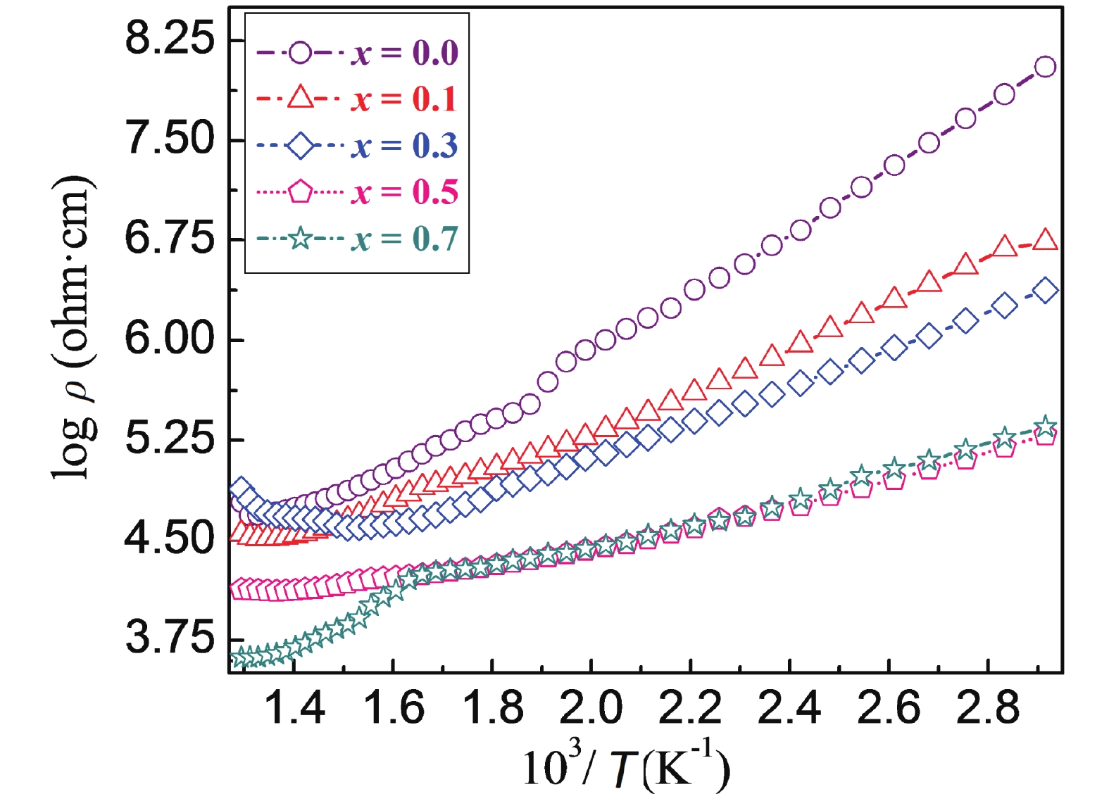
| ρdc=ρp[1+f(1+f2/3)−1]−1, |

This relation is effectively applied for the materials having f < 0.4. The different compositions of the system under study possess f values that are much less than 0.4, as shown in Table 1. The ρdc values for x = 0.0–0.7 compositions lie in the range105–108 Ω·cm at T = 300 K, advising that these are good insulating materials. Fig. 5 portrays log ρ versus temperature plots (Arrhenius plot). All of the compositions reveal usual semiconducting behavior (i.e., a decrease of resistivity with temperature). In the low-temperature regime, 300 K ≤ T ≤ 573 K, a linear variation of resistivity with temperature is observed; while for T > 573 K, a discontinuity or change of slope occurs, suggesting a change in the mechanism responsible for conduction in the studied materials. This may be correlated with the diffuse anomaly that takes place at T = 630 K[60] or may be associated with high-temperature structural phase transition reported occurring between T = 726–732 K for pure CaCu3Ti4O12 composition[61]. The activation energy values (Ea1 and Ea2) were calculated for regions below and above the transition temperature, respectively, from the well-known Arrhenius equation and are shown in Table 1. In the low-temperature region, T = 300–573 K, Ea1 decreases from 0.33 eV for x = 0.0 composition to 0.22 eV for x = 0.3 composition, and then increases to 0.25 and 0.27 eV for x = 0.5 and 0.7 compositions, respectively. The lattice constant (a) value decreases from 7.391 Å for x = 0.0 composition to 7.387 Å for x = 0.3 composition, and then increases to 7.400 and 7.411 Å for x = 0.5 and 0.7 compositions, respectively (Table 1). The observed reduction in a with x suggests a corresponding decrease in interionic distances and as a result a decrease in barrier height encountered by the hopping charge carriers. Thus, Ea1 is supposed to decrease for x = 0.0–0.3 compositions. The same argument is applicable for the observed increase in Ea1 with an increase in a for x = 0.5 and 0.7 compositions. The average size of grains (D) also affects Ea1[62]. A bigger grain size insinuates increased grain-to-grain contact area for the charge carrier to flow and consequently a lower barrier height, and vice versa. As discussed above, D increases from 3.7 μm for x = 0.0 composition to 7.9 μm for x = 0.5 composition and then decrease to 3.4 μm for x = 0.7 composition. This explains the observed dependence of Ea1 with Fe-content (x). The Ea1 values ranging from 0.22–0.33 eV are much higher than the ionization energy of acceptors and donors (i.e., 0.1 eV), and thus band-type conduction may not be possible. These values lie between the activation energy of a small polaron (≥ 0.5 eV) and the energy needed for the electron hopping mechanism (0.2 eV). Thus, the conduction proceeds by electrons with deformation. The Ea2 for the high-temperature regime are 0.43, 0.29, 0.21, 0.15, 0.21 eV, respectively, for x = 0.0, 0.1, 0.3, 0.5 and 0.7 compositions. Commonly, the resistivity of oxide ceramics is essentially dependent on the mobility and concentration of the carrier, but at such relatively low temperature it cannot be ascribed to oxygen depletion or absorption. The observed high-temperature deviation may be the result of the vacancy-disorder transition. Oxygen vacancies become ordered in the low-temperature regime, considerably enhancing the resistivity and thus higher activation energy. In the high-temperature regime, the conduction process is contributed by the oxygen ions and the oxygen vacancies are disordered, which allows oxygen ions to migrate with lower activation energy[25]. Furthermore, in the temperature range studied, resistivity decreases with Fe3+-concentration (x). The incorporation of highly magnetic Fe3+ ions which take part in the process of conduction, for non-magnetic Ti4+ ions, enhances the degree of Fe3+ + e– = Fe2+ conduction that occurs on the A´ - site of the cubic perovskite structure. Thus, dc resistivity decreases with Fe3+-substitution.
4. Conclusions
The following conclusions can be drawn based on the electrical properties studies of a series of quadruple perovskites, CaCu3–xTi4–xFe2xO12 where x = 0.0–0.7. The switching action is chiefly due to the concentration of Jahn-Teller Cu2+ ion engendered distortion in the system. The variation of switching temperature and threshold field is principally governed by grain size, interface defect density, and vacancy defects but not by compressive strain. The Jmax value is controlled by a change in Cu2+ ion concentration on the A´-site and the thickness of the grain-boundary layer on Fe3+-substitution. It is possible to tailor electrical parameters by controlling the structural and microstructural parameters, which is important from an application's point of view. The system is found to be suitable for low-voltage varistor applications. The compositional dependence of dc resistivity is governed by ferric ion concentration on the square-planar site of cubic perovskite structure and the activation energy values are suggestive of conduction through electrons with deformation.
Acknowledgements
One of the authors (DJP) is thankful to the Education Department, Gujarat state for providing financial assistance under ScHeme of developing high-quality research (SHODH).
 DownLoad: