


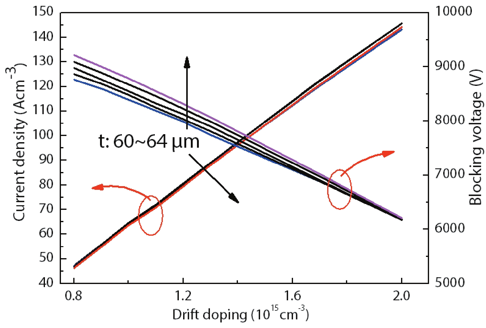
Fig. 1.
(Color online) Current density and blocking voltage variation with doping concentration and thickness of epitaxial layer.
ARTICLES
Lixin Tian1, , Zechen Du1, Rui Liu1, Xiping Niu1, Wenting Zhang1, Yunlai An1, Zhanwei Shen2, Fei Yang1, and Xiaoguang Wei1
Corresponding author: Lixin Tian, tianlixin0526@163.com; Fei Yang, yangsenji@163.com
Abstract: Silicon carbide (SiC) material features a wide bandgap and high critical breakdown field intensity. It also plays an important role in the high efficiency and miniaturization of power electronic equipment. It is an ideal choice for new power electronic devices, especially in smart grids and high-speed trains. In the medium and high voltage fields, SiC devices with a blocking voltage of more than 6.5 kV will have a wide range of applications. In this paper, we study the influence of epitaxial material properties on the static characteristics of 6.5 kV SiC MOSFET. 6.5 kV SiC MOSFETs with different channel lengths and JFET region widths are manufactured on three wafers and analyzed. The FN tunneling of gate oxide, HTGB and HTRB tests are performed and provide data support for the industrialization process for medium/high voltage SiC MOSFETs.
Key words: silicon carbide, epitaxial layer, channel length, JFET region width, FN tunneling, HTGB
| [1] |
Sun B X, Xie R B, Yu C, et al. Structural characterization of SiC nanoparticles. J Semicond, 2017, 38, 103002 doi: 10.1088/1674-4926/38/10/103002
|
| [2] |
Zeng C, Deng L F, Li Z J, et al. Experimental comparison of SiC GTO and ETO for pulse power applications. J Semicond, 2018, 39, 124017 doi: 10.1088/1674-4926/39/12/124017
|
| [3] |
Wolfspeed company C4D40120D datasheet [EB/OL] (2019-6-17) [2020-3-2]. https://www.wolfspeed.com/power/products/sic-schottky-diodes
|
| [4] |
Rohm company SCT2450KEHR datasheet [EB/OL] (2019-2-22). https://www.rohm.com.cn/products/sic-power-devices/sic-mosfet
|
| [5] |
Infineon company AIMW120R035M1H datasheet [EB/OL] (2019-2-22). https://www.infineon.com/cms/cn/product/power/mosfet/silicon-carbide/discretes/aimw120r035m1h
|
| [6] |
Mainali K, Wang R X, Sabate J, et al. Current sharing and overvoltage issues of paralleled SiC MOSFET modules. 2019 IEEE Energy Convers Congr Expo ECCE, 2019, 2413 doi: 10.1109/ECCE.2019.8912526
|
| [7] |
Chen J J, Jiang X, Li Z J, et al. Investigation on effects of thermal stress on SiC MOSFET degradation through power cycling tests. 2020 IEEE Applied Power Electronics Conference and Exposition, 2020, 1106 doi: 10.1109/APEC39645.2020.9124249
|
| [8] |
Bencherif H, Yousfi A, Dehimi L, et al. Analysis of Al2O3 high-k gate dielectric effect on the electrical characteristics of a 4H-SiC low-power MOSFET. 2019 1st International Conference on Sustainable Renewable Energy Systems and Applications, 2019, 1 doi: 10.1109/ICSRESA49121.2019.9182412
|
| [9] |
Wirths S, Mihaila A, Romano G, et al. Study of 1.2kV high-k SiC power MOSFETS under harsh repetitive switching conditions. 2021 33rd International Symposium on Power Semiconductor Devices and ICs, 2021, 107 doi: 10.23919/ISPSD50666.2021.9452286
|
| [10] |
Fukunaga S, Takayama H, Hikihara T. A study on switching surge voltage suppression of SiC MOSFET by digital active gate drive. 2021 IEEE 12th Energy Conversion Congress & Exposition, 2021 doi: 10.1109/ECCE-Asia49820.2021.9479030
|
| [11] |
Agarwal A, Baliga B J, Francois M M A, et al. 3.3 kV 4H-SiC planar-gate MOSFETs manufactured using Gen-5 PRESiCE™ technology in a 4-inch wafer commercial foundry. Southeastcon 2021, 2021, 1 doi: 10.1109/SoutheastCon45413.2021.9401931
|
| [12] |
Konstantinov A O, Wahab Q, Nordell N, et al. Ionization rates and critical fields in 4H silicon carbide. Appl Phys Lett, 1997, 71, 90 doi: 10.1063/1.119478
|
| [13] |
Tian L X, Yang F, Niu X P, et al. Development and analysis of 6500V SiC power MOSFET. 2021 18th China International Forum on Solid State Lighting & 2021 7th International Forum on Wide Bandgap Semiconductors, 2021, 6 doi: 10.1109/SSLChinaIFWS54608.2021.9675212
|
| [14] |
Chanana R K, McDonald K, di Ventra M, et al. Fowler-Nordheim hole tunneling in p-SiC/SiO2 structures. Appl Phys Lett, 2000, 77, 2560 doi: 10.1063/1.1318229
|
| [15] |
Fiorenza P, Frazzetto A, Guarnera A, et al. Fowler-Nordheim tunneling at SiO2/4H-SiC interfaces in metal-oxide-semiconductor field effect transistors. Appl Phys Lett, 2014, 105, 142108 doi: 10.1063/1.4898009
|
| [16] |
Karki U, Peng F Z. Precursors of gate-oxide degradation in silicon carbide MOSFETs. 2018 IEEE Energy Conversion Congress and Exposition, 2018, 857 doi: 10.1109/ECCE.2018.8557354
|
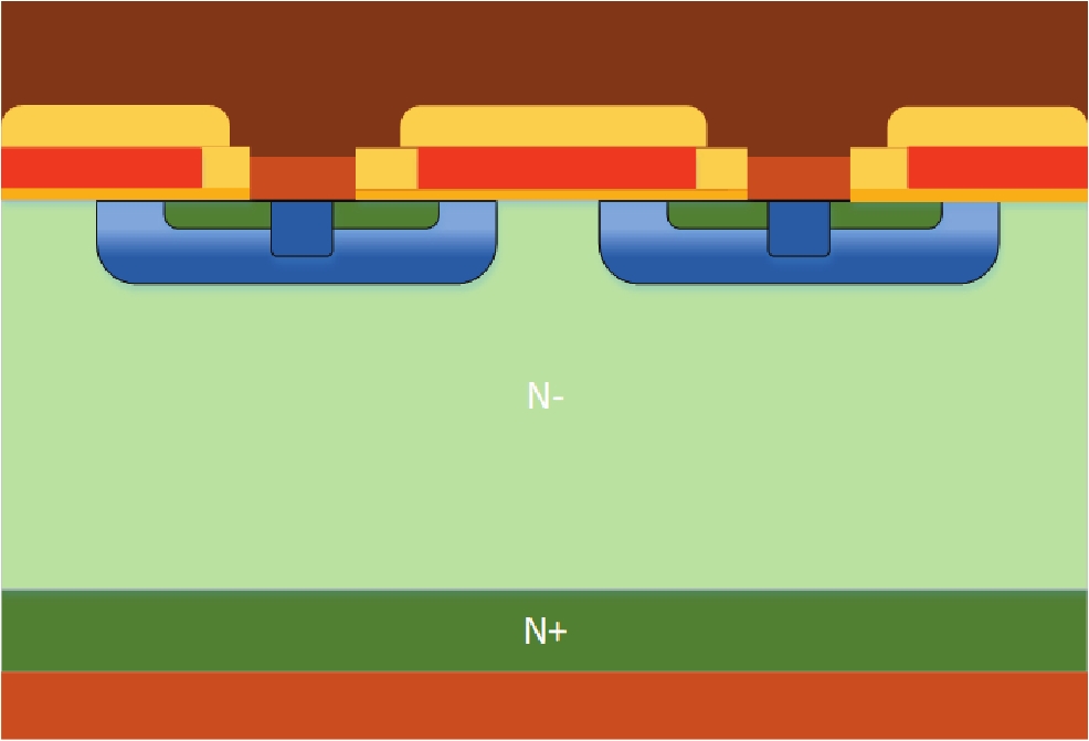
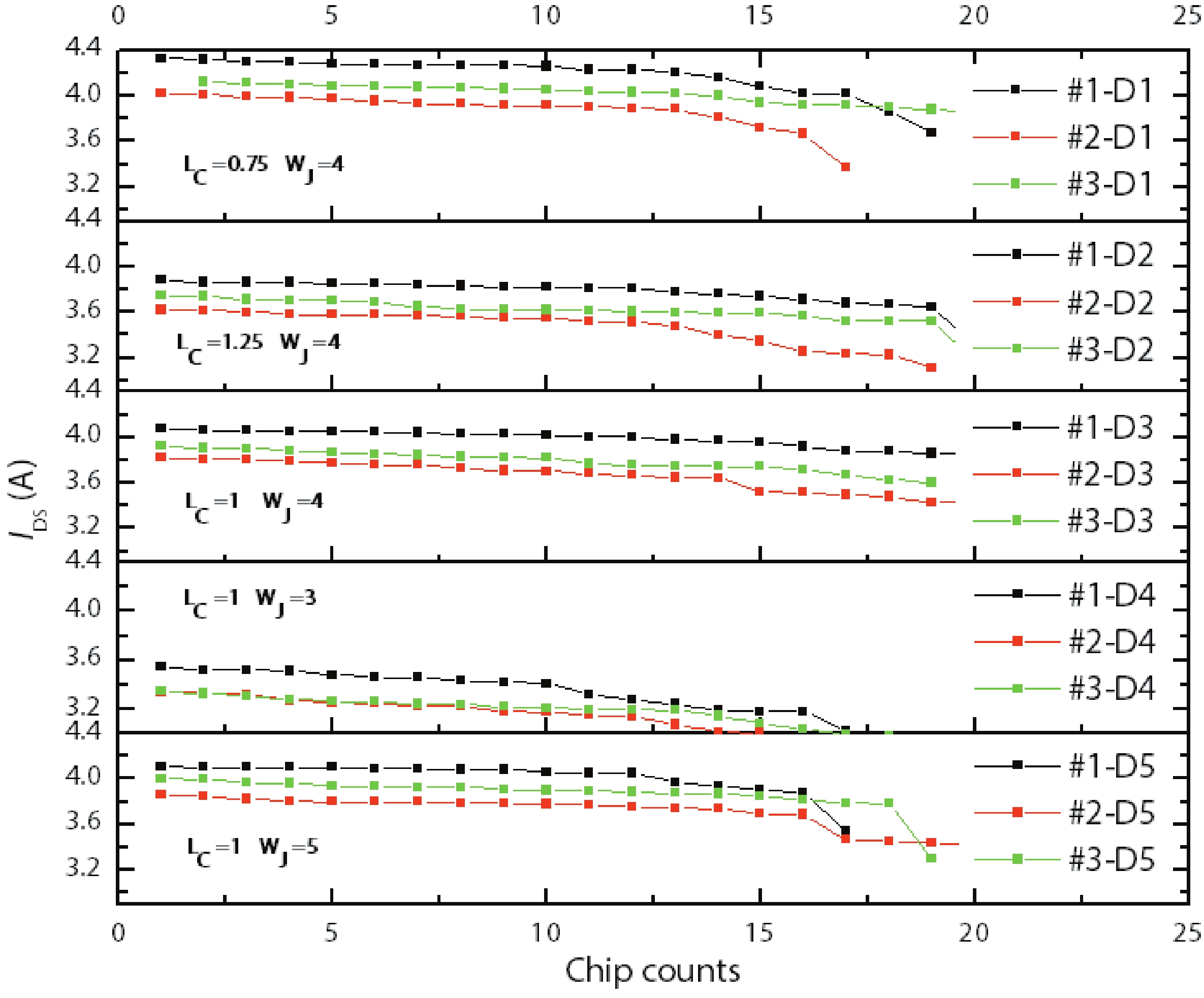
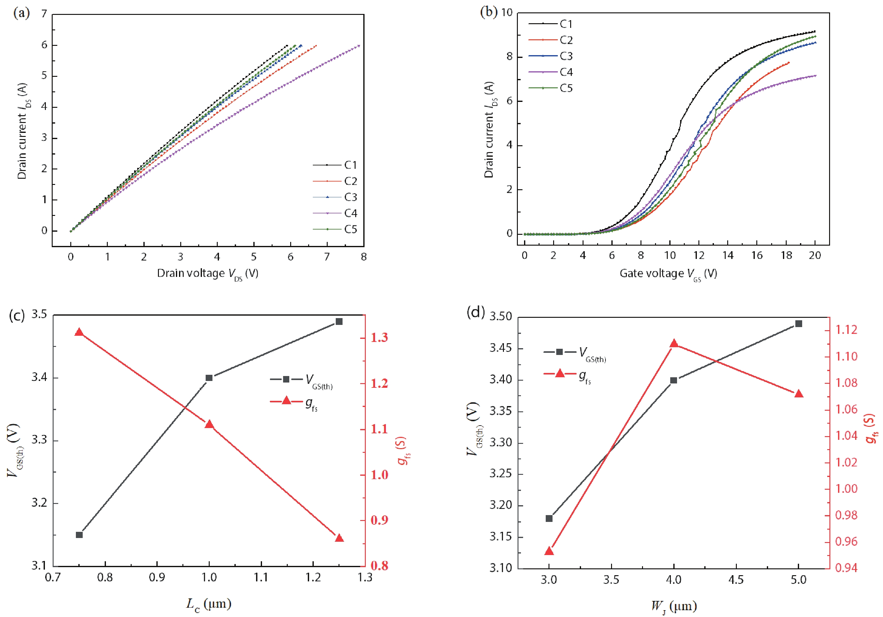
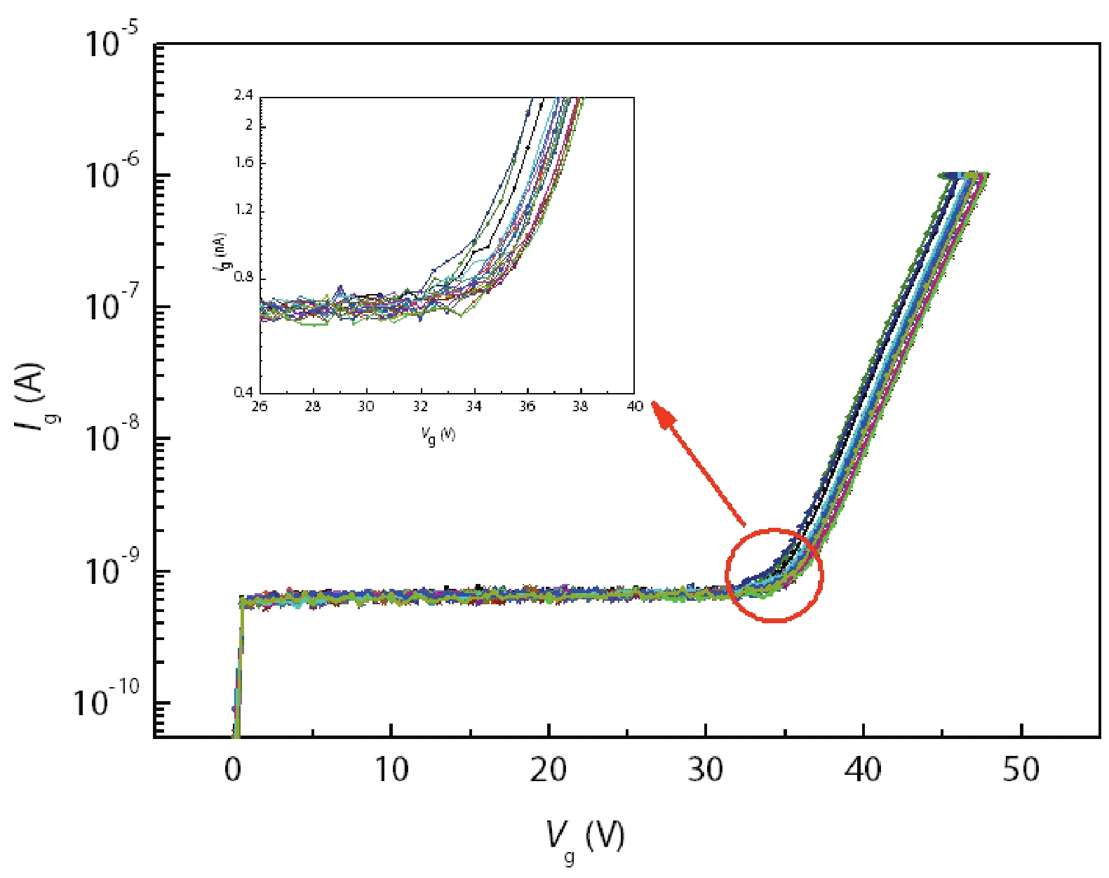
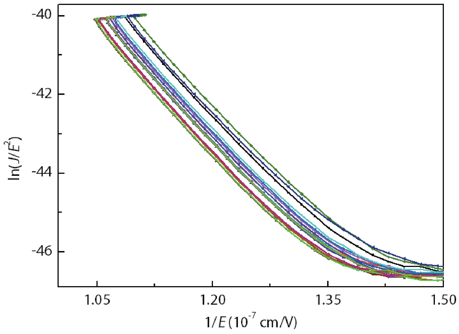
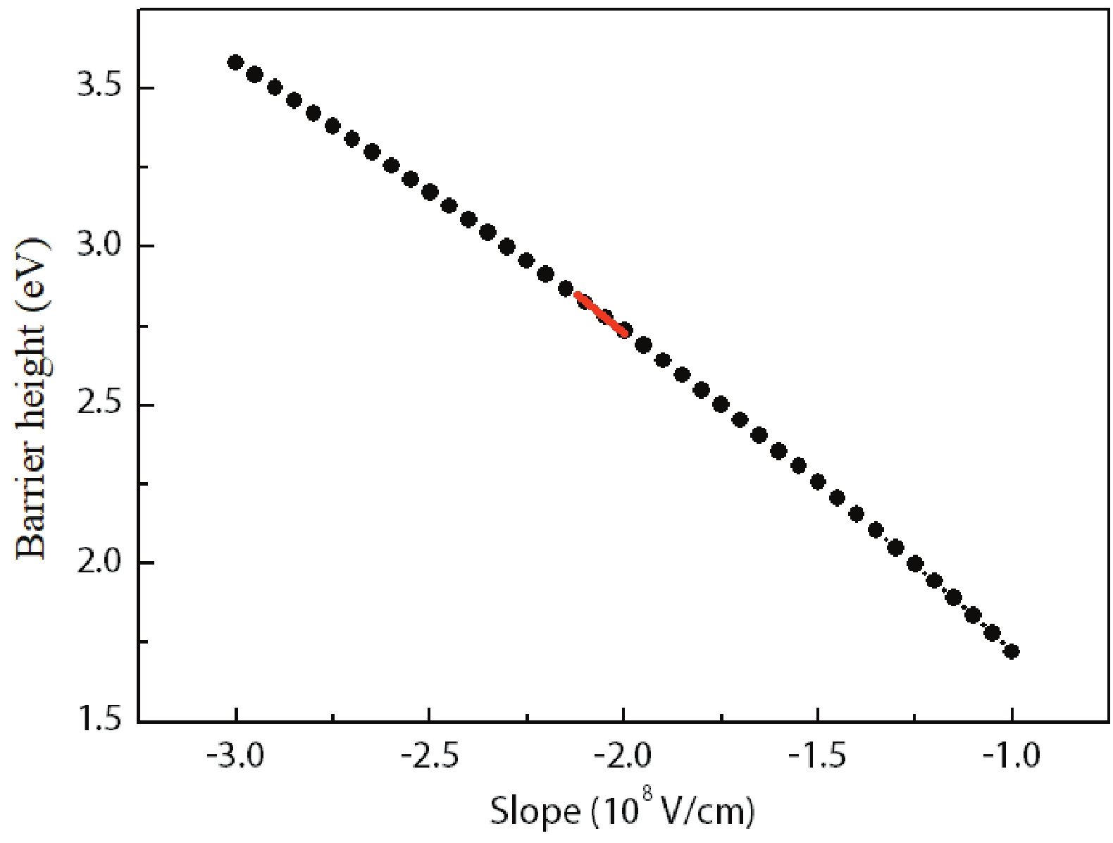
Table 1. Epitaxial layer thickness and doping concentration.
| Number | Thickness (μm) | Doping (1015 cm−3) | t/($N_{\rm d}q\mu$) |
| #1 | 64.7 | 1.29 | 34.1 |
| #2 | 62.3 | 1.16 | 36.5 |
| #3 | 62.5 | 1.22 | 34.8 |
 DownLoad: CSV
Table 2. Cell parameter table.
| Cell number | Channel length (μm) | Width of JFET region (μm) |
| C1 | 0.75 | 4 |
| C2 | 1.25 | 4 |
| C3 | 1 | 4 |
| C4 | 1 | 3 |
| C5 | 1 | 5 |
DownLoad: CSV
Table 3. Chip yield of 3 wafers.
| #1 | #2 | #3 | |
| C1 | 36.36% | 54.55% | 61.90% |
| C2 | 36.36% | 54.55% | 57.14% |
| C3 | 40.91% | 54.55% | 38.10% |
| C4 | 31.82% | 50.00% | 42.86% |
| C5 | 54.55% | 63.64% | 52.38% |
DownLoad: CSV
| [1] |
Sun B X, Xie R B, Yu C, et al. Structural characterization of SiC nanoparticles. J Semicond, 2017, 38, 103002 doi: 10.1088/1674-4926/38/10/103002
|
| [2] |
Zeng C, Deng L F, Li Z J, et al. Experimental comparison of SiC GTO and ETO for pulse power applications. J Semicond, 2018, 39, 124017 doi: 10.1088/1674-4926/39/12/124017
|
| [3] |
Wolfspeed company C4D40120D datasheet [EB/OL] (2019-6-17) [2020-3-2]. https://www.wolfspeed.com/power/products/sic-schottky-diodes
|
| [4] |
Rohm company SCT2450KEHR datasheet [EB/OL] (2019-2-22). https://www.rohm.com.cn/products/sic-power-devices/sic-mosfet
|
| [5] |
Infineon company AIMW120R035M1H datasheet [EB/OL] (2019-2-22). https://www.infineon.com/cms/cn/product/power/mosfet/silicon-carbide/discretes/aimw120r035m1h
|
| [6] |
Mainali K, Wang R X, Sabate J, et al. Current sharing and overvoltage issues of paralleled SiC MOSFET modules. 2019 IEEE Energy Convers Congr Expo ECCE, 2019, 2413 doi: 10.1109/ECCE.2019.8912526
|
| [7] |
Chen J J, Jiang X, Li Z J, et al. Investigation on effects of thermal stress on SiC MOSFET degradation through power cycling tests. 2020 IEEE Applied Power Electronics Conference and Exposition, 2020, 1106 doi: 10.1109/APEC39645.2020.9124249
|
| [8] |
Bencherif H, Yousfi A, Dehimi L, et al. Analysis of Al2O3 high-k gate dielectric effect on the electrical characteristics of a 4H-SiC low-power MOSFET. 2019 1st International Conference on Sustainable Renewable Energy Systems and Applications, 2019, 1 doi: 10.1109/ICSRESA49121.2019.9182412
|
| [9] |
Wirths S, Mihaila A, Romano G, et al. Study of 1.2kV high-k SiC power MOSFETS under harsh repetitive switching conditions. 2021 33rd International Symposium on Power Semiconductor Devices and ICs, 2021, 107 doi: 10.23919/ISPSD50666.2021.9452286
|
| [10] |
Fukunaga S, Takayama H, Hikihara T. A study on switching surge voltage suppression of SiC MOSFET by digital active gate drive. 2021 IEEE 12th Energy Conversion Congress & Exposition, 2021 doi: 10.1109/ECCE-Asia49820.2021.9479030
|
| [11] |
Agarwal A, Baliga B J, Francois M M A, et al. 3.3 kV 4H-SiC planar-gate MOSFETs manufactured using Gen-5 PRESiCE™ technology in a 4-inch wafer commercial foundry. Southeastcon 2021, 2021, 1 doi: 10.1109/SoutheastCon45413.2021.9401931
|
| [12] |
Konstantinov A O, Wahab Q, Nordell N, et al. Ionization rates and critical fields in 4H silicon carbide. Appl Phys Lett, 1997, 71, 90 doi: 10.1063/1.119478
|
| [13] |
Tian L X, Yang F, Niu X P, et al. Development and analysis of 6500V SiC power MOSFET. 2021 18th China International Forum on Solid State Lighting & 2021 7th International Forum on Wide Bandgap Semiconductors, 2021, 6 doi: 10.1109/SSLChinaIFWS54608.2021.9675212
|
| [14] |
Chanana R K, McDonald K, di Ventra M, et al. Fowler-Nordheim hole tunneling in p-SiC/SiO2 structures. Appl Phys Lett, 2000, 77, 2560 doi: 10.1063/1.1318229
|
| [15] |
Fiorenza P, Frazzetto A, Guarnera A, et al. Fowler-Nordheim tunneling at SiO2/4H-SiC interfaces in metal-oxide-semiconductor field effect transistors. Appl Phys Lett, 2014, 105, 142108 doi: 10.1063/1.4898009
|
| [16] |
Karki U, Peng F Z. Precursors of gate-oxide degradation in silicon carbide MOSFETs. 2018 IEEE Energy Conversion Congress and Exposition, 2018, 857 doi: 10.1109/ECCE.2018.8557354
|


Article views: 2355 Times PDF downloads: 157 Times Cited by: 0 Times
Received: 08 March 2022 Revised: 02 April 2022 Online: Accepted Manuscript: 26 May 2022Corrected proof: 27 May 2022Uncorrected proof: 30 May 2022Published: 01 August 2022
| Citation: |
Lixin Tian, Zechen Du, Rui Liu, Xiping Niu, Wenting Zhang, Yunlai An, Zhanwei Shen, Fei Yang, Xiaoguang Wei. Influence of epitaxial layer structure and cell structure on electrical performance of 6.5 kV SiC MOSFET[J]. Journal of Semiconductors, 2022, 43(8): 082802. doi: 10.1088/1674-4926/43/8/082802
****
L X Tian, Z C Du, R Liu, X P Niu, W T Zhang, Y L An, Z W Shen, F Yang, X G Wei. Influence of epitaxial layer structure and cell structure on electrical performance of 6.5 kV SiC MOSFET[J]. J. Semicond, 2022, 43(8): 082802. doi: 10.1088/1674-4926/43/8/082802

|
| [1] |
Sun B X, Xie R B, Yu C, et al. Structural characterization of SiC nanoparticles. J Semicond, 2017, 38, 103002 doi: 10.1088/1674-4926/38/10/103002
|
| [2] |
Zeng C, Deng L F, Li Z J, et al. Experimental comparison of SiC GTO and ETO for pulse power applications. J Semicond, 2018, 39, 124017 doi: 10.1088/1674-4926/39/12/124017
|
| [3] |
Wolfspeed company C4D40120D datasheet [EB/OL] (2019-6-17) [2020-3-2]. https://www.wolfspeed.com/power/products/sic-schottky-diodes
|
| [4] |
Rohm company SCT2450KEHR datasheet [EB/OL] (2019-2-22). https://www.rohm.com.cn/products/sic-power-devices/sic-mosfet
|
| [5] |
Infineon company AIMW120R035M1H datasheet [EB/OL] (2019-2-22). https://www.infineon.com/cms/cn/product/power/mosfet/silicon-carbide/discretes/aimw120r035m1h
|
| [6] |
Mainali K, Wang R X, Sabate J, et al. Current sharing and overvoltage issues of paralleled SiC MOSFET modules. 2019 IEEE Energy Convers Congr Expo ECCE, 2019, 2413 doi: 10.1109/ECCE.2019.8912526
|
| [7] |
Chen J J, Jiang X, Li Z J, et al. Investigation on effects of thermal stress on SiC MOSFET degradation through power cycling tests. 2020 IEEE Applied Power Electronics Conference and Exposition, 2020, 1106 doi: 10.1109/APEC39645.2020.9124249
|
| [8] |
Bencherif H, Yousfi A, Dehimi L, et al. Analysis of Al2O3 high-k gate dielectric effect on the electrical characteristics of a 4H-SiC low-power MOSFET. 2019 1st International Conference on Sustainable Renewable Energy Systems and Applications, 2019, 1 doi: 10.1109/ICSRESA49121.2019.9182412
|
| [9] |
Wirths S, Mihaila A, Romano G, et al. Study of 1.2kV high-k SiC power MOSFETS under harsh repetitive switching conditions. 2021 33rd International Symposium on Power Semiconductor Devices and ICs, 2021, 107 doi: 10.23919/ISPSD50666.2021.9452286
|
| [10] |
Fukunaga S, Takayama H, Hikihara T. A study on switching surge voltage suppression of SiC MOSFET by digital active gate drive. 2021 IEEE 12th Energy Conversion Congress & Exposition, 2021 doi: 10.1109/ECCE-Asia49820.2021.9479030
|
| [11] |
Agarwal A, Baliga B J, Francois M M A, et al. 3.3 kV 4H-SiC planar-gate MOSFETs manufactured using Gen-5 PRESiCE™ technology in a 4-inch wafer commercial foundry. Southeastcon 2021, 2021, 1 doi: 10.1109/SoutheastCon45413.2021.9401931
|
| [12] |
Konstantinov A O, Wahab Q, Nordell N, et al. Ionization rates and critical fields in 4H silicon carbide. Appl Phys Lett, 1997, 71, 90 doi: 10.1063/1.119478
|
| [13] |
Tian L X, Yang F, Niu X P, et al. Development and analysis of 6500V SiC power MOSFET. 2021 18th China International Forum on Solid State Lighting & 2021 7th International Forum on Wide Bandgap Semiconductors, 2021, 6 doi: 10.1109/SSLChinaIFWS54608.2021.9675212
|
| [14] |
Chanana R K, McDonald K, di Ventra M, et al. Fowler-Nordheim hole tunneling in p-SiC/SiO2 structures. Appl Phys Lett, 2000, 77, 2560 doi: 10.1063/1.1318229
|
| [15] |
Fiorenza P, Frazzetto A, Guarnera A, et al. Fowler-Nordheim tunneling at SiO2/4H-SiC interfaces in metal-oxide-semiconductor field effect transistors. Appl Phys Lett, 2014, 105, 142108 doi: 10.1063/1.4898009
|
| [16] |
Karki U, Peng F Z. Precursors of gate-oxide degradation in silicon carbide MOSFETs. 2018 IEEE Energy Conversion Congress and Exposition, 2018, 857 doi: 10.1109/ECCE.2018.8557354
|

 WeChat ID
Journal of Semiconductors © 2017 All Rights Reserved 京ICP备05085259号-2


