


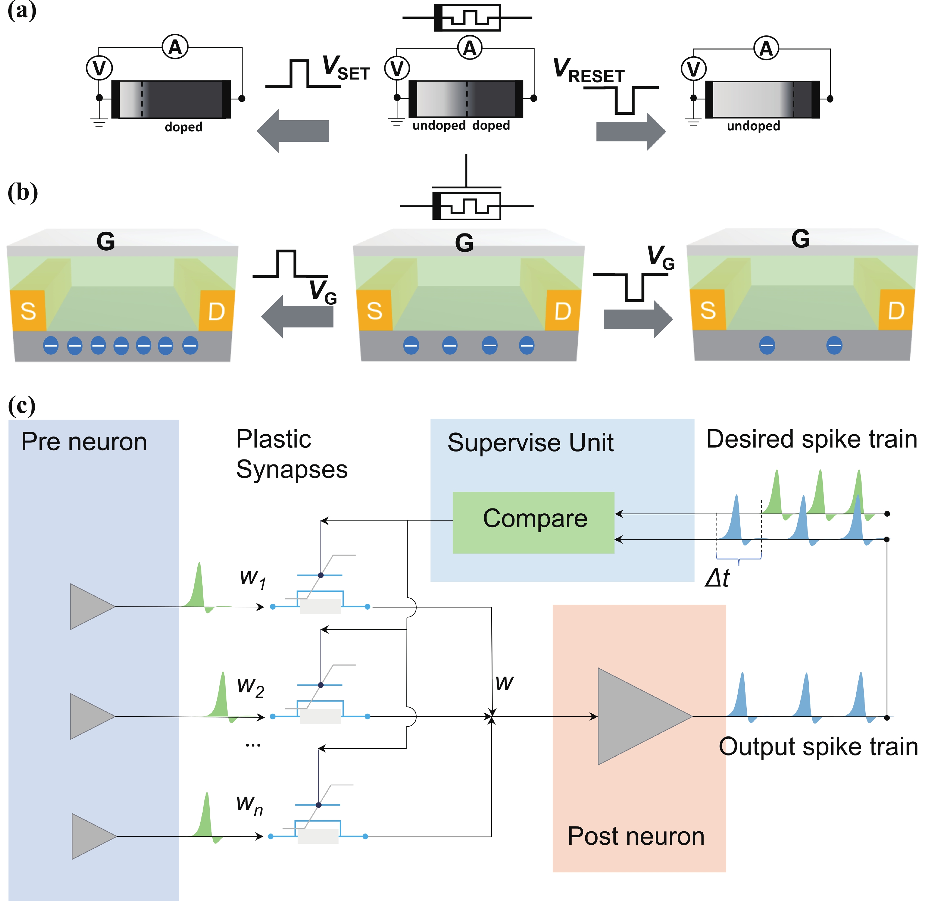
Fig. 1.
(Color online) Comparison of the nonvolatile conductance tuning in memristor (a) and in memtransistor (b) and the application of memtransistor in spiking neural network for concurrent forwarding and updating (c)[12].
REVIEWS
Qi Chen1, Yue Zhou2, Weiwei Xiong1, Zirui Chen3, 1, Yasai Wang4, 1, Xiangshui Miao1 and Yuhui He1,
Corresponding author: Yuhui He, heyuhui@hust.edu.cn
Abstract: Memtransistors in which the source−drain channel conductance can be nonvolatilely manipulated through the gate signals have emerged as promising components for implementing neuromorphic computing. On the other side, it is known that the complementary metal-oxide-semiconductor (CMOS) field effect transistors have played the fundamental role in the modern integrated circuit technology. Therefore, will complementary memtransistors (CMT) also play such a role in the future neuromorphic circuits and chips? In this review, various types of materials and physical mechanisms for constructing CMT (how) are inspected with their merits and need-to-address challenges discussed. Then the unique properties (what) and potential applications of CMT in different learning algorithms/scenarios of spiking neural networks (why) are reviewed, including supervised rule, reinforcement one, dynamic vision with in-sensor computing, etc. Through exploiting the complementary structure-related novel functions, significant reduction of hardware consuming, enhancement of energy/efficiency ratio and other advantages have been gained, illustrating the alluring prospect of design technology co-optimization (DTCO) of CMT towards neuromorphic computing.
Keywords: complementary memtransistor, neuromorphic computing, reward-modulated spike timing-dependent plasticity, remote supervise method, in-sensor computing
| [1] |
Chua L. Memristor-The missing circuit element. IEEE Transactions on Circuit Theory, 1971, 18(5), 507 doi: 10.1109/TCT.1971.1083337
|
| [2] |
Strukov D B, Snider G S, Stewart D R, et al. The missing memristor found. Nature, 2008, 453(7191), 80 doi: 10.1038/nature06932
|
| [3] |
Jo S H, Chang T, Ebong I, et al. Nanoscale memristor device as synapse in neuromorphic systems. Nano Lett, 2010, 10(4), 1297 doi: 10.1021/nl904092h
|
| [4] |
Alibart F, Zamanidoost E, Strukov D B. Pattern classification by memristive crossbar circuits using ex situ and in situ training. Nat Commun, 2013, 4, 2072 doi: 10.1038/ncomms3072
|
| [5] |
Yao P, Wu H, Gao B, et al. Face classification using electronic synapses. Nat Commun, 2017, 8, 15199 doi: 10.1038/ncomms15199
|
| [6] |
Wang Z R, Joshi S, Savel’ev S, et al. Fully memristive neural networks for pattern classification with unsupervised learning. Nat Electron, 2018, 1(2), 137 doi: 10.1038/s41928-018-0023-2
|
| [7] |
Cai F X, Correll J M, Lee S H, et al. A fully integrated reprogrammable memristor–CMOS system for efficient multiply–accumulate operations. Nat Electron, 2019, 2(7), 290 doi: 10.1038/s41928-019-0270-x
|
| [8] |
Yao P, Wu H Q, Gao B, et al. Fully hardware-implemented memristor convolutional neural network. Nature, 2020, 577(7792), 641 doi: 10.1038/s41586-020-1942-4
|
| [9] |
Sangwan V K, Lee H S, Bergeron H, et al. Multi-terminal memtransistors from polycrystalline monolayer molybdenum disulfide. Nature, 2018, 554(7693), 500 doi: 10.1038/nature25747
|
| [10] |
Yan X D, Qian J H, Sangwan V K, et al. Progress and challenges for memtransistors in neuromorphic circuits and systems. Adv Mater, 2022, 34(48), e2108025 doi: 10.1002/adma.202108025
|
| [11] |
Nishitani Y, Kaneko Y, Ueda M. Supervised learning using spike-timing-dependent plasticity of memristive synapses. IEEE Trans Neural Netw Learn Syst, 2015, 26(12), 2999 doi: 10.1109/TNNLS.2015.2399491
|
| [12] |
Chen Y Y, Zhou Y, Zhuge F W, et al. Graphene–ferroelectric transistors as complementary synapses for supervised learning in spiking neural network. NPJ 2D Mater Appl, 2019, 3(1), 31 doi: 10.1038/s41699-019-0114-6
|
| [13] |
Kim M K, Kim I J, Lee J S. CMOS-compatible ferroelectric NAND flash memory for high-density, low-power, and high-speed three-dimensional memory. Sci Adv, 2021, 7(3), eabe1341 doi: 10.1126/sciadv.abe1341
|
| [14] |
Liao J Y, Wen W, Wu J X, et al. Van der waals ferroelectric semiconductor field effect transistor for in-memory computing. ACS Nano, 2023, 17(6), 6095 doi: 10.1021/acsnano.3c01198
|
| [15] |
Wang H, Lu Y L, Liu S B, et al. Adaptive neural activation and neuromorphic processing via drain-injection threshold-switching float gate transistor memory. Adv Mater, 2023, 35, 2309099 doi: 10.1002/adma.202309099
|
| [16] |
Xiong X, Kang J Y, Hu Q L, et al. Reconfigurable logic-in-memory and multilingual artificial synapses based on 2D heterostructures. Adv Funct Materials, 2020, 30(11), 1909645 doi: 10.1002/adfm.201909645
|
| [17] |
Onen M, Emond N, Wang B M, et al. Nanosecond protonic programmable resistors for analog deep learning. Science, 2022, 377(6605), 539 doi: 10.1126/science.abp8064
|
| [18] |
Yan X D, Ma J H, Wu T, et al. Reconfigurable Stochastic neurons based on tin oxide/MoS2 hetero-memristors for simulated annealing and the Boltzmann machine. Nat Commun, 2021, 12(1), 5710 doi: 10.1038/s41467-021-26012-5
|
| [19] |
Sarwat S G, Kersting B, Moraitis T, et al. Phase-change memtransistive synapses for mixed-plasticity neural computations. Nat Nanotechnol, 2022, 17(5), 507 doi: 10.1038/s41565-022-01095-3
|
| [20] |
Shania R, Honggyun K, Farooq K M, et al. Tunable resistive switching of vertical ReSe2/graphene hetero-structure enabled by Schottky barrier height and DUV light. J Alloys Compd, 2021, 855, 157310 doi: 10.1016/j.jallcom.2020.157310
|
| [21] |
Ali T, Polakowski P, Riedel S, et al. High endurance ferroelectric hafnium oxide-based FeFET memory without retention penalty. IEEE Trans Electron Devices, 2018, 65(9), 3769 doi: 10.1109/TED.2018.2856818
|
| [22] |
Dünkel S, Trentzsch M, Richter R, et al. A FeFET based super-low-power ultra-fast embedded NVM technology for 22nm FDSOI and beyond. 2017 IEEE International Electron Devices Meeting (IEDM). San Francisco, CA, USA. IEEE, 2017, 19.7. 1 doi: 10.1109/IEDM.2017.8268425
|
| [23] |
Tanaka H, Kido M, Yahashi K, et al. Bit cost scalable technology with punch and plug process for ultra high density flash memory. 2007 IEEE Symposium on VLSI Technology. Kyoto, Japan. IEEE, 2007, 14 doi: 10.1109/VLSIT.2007.4339708
|
| [24] |
Kim K H, Song S, Kim B, et al. Tuning polarity in WSe2/AlScN FeFETs via contact engineering. ACS Nano, 2024, 18(5), 4180 doi: 10.1021/acsnano.3c09279
|
| [25] |
Chou Y C, Tsai C W, Yi C Y, et al. Neuro-inspired-in-memory computing using charge-trapping MemTransistor on germanium as synaptic device. IEEE Trans Electron Devices, 2020, 67(9), 3605 doi: 10.1109/TED.2020.3008887
|
| [26] |
Yao X H, Klyukin K, Lu W J, et al. Protonic solid-state electrochemical synapse for physical neural networks. Nat Commun, 2020, 11(1), 3134 doi: 10.1038/s41467-020-16866-6
|
| [27] |
Nikam R D, Kwak M, Hwang H. All-solid-state oxygen ion electrochemical random-access memory for neuromorphic computing. Adv Elect Materials, 2021, 7(5), 2100142 doi: 10.1002/aelm.202100142
|
| [28] |
Fuller E J, Gabaly F E, Léonard F, et al. Li-ion synaptic transistor for low power analog computing. Adv Mater, 2017, 29, 1604310 doi: 10.1002/adma.201604310
|
| [29] |
Song M K, Kang J H, Zhang X, et al. Recent advances and future prospects for memristive materials, devices, and systems. ACS Nano, 2023, 17(3), 11994 doi: 10.1021/acsnano.3c03505
|
| [30] |
Onen M, Emond N, Li J, et al. CMOS-compatible protonic programmable resistor based on phosphosilicate glass electrolyte for analog deep learning. Nano Lett, 2021, 21(14), 6111 doi: 10.1021/acs.nanolett.1c01614
|
| [31] |
Qian C, Kong L A, Yang J L, et al. Multi-gate organic neuron transistors for spatiotemporal information processing. Appl Phys Lett, 2017, 110(8), 083302 doi: 10.1063/1.4977069
|
| [32] |
Yang Y, Du H Y, Xue Q, et al. Three-terminal memtransistors based on two-dimensional layered gallium selenide nanosheets for potential low-power electronics applications. Nano Energy, 2018, 57, 566 doi: 10.1016/j.nanoen.2018.12.057
|
| [33] |
Iqbal S, Duy L T, Kang H, et al. Femtojoule-power-consuming synaptic memtransistor based on Mott transition of multiphasic vanadium oxides. Adv Funct Materials, 2021, 31(46), 2102567 doi: 10.1002/adfm.202102567
|
| [34] |
Zhou Y, Xu N, Gao B, et al. Complementary graphene-ferroelectric transistors (C-GFTs) as synapses with modulatable plasticity for supervised learning. 2019 IEEE International Electron Devices Meeting (IEDM). San Francisco, CA, USA. IEEE, 2019, 6.5. 1 doi: 10.1109/IEDM19573.2019.8993453
|
| [35] |
Markram H, Lübke J, Frotscher M, et al. Regulation of synaptic efficacy by coincidence of postsynaptic APs and EPSPs. Science, 1997, 275(5297), 213 doi: 10.1126/science.275.5297.213
|
| [36] |
Bi G Q, Poo M M. Synaptic modifications in cultured hippocampal neurons: Dependence on spike timing, synaptic strength, and postsynaptic cell type. J Neurosci, 1998, 18(24), 10464 doi: 10.1523/JNEUROSCI.18-24-10464.1998
|
| [37] |
Yuan J T, Liu S E, Shylendra A, et al. Reconfigurable MoS2 memtransistors for continuous learning in spiking neural networks. Nano Lett, 2021, 21(15), 6432 doi: 10.1021/acs.nanolett.1c00982
|
| [38] |
Nishitani Y, Kaneko Y, Ueda M, et al. Three-terminal ferroelectric synapse device with concurrent learning function for artificial neural networks. J Appl Phys, 2012, 111(12), 124108 doi: 10.1063/1.4729915
|
| [39] |
Zhai Y B, Xie P, Feng Z H, et al. 2D heterostructure for high-order spatiotemporal information processing. Adv Funct Materials, 2022, 32(7), 2108440 doi: 10.1002/adfm.202108440
|
| [40] |
Wang L, Liao W G, Wong S L, et al. Artificial synapses based on multiterminal memtransistors for neuromorphic application. Adv Funct Materials, 2019, 29(25), 1901106 doi: 10.1002/adfm.201901106
|
| [41] |
Leong J F, Fang Z H, Sivan M, et al. N-P reconfigurable dual-mode memtransistors for compact bio-inspired feature extractor with inhibitory-excitatory spiking capability. Adv Funct Materials, 2023, 33(45), 2302949 doi: 10.1002/adfm.202302949
|
| [42] |
Zhou Y, Xu N, Gao B, et al. Complementary memtransistor-based multilayer neural networks for online supervised learning through (anti-) spike-timing-dependent plasticity. IEEE Trans Neural Netw Learn Syst, 2022, 33(11), 6640 doi: 10.1109/TNNLS.2021.3082911
|
| [43] |
Shouval H Z, Wang S S H, Wittenberg G M. Spike timing dependent plasticity: A consequence of more fundamental learning rules. Front Comput Neurosci, 2010, 4, 19 doi: 10.3389/fncom.2010.00019
|
| [44] |
Ponulak F, Kasiński A. Supervised learning in spiking neural networks with ReSuMe: Sequence learning, classification, and spike shifting. Neural Comput, 2010, 22(2), 467 doi: 10.1162/neco.2009.11-08-901
|
| [45] |
Sporea I, Grüning A. Supervised learning in multilayer spiking neural networks. Neural Comput, 2013, 25(2), 473 doi: 10.1162/NECO_a_00396
|
| [46] |
Jerry M, Chen P Y, Zhang J C, et al. Ferroelectric FET analog synapse for acceleration of deep neural network training. 2017 IEEE International Electron Devices Meeting (IEDM), 2017, 6.2. 1 doi: 10.1109/IEDM.2017.8268338
|
| [47] |
Seo M, Kang M H, Jeon S B, et al. First demonstration of a logic-process compatible junctionless ferroelectric FinFET synapse for neuromorphic applications. IEEE Electron Device Lett, 2018, 39, 1445 doi: 10.1109/LED.2018.2852698
|
| [48] |
Woo J, Moon K, Song J, et al. Improved synaptic behavior under identical pulses using AlO x/HfO2 bilayer RRAM array for neuromorphic systems. IEEE Electron Device Lett, 2016, 37, 994 doi: 10.1109/LED.2016.2582859
|
| [49] |
Brzosko Z, Schultz W, Paulsen O. Retroactive modulation of spike timing-dependent plasticity by dopamine. eLife, 2015, 4, e09685 doi: 10.7554/eLife.09685
|
| [50] |
Florian R V. Reinforcement learning through modulation of spike-timing-dependent synaptic plasticity. Neural Comput, 2007, 19(6), 1468 doi: 10.1162/neco.2007.19.6.1468
|
| [51] |
Zhou Y, Wang Y S, Zhuge F W, et al. A reconfigurable two-WSe2-transistor synaptic cell for reinforcement learning. Adv Mater, 2022, 34(48), e2107754 doi: 10.1002/adma.202107754
|
| [52] |
Shi C, Lu J, Wang Y, et al. Exploiting memristors for neuromorphic reinforcement learning. 2021 IEEE 3rd International Conference on Artificial Intelligence Circuits and Systems (AICAS), 2021, 1 doi: 10.1109/AICAS51828.2021.9458542
|
| [53] |
Gerstner W, Kistler W M, Naud R, et al. Neuronal dynamics: From single neurons to networks and models of cognition. New York, NY: Cambridge University Press
|
| [54] |
Oh S, Hwang H, Yoo I K. Ferroelectric materials for neuromorphic computing. APL Mater, 2019, 7(9), 091109 doi: 10.1063/1.5108562
|
| [55] |
Chang T, Jo S H, Lu W. Short-term memory to long-term memory transition in a nanoscale memristor. ACS Nano, 2011, 5(9), 7669 doi: 10.1021/nn202983n
|
| [56] |
Zhou Y, Fu J W, Chen Z R, et al. Computational event-driven vision sensors for in-sensor spiking neural networks. Nat Electron, 2023, 6(11), 870 doi: 10.1038/s41928-023-01055-2
|
| [57] |
Zhou Y, Fu J W, Wan T Q, et al. A 2T2R1C vision cell with 140 dB dynamic range and event-driven characteristics for in-sensor spiking neural network. 2022 International Electron Devices Meeting (IEDM). San Francisco, CA, USA. IEEE, 2022, 31.4. 1 doi: 10.1109/IEDM45625.2022.10019350
|
| [58] |
Zhou F C, Chai Y. Near-sensor and in-sensor computing. Nat Electron, 2020, 3(11), 664 doi: 10.1038/s41928-020-00501-9
|
| [59] |
Mennel L, Symonowicz J, Wachter S, et al. Ultrafast machine vision with 2D material neural network image sensors. Nature, 2020, 579(7797), 62 doi: 10.1038/s41586-020-2038-x
|
| [60] |
Wan T Q, Shao B J, Ma S J, et al. In-sensor computing: Materials, devices, and integration technologies. Adv Mater, 2023, 35(37), e2203830 doi: 10.1002/adma.202203830
|
| [61] |
Yang Y K, Pan C, Li Y X, et al. In-sensor dynamic computing for intelligent machine vision. Nat Electron, 2024 doi: 10.1038/s41928-024-01124-0
|
| [62] |
Bichler O, Querlioz D, Thorpe S J, et al. Extraction of temporally correlated features from dynamic vision sensors with spike-timing-dependent plasticity. Neural Netw, 2012, 32, 339 doi: 10.1016/j.neunet.2012.02.022
|
| [63] |
Bichler O, Suri M, Querlioz D, et al. Visual pattern extraction using energy-efficient "2-PCM synapse" neuromorphic architecture. IEEE Trans Electron Devices, 2012, 59(8), 2206 doi: 10.1109/TED.2012.2197951
|
| [64] |
Kim Y, Panda P. Optimizing deeper spiking neural networks for dynamic vision sensing. Neural Netw, 2021, 144, 686 doi: 10.1016/j.neunet.2021.09.022
|
| [65] |
Stromatias E, Soto M, Serrano-Gotarredona T, et al. An event-driven classifier for spiking neural networks fed with synthetic or dynamic vision sensor data. Front Neurosci, 2017, 11, 350 doi: 10.3389/fnins.2017.00350
|
| [66] |
Tsai M Y, Huang C T, Lin C Y, et al. A reconfigurable transistor and memory based on a two-dimensional heterostructure and photoinduced trapping. Nat Electron, 2023, 6(10), 755 doi: 10.1038/s41928-023-01034-7
|
| [67] |
Fang W, Chen Y Q, Ding J H, et al. SpikingJelly: An open-source machine learning infrastructure platform for spike-based intelligence. Sci Adv, 2023, 9(40), eadi1480 doi: 10.1126/sciadv.adi1480
|
| [68] |
Mozafari M, Ganjtabesh M, Nowzari-Dalini A, et al. Bio-inspired digit recognition using reward-modulated spike-timing-dependent plasticity in deep convolutional networks. Pattern Recognit, 2019, 94, 87 doi: 10.1016/j.patcog.2019.05.015
|
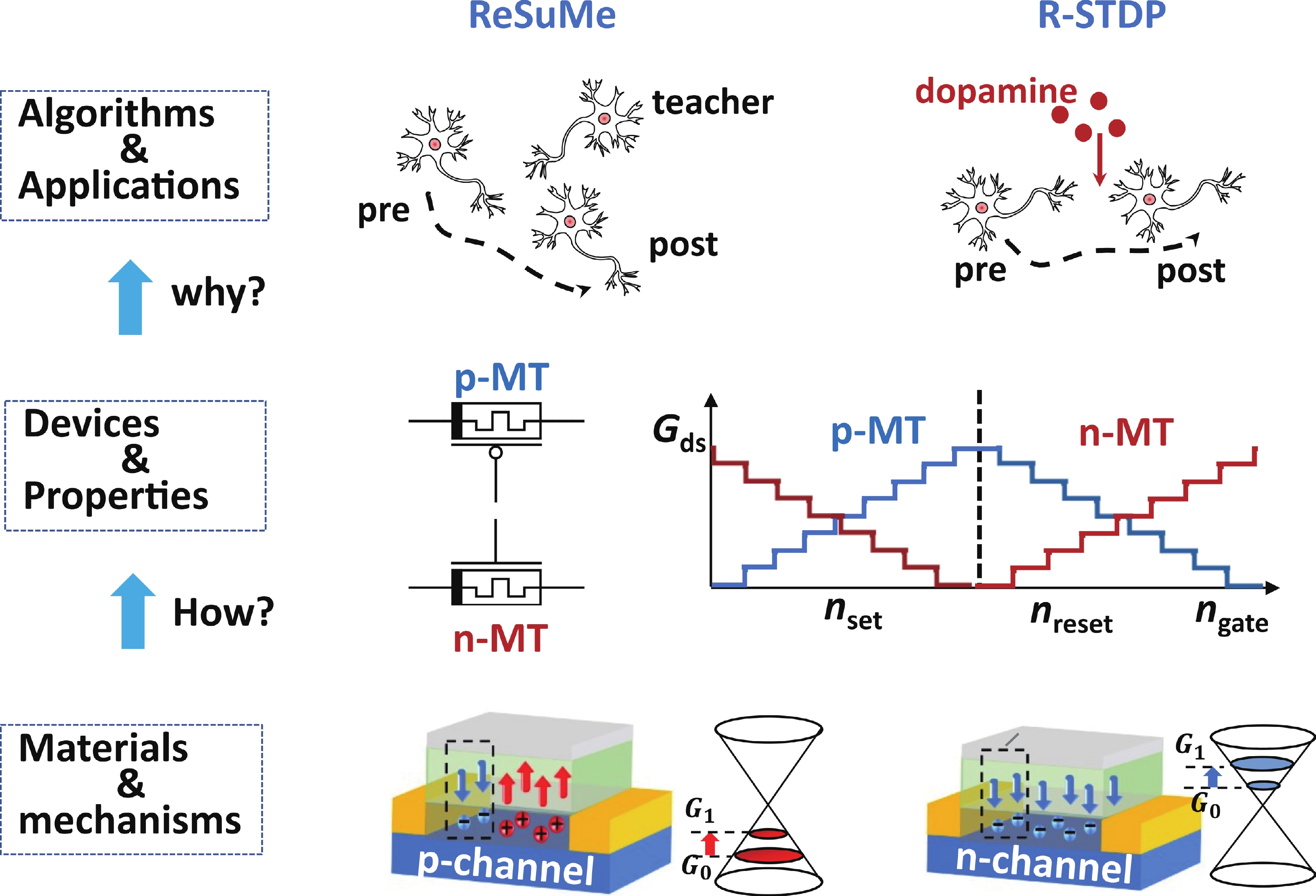
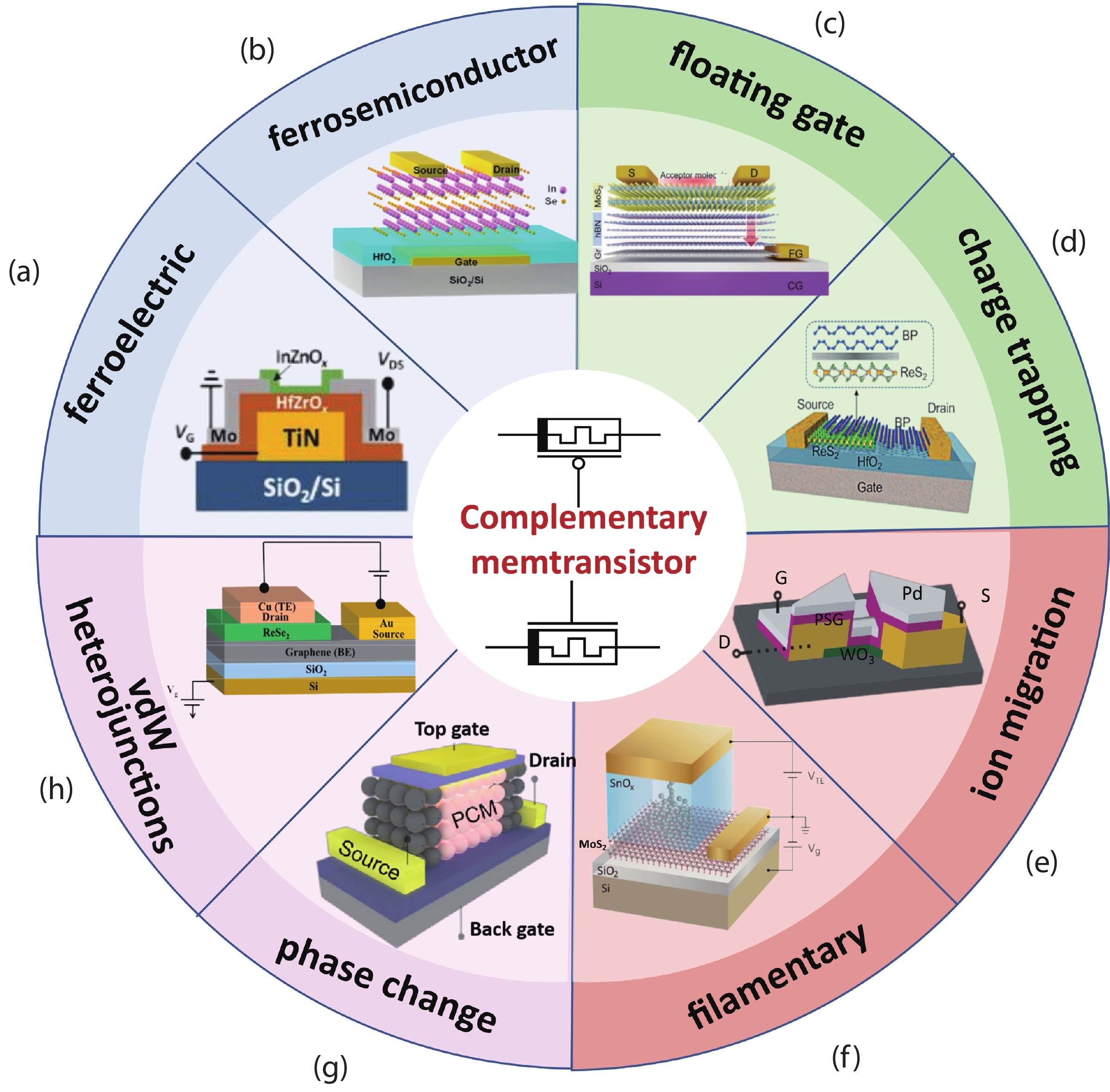
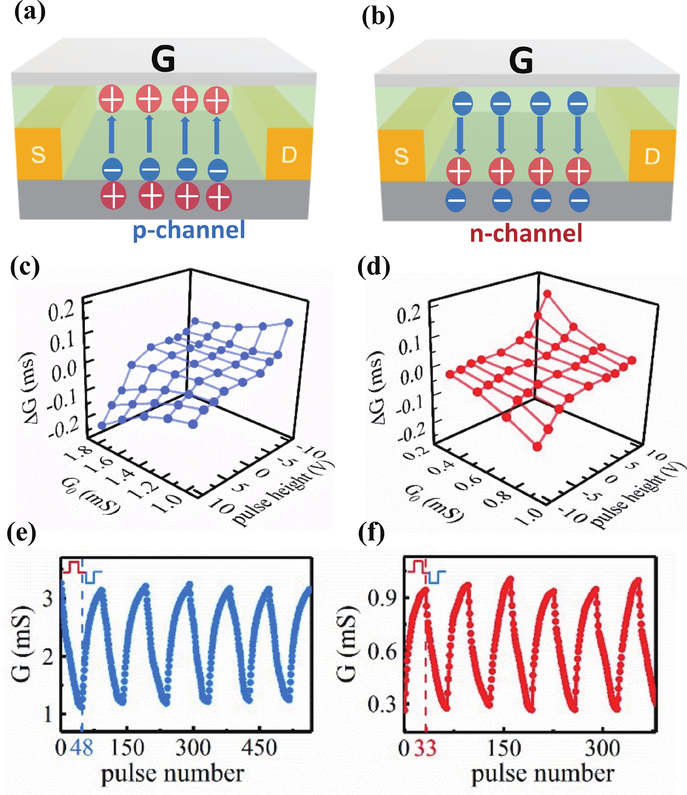
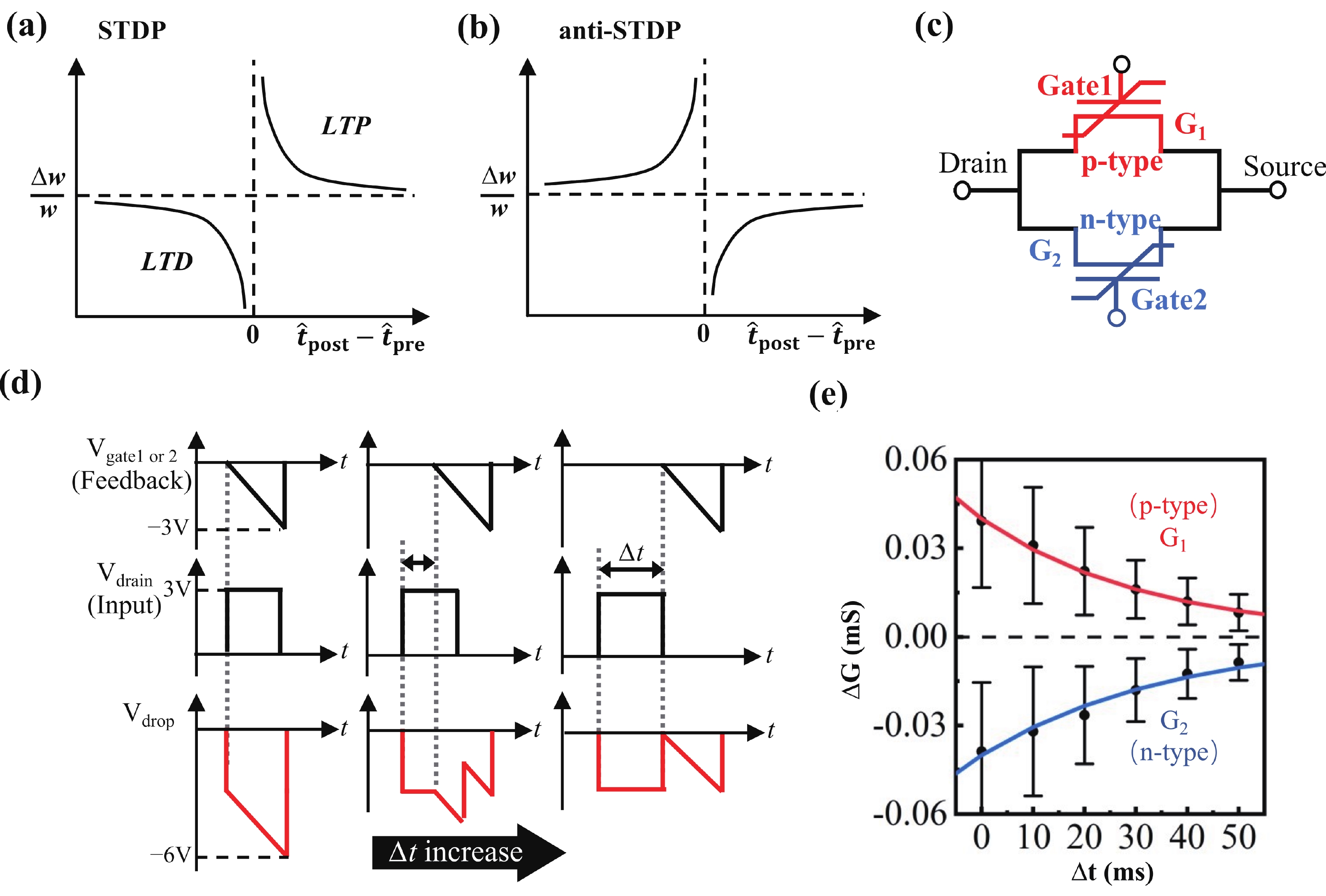
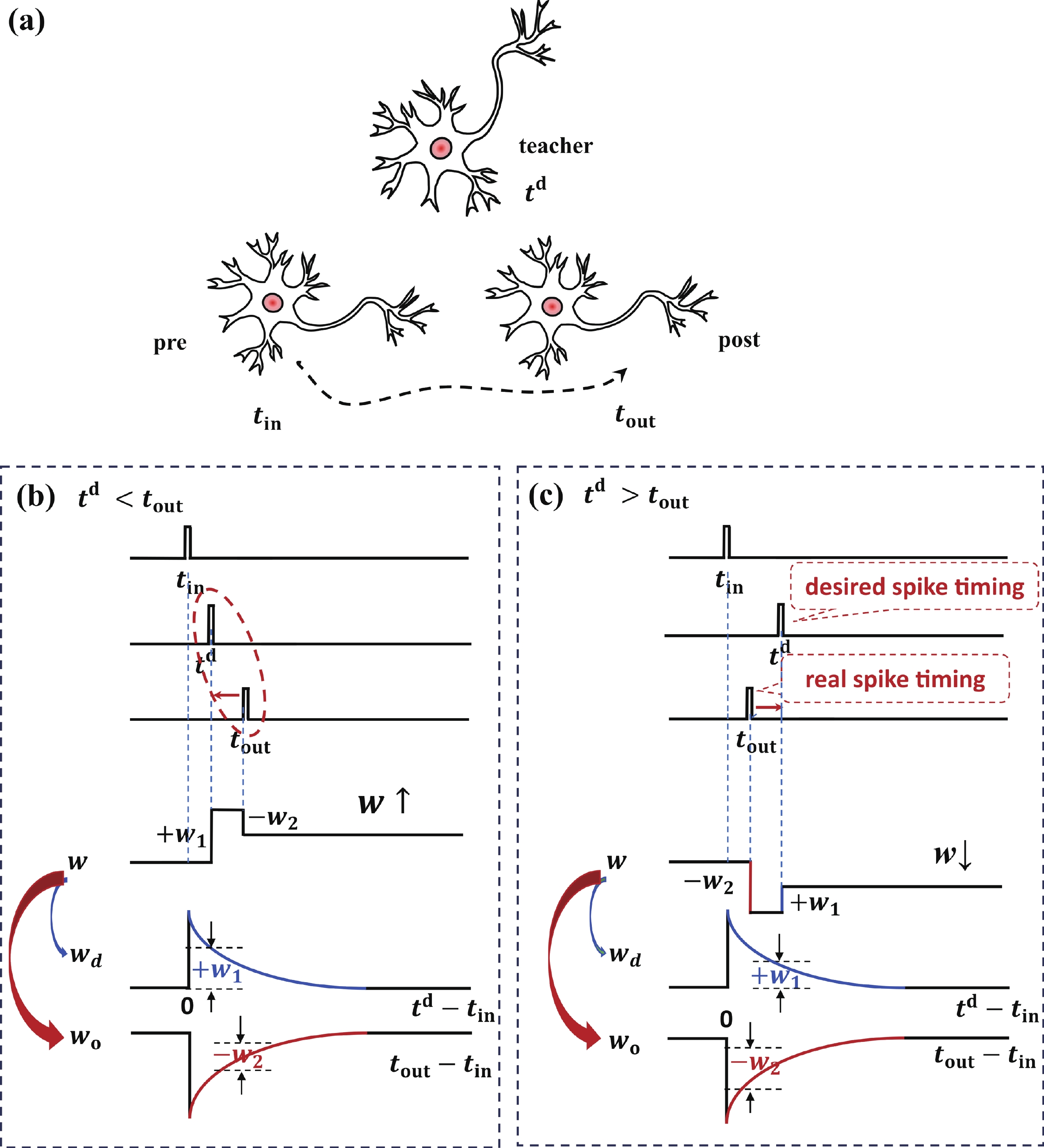
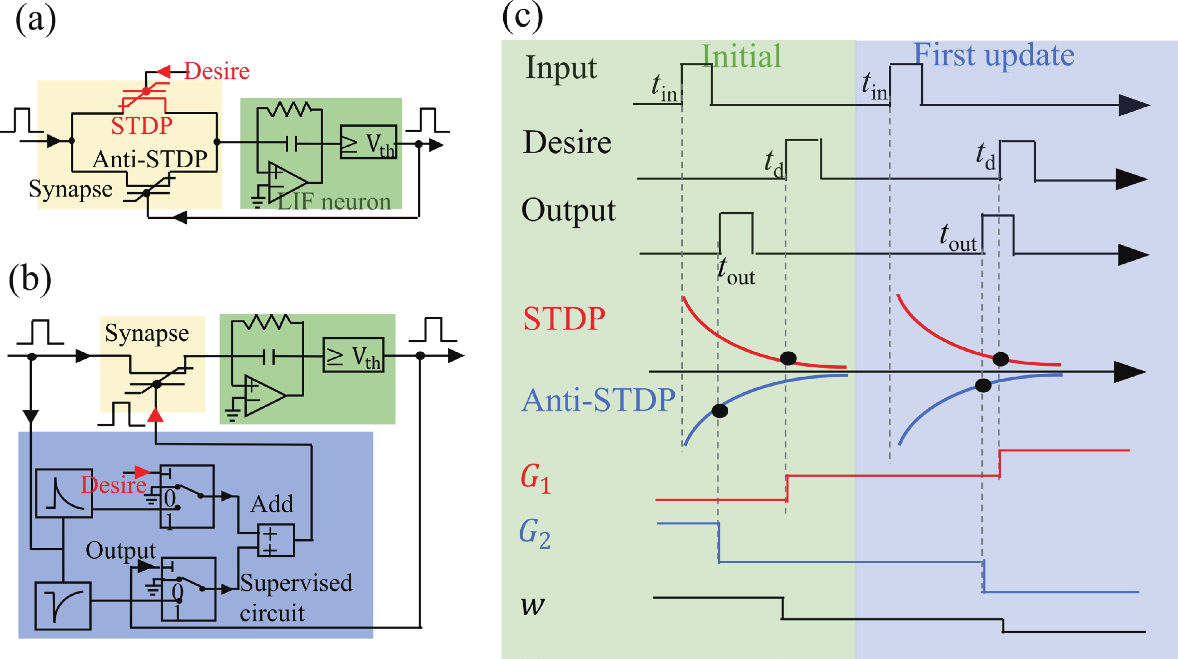
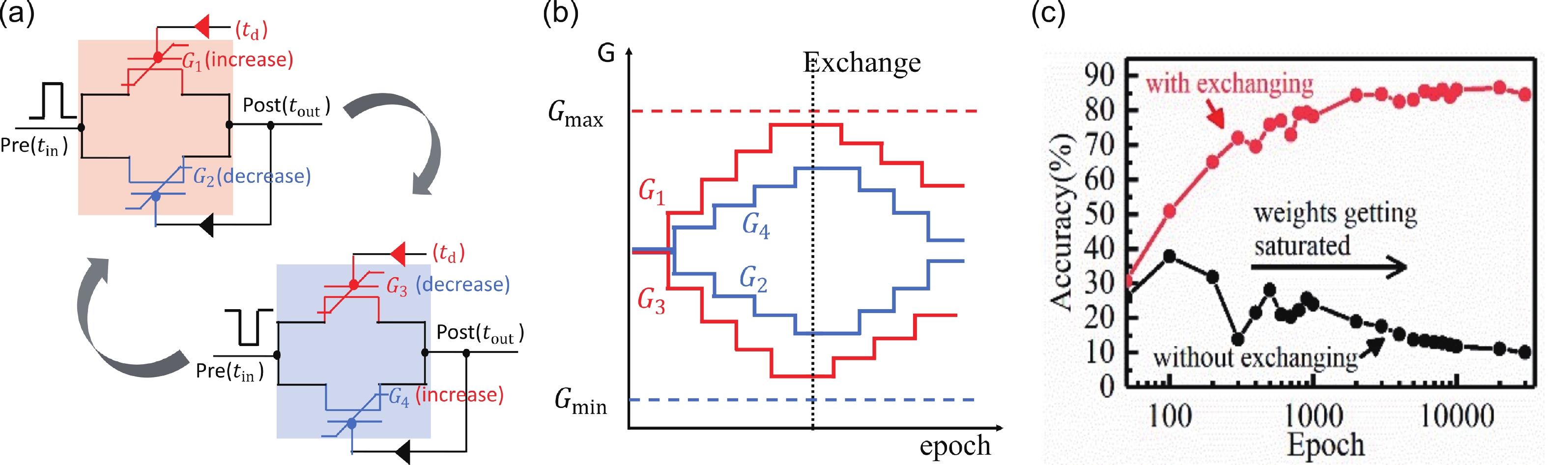
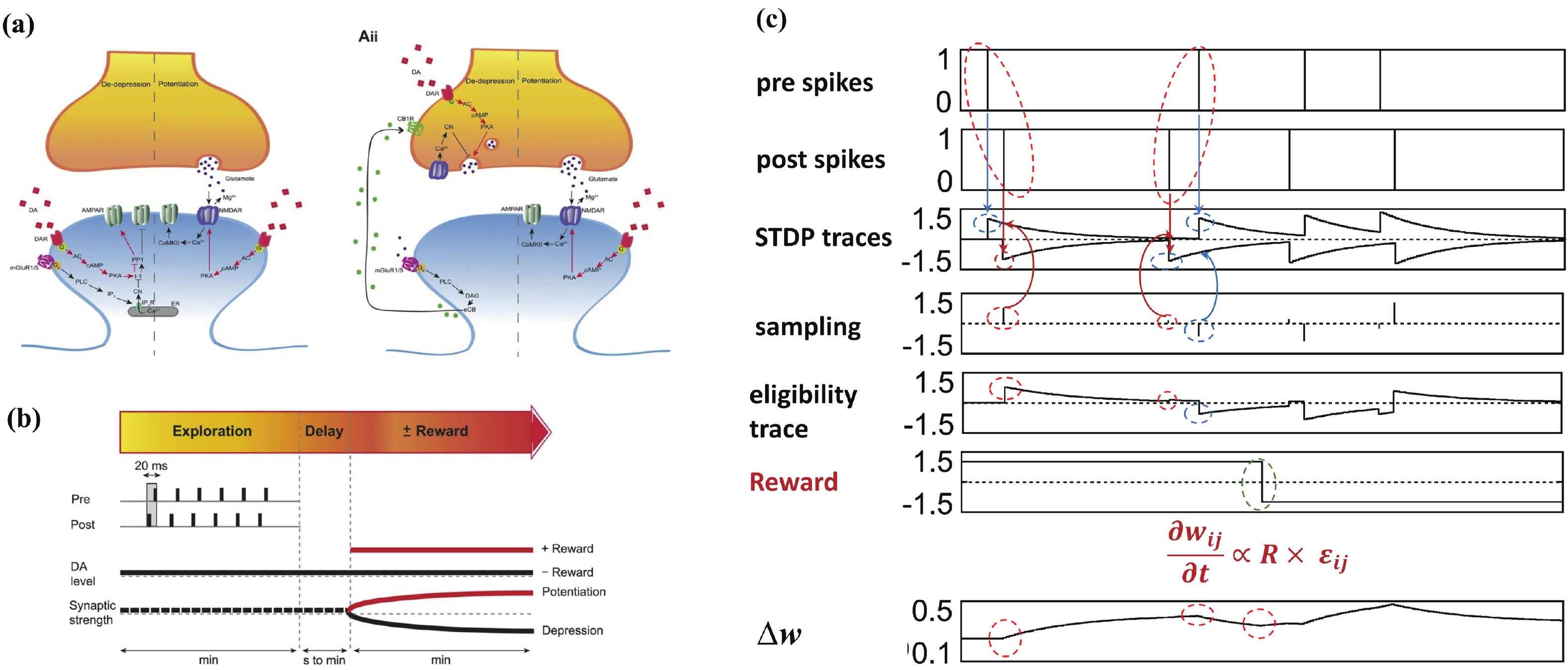
Table 1. Mechanisms for nonvolatile conductance tuning in memtransistors and the key indices of performance of them.
| Mechanism | Channel layer |
Memory layer |
Operating voltage (V) |
On/off ratio |
Endurance (cycles) |
Retention (s) |
Speed (s) |
Ref | |
| Ferroelectric | InZnOx | HfZrOx | <5 | ~104 | >108 | N/A | <10-6 | [13] | |
| Ferrosemi-conductor | InSe | 4 | >106 | >100 | >104 | 2 × 10⁻⁷ | [14] | ||
| Charge trapping | BP-ReS2 | POx | 4 | 106 | N/A | 50 | 10−3 | [16] | |
| Floating gate | MoS2 | Gr | 6 | >105 | 30 | N/A | 10−4 | [15] | |
| Ion migration | WO3 | 8.5/10 | 20 | >105 | ~102 | N/A | [17] | ||
| Filamentary | MoS2&SnOx | 5 | ~108 | 106 | N/A | N/A | [18] | ||
| Phase change | Ge15Sb85&Sb | N/A | 102 | 1015 | N/A | N/A | [19] | ||
| vdW hetero-junctions | ReSe2&graphene | N/A | 103 | 103 | ~104 | N/A | [20] | ||
 DownLoad: CSV
| [1] |
Chua L. Memristor-The missing circuit element. IEEE Transactions on Circuit Theory, 1971, 18(5), 507 doi: 10.1109/TCT.1971.1083337
|
| [2] |
Strukov D B, Snider G S, Stewart D R, et al. The missing memristor found. Nature, 2008, 453(7191), 80 doi: 10.1038/nature06932
|
| [3] |
Jo S H, Chang T, Ebong I, et al. Nanoscale memristor device as synapse in neuromorphic systems. Nano Lett, 2010, 10(4), 1297 doi: 10.1021/nl904092h
|
| [4] |
Alibart F, Zamanidoost E, Strukov D B. Pattern classification by memristive crossbar circuits using ex situ and in situ training. Nat Commun, 2013, 4, 2072 doi: 10.1038/ncomms3072
|
| [5] |
Yao P, Wu H, Gao B, et al. Face classification using electronic synapses. Nat Commun, 2017, 8, 15199 doi: 10.1038/ncomms15199
|
| [6] |
Wang Z R, Joshi S, Savel’ev S, et al. Fully memristive neural networks for pattern classification with unsupervised learning. Nat Electron, 2018, 1(2), 137 doi: 10.1038/s41928-018-0023-2
|
| [7] |
Cai F X, Correll J M, Lee S H, et al. A fully integrated reprogrammable memristor–CMOS system for efficient multiply–accumulate operations. Nat Electron, 2019, 2(7), 290 doi: 10.1038/s41928-019-0270-x
|
| [8] |
Yao P, Wu H Q, Gao B, et al. Fully hardware-implemented memristor convolutional neural network. Nature, 2020, 577(7792), 641 doi: 10.1038/s41586-020-1942-4
|
| [9] |
Sangwan V K, Lee H S, Bergeron H, et al. Multi-terminal memtransistors from polycrystalline monolayer molybdenum disulfide. Nature, 2018, 554(7693), 500 doi: 10.1038/nature25747
|
| [10] |
Yan X D, Qian J H, Sangwan V K, et al. Progress and challenges for memtransistors in neuromorphic circuits and systems. Adv Mater, 2022, 34(48), e2108025 doi: 10.1002/adma.202108025
|
| [11] |
Nishitani Y, Kaneko Y, Ueda M. Supervised learning using spike-timing-dependent plasticity of memristive synapses. IEEE Trans Neural Netw Learn Syst, 2015, 26(12), 2999 doi: 10.1109/TNNLS.2015.2399491
|
| [12] |
Chen Y Y, Zhou Y, Zhuge F W, et al. Graphene–ferroelectric transistors as complementary synapses for supervised learning in spiking neural network. NPJ 2D Mater Appl, 2019, 3(1), 31 doi: 10.1038/s41699-019-0114-6
|
| [13] |
Kim M K, Kim I J, Lee J S. CMOS-compatible ferroelectric NAND flash memory for high-density, low-power, and high-speed three-dimensional memory. Sci Adv, 2021, 7(3), eabe1341 doi: 10.1126/sciadv.abe1341
|
| [14] |
Liao J Y, Wen W, Wu J X, et al. Van der waals ferroelectric semiconductor field effect transistor for in-memory computing. ACS Nano, 2023, 17(6), 6095 doi: 10.1021/acsnano.3c01198
|
| [15] |
Wang H, Lu Y L, Liu S B, et al. Adaptive neural activation and neuromorphic processing via drain-injection threshold-switching float gate transistor memory. Adv Mater, 2023, 35, 2309099 doi: 10.1002/adma.202309099
|
| [16] |
Xiong X, Kang J Y, Hu Q L, et al. Reconfigurable logic-in-memory and multilingual artificial synapses based on 2D heterostructures. Adv Funct Materials, 2020, 30(11), 1909645 doi: 10.1002/adfm.201909645
|
| [17] |
Onen M, Emond N, Wang B M, et al. Nanosecond protonic programmable resistors for analog deep learning. Science, 2022, 377(6605), 539 doi: 10.1126/science.abp8064
|
| [18] |
Yan X D, Ma J H, Wu T, et al. Reconfigurable Stochastic neurons based on tin oxide/MoS2 hetero-memristors for simulated annealing and the Boltzmann machine. Nat Commun, 2021, 12(1), 5710 doi: 10.1038/s41467-021-26012-5
|
| [19] |
Sarwat S G, Kersting B, Moraitis T, et al. Phase-change memtransistive synapses for mixed-plasticity neural computations. Nat Nanotechnol, 2022, 17(5), 507 doi: 10.1038/s41565-022-01095-3
|
| [20] |
Shania R, Honggyun K, Farooq K M, et al. Tunable resistive switching of vertical ReSe2/graphene hetero-structure enabled by Schottky barrier height and DUV light. J Alloys Compd, 2021, 855, 157310 doi: 10.1016/j.jallcom.2020.157310
|
| [21] |
Ali T, Polakowski P, Riedel S, et al. High endurance ferroelectric hafnium oxide-based FeFET memory without retention penalty. IEEE Trans Electron Devices, 2018, 65(9), 3769 doi: 10.1109/TED.2018.2856818
|
| [22] |
Dünkel S, Trentzsch M, Richter R, et al. A FeFET based super-low-power ultra-fast embedded NVM technology for 22nm FDSOI and beyond. 2017 IEEE International Electron Devices Meeting (IEDM). San Francisco, CA, USA. IEEE, 2017, 19.7. 1 doi: 10.1109/IEDM.2017.8268425
|
| [23] |
Tanaka H, Kido M, Yahashi K, et al. Bit cost scalable technology with punch and plug process for ultra high density flash memory. 2007 IEEE Symposium on VLSI Technology. Kyoto, Japan. IEEE, 2007, 14 doi: 10.1109/VLSIT.2007.4339708
|
| [24] |
Kim K H, Song S, Kim B, et al. Tuning polarity in WSe2/AlScN FeFETs via contact engineering. ACS Nano, 2024, 18(5), 4180 doi: 10.1021/acsnano.3c09279
|
| [25] |
Chou Y C, Tsai C W, Yi C Y, et al. Neuro-inspired-in-memory computing using charge-trapping MemTransistor on germanium as synaptic device. IEEE Trans Electron Devices, 2020, 67(9), 3605 doi: 10.1109/TED.2020.3008887
|
| [26] |
Yao X H, Klyukin K, Lu W J, et al. Protonic solid-state electrochemical synapse for physical neural networks. Nat Commun, 2020, 11(1), 3134 doi: 10.1038/s41467-020-16866-6
|
| [27] |
Nikam R D, Kwak M, Hwang H. All-solid-state oxygen ion electrochemical random-access memory for neuromorphic computing. Adv Elect Materials, 2021, 7(5), 2100142 doi: 10.1002/aelm.202100142
|
| [28] |
Fuller E J, Gabaly F E, Léonard F, et al. Li-ion synaptic transistor for low power analog computing. Adv Mater, 2017, 29, 1604310 doi: 10.1002/adma.201604310
|
| [29] |
Song M K, Kang J H, Zhang X, et al. Recent advances and future prospects for memristive materials, devices, and systems. ACS Nano, 2023, 17(3), 11994 doi: 10.1021/acsnano.3c03505
|
| [30] |
Onen M, Emond N, Li J, et al. CMOS-compatible protonic programmable resistor based on phosphosilicate glass electrolyte for analog deep learning. Nano Lett, 2021, 21(14), 6111 doi: 10.1021/acs.nanolett.1c01614
|
| [31] |
Qian C, Kong L A, Yang J L, et al. Multi-gate organic neuron transistors for spatiotemporal information processing. Appl Phys Lett, 2017, 110(8), 083302 doi: 10.1063/1.4977069
|
| [32] |
Yang Y, Du H Y, Xue Q, et al. Three-terminal memtransistors based on two-dimensional layered gallium selenide nanosheets for potential low-power electronics applications. Nano Energy, 2018, 57, 566 doi: 10.1016/j.nanoen.2018.12.057
|
| [33] |
Iqbal S, Duy L T, Kang H, et al. Femtojoule-power-consuming synaptic memtransistor based on Mott transition of multiphasic vanadium oxides. Adv Funct Materials, 2021, 31(46), 2102567 doi: 10.1002/adfm.202102567
|
| [34] |
Zhou Y, Xu N, Gao B, et al. Complementary graphene-ferroelectric transistors (C-GFTs) as synapses with modulatable plasticity for supervised learning. 2019 IEEE International Electron Devices Meeting (IEDM). San Francisco, CA, USA. IEEE, 2019, 6.5. 1 doi: 10.1109/IEDM19573.2019.8993453
|
| [35] |
Markram H, Lübke J, Frotscher M, et al. Regulation of synaptic efficacy by coincidence of postsynaptic APs and EPSPs. Science, 1997, 275(5297), 213 doi: 10.1126/science.275.5297.213
|
| [36] |
Bi G Q, Poo M M. Synaptic modifications in cultured hippocampal neurons: Dependence on spike timing, synaptic strength, and postsynaptic cell type. J Neurosci, 1998, 18(24), 10464 doi: 10.1523/JNEUROSCI.18-24-10464.1998
|
| [37] |
Yuan J T, Liu S E, Shylendra A, et al. Reconfigurable MoS2 memtransistors for continuous learning in spiking neural networks. Nano Lett, 2021, 21(15), 6432 doi: 10.1021/acs.nanolett.1c00982
|
| [38] |
Nishitani Y, Kaneko Y, Ueda M, et al. Three-terminal ferroelectric synapse device with concurrent learning function for artificial neural networks. J Appl Phys, 2012, 111(12), 124108 doi: 10.1063/1.4729915
|
| [39] |
Zhai Y B, Xie P, Feng Z H, et al. 2D heterostructure for high-order spatiotemporal information processing. Adv Funct Materials, 2022, 32(7), 2108440 doi: 10.1002/adfm.202108440
|
| [40] |
Wang L, Liao W G, Wong S L, et al. Artificial synapses based on multiterminal memtransistors for neuromorphic application. Adv Funct Materials, 2019, 29(25), 1901106 doi: 10.1002/adfm.201901106
|
| [41] |
Leong J F, Fang Z H, Sivan M, et al. N-P reconfigurable dual-mode memtransistors for compact bio-inspired feature extractor with inhibitory-excitatory spiking capability. Adv Funct Materials, 2023, 33(45), 2302949 doi: 10.1002/adfm.202302949
|
| [42] |
Zhou Y, Xu N, Gao B, et al. Complementary memtransistor-based multilayer neural networks for online supervised learning through (anti-) spike-timing-dependent plasticity. IEEE Trans Neural Netw Learn Syst, 2022, 33(11), 6640 doi: 10.1109/TNNLS.2021.3082911
|
| [43] |
Shouval H Z, Wang S S H, Wittenberg G M. Spike timing dependent plasticity: A consequence of more fundamental learning rules. Front Comput Neurosci, 2010, 4, 19 doi: 10.3389/fncom.2010.00019
|
| [44] |
Ponulak F, Kasiński A. Supervised learning in spiking neural networks with ReSuMe: Sequence learning, classification, and spike shifting. Neural Comput, 2010, 22(2), 467 doi: 10.1162/neco.2009.11-08-901
|
| [45] |
Sporea I, Grüning A. Supervised learning in multilayer spiking neural networks. Neural Comput, 2013, 25(2), 473 doi: 10.1162/NECO_a_00396
|
| [46] |
Jerry M, Chen P Y, Zhang J C, et al. Ferroelectric FET analog synapse for acceleration of deep neural network training. 2017 IEEE International Electron Devices Meeting (IEDM), 2017, 6.2. 1 doi: 10.1109/IEDM.2017.8268338
|
| [47] |
Seo M, Kang M H, Jeon S B, et al. First demonstration of a logic-process compatible junctionless ferroelectric FinFET synapse for neuromorphic applications. IEEE Electron Device Lett, 2018, 39, 1445 doi: 10.1109/LED.2018.2852698
|
| [48] |
Woo J, Moon K, Song J, et al. Improved synaptic behavior under identical pulses using AlO x/HfO2 bilayer RRAM array for neuromorphic systems. IEEE Electron Device Lett, 2016, 37, 994 doi: 10.1109/LED.2016.2582859
|
| [49] |
Brzosko Z, Schultz W, Paulsen O. Retroactive modulation of spike timing-dependent plasticity by dopamine. eLife, 2015, 4, e09685 doi: 10.7554/eLife.09685
|
| [50] |
Florian R V. Reinforcement learning through modulation of spike-timing-dependent synaptic plasticity. Neural Comput, 2007, 19(6), 1468 doi: 10.1162/neco.2007.19.6.1468
|
| [51] |
Zhou Y, Wang Y S, Zhuge F W, et al. A reconfigurable two-WSe2-transistor synaptic cell for reinforcement learning. Adv Mater, 2022, 34(48), e2107754 doi: 10.1002/adma.202107754
|
| [52] |
Shi C, Lu J, Wang Y, et al. Exploiting memristors for neuromorphic reinforcement learning. 2021 IEEE 3rd International Conference on Artificial Intelligence Circuits and Systems (AICAS), 2021, 1 doi: 10.1109/AICAS51828.2021.9458542
|
| [53] |
Gerstner W, Kistler W M, Naud R, et al. Neuronal dynamics: From single neurons to networks and models of cognition. New York, NY: Cambridge University Press
|
| [54] |
Oh S, Hwang H, Yoo I K. Ferroelectric materials for neuromorphic computing. APL Mater, 2019, 7(9), 091109 doi: 10.1063/1.5108562
|
| [55] |
Chang T, Jo S H, Lu W. Short-term memory to long-term memory transition in a nanoscale memristor. ACS Nano, 2011, 5(9), 7669 doi: 10.1021/nn202983n
|
| [56] |
Zhou Y, Fu J W, Chen Z R, et al. Computational event-driven vision sensors for in-sensor spiking neural networks. Nat Electron, 2023, 6(11), 870 doi: 10.1038/s41928-023-01055-2
|
| [57] |
Zhou Y, Fu J W, Wan T Q, et al. A 2T2R1C vision cell with 140 dB dynamic range and event-driven characteristics for in-sensor spiking neural network. 2022 International Electron Devices Meeting (IEDM). San Francisco, CA, USA. IEEE, 2022, 31.4. 1 doi: 10.1109/IEDM45625.2022.10019350
|
| [58] |
Zhou F C, Chai Y. Near-sensor and in-sensor computing. Nat Electron, 2020, 3(11), 664 doi: 10.1038/s41928-020-00501-9
|
| [59] |
Mennel L, Symonowicz J, Wachter S, et al. Ultrafast machine vision with 2D material neural network image sensors. Nature, 2020, 579(7797), 62 doi: 10.1038/s41586-020-2038-x
|
| [60] |
Wan T Q, Shao B J, Ma S J, et al. In-sensor computing: Materials, devices, and integration technologies. Adv Mater, 2023, 35(37), e2203830 doi: 10.1002/adma.202203830
|
| [61] |
Yang Y K, Pan C, Li Y X, et al. In-sensor dynamic computing for intelligent machine vision. Nat Electron, 2024 doi: 10.1038/s41928-024-01124-0
|
| [62] |
Bichler O, Querlioz D, Thorpe S J, et al. Extraction of temporally correlated features from dynamic vision sensors with spike-timing-dependent plasticity. Neural Netw, 2012, 32, 339 doi: 10.1016/j.neunet.2012.02.022
|
| [63] |
Bichler O, Suri M, Querlioz D, et al. Visual pattern extraction using energy-efficient "2-PCM synapse" neuromorphic architecture. IEEE Trans Electron Devices, 2012, 59(8), 2206 doi: 10.1109/TED.2012.2197951
|
| [64] |
Kim Y, Panda P. Optimizing deeper spiking neural networks for dynamic vision sensing. Neural Netw, 2021, 144, 686 doi: 10.1016/j.neunet.2021.09.022
|
| [65] |
Stromatias E, Soto M, Serrano-Gotarredona T, et al. An event-driven classifier for spiking neural networks fed with synthetic or dynamic vision sensor data. Front Neurosci, 2017, 11, 350 doi: 10.3389/fnins.2017.00350
|
| [66] |
Tsai M Y, Huang C T, Lin C Y, et al. A reconfigurable transistor and memory based on a two-dimensional heterostructure and photoinduced trapping. Nat Electron, 2023, 6(10), 755 doi: 10.1038/s41928-023-01034-7
|
| [67] |
Fang W, Chen Y Q, Ding J H, et al. SpikingJelly: An open-source machine learning infrastructure platform for spike-based intelligence. Sci Adv, 2023, 9(40), eadi1480 doi: 10.1126/sciadv.adi1480
|
| [68] |
Mozafari M, Ganjtabesh M, Nowzari-Dalini A, et al. Bio-inspired digit recognition using reward-modulated spike-timing-dependent plasticity in deep convolutional networks. Pattern Recognit, 2019, 94, 87 doi: 10.1016/j.patcog.2019.05.015
|


Article views: 3144 Times PDF downloads: 291 Times Cited by: 0 Times
Received: 28 December 2023 Revised: 17 February 2024 Online: Accepted Manuscript: 06 March 2024Uncorrected proof: 08 March 2024Published: 15 June 2024
| Citation: |
Qi Chen, Yue Zhou, Weiwei Xiong, Zirui Chen, Yasai Wang, Xiangshui Miao, Yuhui He. Complementary memtransistors for neuromorphic computing: How, what and why[J]. Journal of Semiconductors, 2024, 45(6): 061701. doi: 10.1088/1674-4926/23120051
****
Q Chen, Y Zhou, W W Xiong, Z R Chen, Y S Wang, X S Miao, and Y H He, Complementary memtransistors for neuromorphic computing: How, what and why[J]. J. Semicond., 2024, 45(6), 061701 doi: 10.1088/1674-4926/23120051

|
 Qi Chen got her Bachelor and Master’s degrees in 2009 and 2011 from School of Electrical Engineering, Wuhan University. Now she is an engineer at School of Integrated Circuits, Huazhong University of Science and Technology, responsible for teaching and experiments on microelectronics
 Yue Zhou got her Bachelor’s and Ph.D in 2018 and 2023 from School of Integrated Circuits, Huazhong University of Science and Technology. During Ph.D study, she published several first-author papers on Nature Electronics, International Electronic Device Meeting (IEDM), and received the 1st class Scholarship on Integrated Circuits by Chinese Institute of Electronics. She is now a post-doc at University of California, San Diego, USA
 Yuhui He got his Bachelor’s and Ph.D in 2003 and 2009 from Department of Microelectronics, Peking University. He is now a professor at School of Integrated Circuits, Huazhong University of Science and Technology. His research focuses on nanoelectronic devices and circuits for neuromorphic computing
| [1] |
Chua L. Memristor-The missing circuit element. IEEE Transactions on Circuit Theory, 1971, 18(5), 507 doi: 10.1109/TCT.1971.1083337
|
| [2] |
Strukov D B, Snider G S, Stewart D R, et al. The missing memristor found. Nature, 2008, 453(7191), 80 doi: 10.1038/nature06932
|
| [3] |
Jo S H, Chang T, Ebong I, et al. Nanoscale memristor device as synapse in neuromorphic systems. Nano Lett, 2010, 10(4), 1297 doi: 10.1021/nl904092h
|
| [4] |
Alibart F, Zamanidoost E, Strukov D B. Pattern classification by memristive crossbar circuits using ex situ and in situ training. Nat Commun, 2013, 4, 2072 doi: 10.1038/ncomms3072
|
| [5] |
Yao P, Wu H, Gao B, et al. Face classification using electronic synapses. Nat Commun, 2017, 8, 15199 doi: 10.1038/ncomms15199
|
| [6] |
Wang Z R, Joshi S, Savel’ev S, et al. Fully memristive neural networks for pattern classification with unsupervised learning. Nat Electron, 2018, 1(2), 137 doi: 10.1038/s41928-018-0023-2
|
| [7] |
Cai F X, Correll J M, Lee S H, et al. A fully integrated reprogrammable memristor–CMOS system for efficient multiply–accumulate operations. Nat Electron, 2019, 2(7), 290 doi: 10.1038/s41928-019-0270-x
|
| [8] |
Yao P, Wu H Q, Gao B, et al. Fully hardware-implemented memristor convolutional neural network. Nature, 2020, 577(7792), 641 doi: 10.1038/s41586-020-1942-4
|
| [9] |
Sangwan V K, Lee H S, Bergeron H, et al. Multi-terminal memtransistors from polycrystalline monolayer molybdenum disulfide. Nature, 2018, 554(7693), 500 doi: 10.1038/nature25747
|
| [10] |
Yan X D, Qian J H, Sangwan V K, et al. Progress and challenges for memtransistors in neuromorphic circuits and systems. Adv Mater, 2022, 34(48), e2108025 doi: 10.1002/adma.202108025
|
| [11] |
Nishitani Y, Kaneko Y, Ueda M. Supervised learning using spike-timing-dependent plasticity of memristive synapses. IEEE Trans Neural Netw Learn Syst, 2015, 26(12), 2999 doi: 10.1109/TNNLS.2015.2399491
|
| [12] |
Chen Y Y, Zhou Y, Zhuge F W, et al. Graphene–ferroelectric transistors as complementary synapses for supervised learning in spiking neural network. NPJ 2D Mater Appl, 2019, 3(1), 31 doi: 10.1038/s41699-019-0114-6
|
| [13] |
Kim M K, Kim I J, Lee J S. CMOS-compatible ferroelectric NAND flash memory for high-density, low-power, and high-speed three-dimensional memory. Sci Adv, 2021, 7(3), eabe1341 doi: 10.1126/sciadv.abe1341
|
| [14] |
Liao J Y, Wen W, Wu J X, et al. Van der waals ferroelectric semiconductor field effect transistor for in-memory computing. ACS Nano, 2023, 17(6), 6095 doi: 10.1021/acsnano.3c01198
|
| [15] |
Wang H, Lu Y L, Liu S B, et al. Adaptive neural activation and neuromorphic processing via drain-injection threshold-switching float gate transistor memory. Adv Mater, 2023, 35, 2309099 doi: 10.1002/adma.202309099
|
| [16] |
Xiong X, Kang J Y, Hu Q L, et al. Reconfigurable logic-in-memory and multilingual artificial synapses based on 2D heterostructures. Adv Funct Materials, 2020, 30(11), 1909645 doi: 10.1002/adfm.201909645
|
| [17] |
Onen M, Emond N, Wang B M, et al. Nanosecond protonic programmable resistors for analog deep learning. Science, 2022, 377(6605), 539 doi: 10.1126/science.abp8064
|
| [18] |
Yan X D, Ma J H, Wu T, et al. Reconfigurable Stochastic neurons based on tin oxide/MoS2 hetero-memristors for simulated annealing and the Boltzmann machine. Nat Commun, 2021, 12(1), 5710 doi: 10.1038/s41467-021-26012-5
|
| [19] |
Sarwat S G, Kersting B, Moraitis T, et al. Phase-change memtransistive synapses for mixed-plasticity neural computations. Nat Nanotechnol, 2022, 17(5), 507 doi: 10.1038/s41565-022-01095-3
|
| [20] |
Shania R, Honggyun K, Farooq K M, et al. Tunable resistive switching of vertical ReSe2/graphene hetero-structure enabled by Schottky barrier height and DUV light. J Alloys Compd, 2021, 855, 157310 doi: 10.1016/j.jallcom.2020.157310
|
| [21] |
Ali T, Polakowski P, Riedel S, et al. High endurance ferroelectric hafnium oxide-based FeFET memory without retention penalty. IEEE Trans Electron Devices, 2018, 65(9), 3769 doi: 10.1109/TED.2018.2856818
|
| [22] |
Dünkel S, Trentzsch M, Richter R, et al. A FeFET based super-low-power ultra-fast embedded NVM technology for 22nm FDSOI and beyond. 2017 IEEE International Electron Devices Meeting (IEDM). San Francisco, CA, USA. IEEE, 2017, 19.7. 1 doi: 10.1109/IEDM.2017.8268425
|
| [23] |
Tanaka H, Kido M, Yahashi K, et al. Bit cost scalable technology with punch and plug process for ultra high density flash memory. 2007 IEEE Symposium on VLSI Technology. Kyoto, Japan. IEEE, 2007, 14 doi: 10.1109/VLSIT.2007.4339708
|
| [24] |
Kim K H, Song S, Kim B, et al. Tuning polarity in WSe2/AlScN FeFETs via contact engineering. ACS Nano, 2024, 18(5), 4180 doi: 10.1021/acsnano.3c09279
|
| [25] |
Chou Y C, Tsai C W, Yi C Y, et al. Neuro-inspired-in-memory computing using charge-trapping MemTransistor on germanium as synaptic device. IEEE Trans Electron Devices, 2020, 67(9), 3605 doi: 10.1109/TED.2020.3008887
|
| [26] |
Yao X H, Klyukin K, Lu W J, et al. Protonic solid-state electrochemical synapse for physical neural networks. Nat Commun, 2020, 11(1), 3134 doi: 10.1038/s41467-020-16866-6
|
| [27] |
Nikam R D, Kwak M, Hwang H. All-solid-state oxygen ion electrochemical random-access memory for neuromorphic computing. Adv Elect Materials, 2021, 7(5), 2100142 doi: 10.1002/aelm.202100142
|
| [28] |
Fuller E J, Gabaly F E, Léonard F, et al. Li-ion synaptic transistor for low power analog computing. Adv Mater, 2017, 29, 1604310 doi: 10.1002/adma.201604310
|
| [29] |
Song M K, Kang J H, Zhang X, et al. Recent advances and future prospects for memristive materials, devices, and systems. ACS Nano, 2023, 17(3), 11994 doi: 10.1021/acsnano.3c03505
|
| [30] |
Onen M, Emond N, Li J, et al. CMOS-compatible protonic programmable resistor based on phosphosilicate glass electrolyte for analog deep learning. Nano Lett, 2021, 21(14), 6111 doi: 10.1021/acs.nanolett.1c01614
|
| [31] |
Qian C, Kong L A, Yang J L, et al. Multi-gate organic neuron transistors for spatiotemporal information processing. Appl Phys Lett, 2017, 110(8), 083302 doi: 10.1063/1.4977069
|
| [32] |
Yang Y, Du H Y, Xue Q, et al. Three-terminal memtransistors based on two-dimensional layered gallium selenide nanosheets for potential low-power electronics applications. Nano Energy, 2018, 57, 566 doi: 10.1016/j.nanoen.2018.12.057
|
| [33] |
Iqbal S, Duy L T, Kang H, et al. Femtojoule-power-consuming synaptic memtransistor based on Mott transition of multiphasic vanadium oxides. Adv Funct Materials, 2021, 31(46), 2102567 doi: 10.1002/adfm.202102567
|
| [34] |
Zhou Y, Xu N, Gao B, et al. Complementary graphene-ferroelectric transistors (C-GFTs) as synapses with modulatable plasticity for supervised learning. 2019 IEEE International Electron Devices Meeting (IEDM). San Francisco, CA, USA. IEEE, 2019, 6.5. 1 doi: 10.1109/IEDM19573.2019.8993453
|
| [35] |
Markram H, Lübke J, Frotscher M, et al. Regulation of synaptic efficacy by coincidence of postsynaptic APs and EPSPs. Science, 1997, 275(5297), 213 doi: 10.1126/science.275.5297.213
|
| [36] |
Bi G Q, Poo M M. Synaptic modifications in cultured hippocampal neurons: Dependence on spike timing, synaptic strength, and postsynaptic cell type. J Neurosci, 1998, 18(24), 10464 doi: 10.1523/JNEUROSCI.18-24-10464.1998
|
| [37] |
Yuan J T, Liu S E, Shylendra A, et al. Reconfigurable MoS2 memtransistors for continuous learning in spiking neural networks. Nano Lett, 2021, 21(15), 6432 doi: 10.1021/acs.nanolett.1c00982
|
| [38] |
Nishitani Y, Kaneko Y, Ueda M, et al. Three-terminal ferroelectric synapse device with concurrent learning function for artificial neural networks. J Appl Phys, 2012, 111(12), 124108 doi: 10.1063/1.4729915
|
| [39] |
Zhai Y B, Xie P, Feng Z H, et al. 2D heterostructure for high-order spatiotemporal information processing. Adv Funct Materials, 2022, 32(7), 2108440 doi: 10.1002/adfm.202108440
|
| [40] |
Wang L, Liao W G, Wong S L, et al. Artificial synapses based on multiterminal memtransistors for neuromorphic application. Adv Funct Materials, 2019, 29(25), 1901106 doi: 10.1002/adfm.201901106
|
| [41] |
Leong J F, Fang Z H, Sivan M, et al. N-P reconfigurable dual-mode memtransistors for compact bio-inspired feature extractor with inhibitory-excitatory spiking capability. Adv Funct Materials, 2023, 33(45), 2302949 doi: 10.1002/adfm.202302949
|
| [42] |
Zhou Y, Xu N, Gao B, et al. Complementary memtransistor-based multilayer neural networks for online supervised learning through (anti-) spike-timing-dependent plasticity. IEEE Trans Neural Netw Learn Syst, 2022, 33(11), 6640 doi: 10.1109/TNNLS.2021.3082911
|
| [43] |
Shouval H Z, Wang S S H, Wittenberg G M. Spike timing dependent plasticity: A consequence of more fundamental learning rules. Front Comput Neurosci, 2010, 4, 19 doi: 10.3389/fncom.2010.00019
|
| [44] |
Ponulak F, Kasiński A. Supervised learning in spiking neural networks with ReSuMe: Sequence learning, classification, and spike shifting. Neural Comput, 2010, 22(2), 467 doi: 10.1162/neco.2009.11-08-901
|
| [45] |
Sporea I, Grüning A. Supervised learning in multilayer spiking neural networks. Neural Comput, 2013, 25(2), 473 doi: 10.1162/NECO_a_00396
|
| [46] |
Jerry M, Chen P Y, Zhang J C, et al. Ferroelectric FET analog synapse for acceleration of deep neural network training. 2017 IEEE International Electron Devices Meeting (IEDM), 2017, 6.2. 1 doi: 10.1109/IEDM.2017.8268338
|
| [47] |
Seo M, Kang M H, Jeon S B, et al. First demonstration of a logic-process compatible junctionless ferroelectric FinFET synapse for neuromorphic applications. IEEE Electron Device Lett, 2018, 39, 1445 doi: 10.1109/LED.2018.2852698
|
| [48] |
Woo J, Moon K, Song J, et al. Improved synaptic behavior under identical pulses using AlO x/HfO2 bilayer RRAM array for neuromorphic systems. IEEE Electron Device Lett, 2016, 37, 994 doi: 10.1109/LED.2016.2582859
|
| [49] |
Brzosko Z, Schultz W, Paulsen O. Retroactive modulation of spike timing-dependent plasticity by dopamine. eLife, 2015, 4, e09685 doi: 10.7554/eLife.09685
|
| [50] |
Florian R V. Reinforcement learning through modulation of spike-timing-dependent synaptic plasticity. Neural Comput, 2007, 19(6), 1468 doi: 10.1162/neco.2007.19.6.1468
|
| [51] |
Zhou Y, Wang Y S, Zhuge F W, et al. A reconfigurable two-WSe2-transistor synaptic cell for reinforcement learning. Adv Mater, 2022, 34(48), e2107754 doi: 10.1002/adma.202107754
|
| [52] |
Shi C, Lu J, Wang Y, et al. Exploiting memristors for neuromorphic reinforcement learning. 2021 IEEE 3rd International Conference on Artificial Intelligence Circuits and Systems (AICAS), 2021, 1 doi: 10.1109/AICAS51828.2021.9458542
|
| [53] |
Gerstner W, Kistler W M, Naud R, et al. Neuronal dynamics: From single neurons to networks and models of cognition. New York, NY: Cambridge University Press
|
| [54] |
Oh S, Hwang H, Yoo I K. Ferroelectric materials for neuromorphic computing. APL Mater, 2019, 7(9), 091109 doi: 10.1063/1.5108562
|
| [55] |
Chang T, Jo S H, Lu W. Short-term memory to long-term memory transition in a nanoscale memristor. ACS Nano, 2011, 5(9), 7669 doi: 10.1021/nn202983n
|
| [56] |
Zhou Y, Fu J W, Chen Z R, et al. Computational event-driven vision sensors for in-sensor spiking neural networks. Nat Electron, 2023, 6(11), 870 doi: 10.1038/s41928-023-01055-2
|
| [57] |
Zhou Y, Fu J W, Wan T Q, et al. A 2T2R1C vision cell with 140 dB dynamic range and event-driven characteristics for in-sensor spiking neural network. 2022 International Electron Devices Meeting (IEDM). San Francisco, CA, USA. IEEE, 2022, 31.4. 1 doi: 10.1109/IEDM45625.2022.10019350
|
| [58] |
Zhou F C, Chai Y. Near-sensor and in-sensor computing. Nat Electron, 2020, 3(11), 664 doi: 10.1038/s41928-020-00501-9
|
| [59] |
Mennel L, Symonowicz J, Wachter S, et al. Ultrafast machine vision with 2D material neural network image sensors. Nature, 2020, 579(7797), 62 doi: 10.1038/s41586-020-2038-x
|
| [60] |
Wan T Q, Shao B J, Ma S J, et al. In-sensor computing: Materials, devices, and integration technologies. Adv Mater, 2023, 35(37), e2203830 doi: 10.1002/adma.202203830
|
| [61] |
Yang Y K, Pan C, Li Y X, et al. In-sensor dynamic computing for intelligent machine vision. Nat Electron, 2024 doi: 10.1038/s41928-024-01124-0
|
| [62] |
Bichler O, Querlioz D, Thorpe S J, et al. Extraction of temporally correlated features from dynamic vision sensors with spike-timing-dependent plasticity. Neural Netw, 2012, 32, 339 doi: 10.1016/j.neunet.2012.02.022
|
| [63] |
Bichler O, Suri M, Querlioz D, et al. Visual pattern extraction using energy-efficient "2-PCM synapse" neuromorphic architecture. IEEE Trans Electron Devices, 2012, 59(8), 2206 doi: 10.1109/TED.2012.2197951
|
| [64] |
Kim Y, Panda P. Optimizing deeper spiking neural networks for dynamic vision sensing. Neural Netw, 2021, 144, 686 doi: 10.1016/j.neunet.2021.09.022
|
| [65] |
Stromatias E, Soto M, Serrano-Gotarredona T, et al. An event-driven classifier for spiking neural networks fed with synthetic or dynamic vision sensor data. Front Neurosci, 2017, 11, 350 doi: 10.3389/fnins.2017.00350
|
| [66] |
Tsai M Y, Huang C T, Lin C Y, et al. A reconfigurable transistor and memory based on a two-dimensional heterostructure and photoinduced trapping. Nat Electron, 2023, 6(10), 755 doi: 10.1038/s41928-023-01034-7
|
| [67] |
Fang W, Chen Y Q, Ding J H, et al. SpikingJelly: An open-source machine learning infrastructure platform for spike-based intelligence. Sci Adv, 2023, 9(40), eadi1480 doi: 10.1126/sciadv.adi1480
|
| [68] |
Mozafari M, Ganjtabesh M, Nowzari-Dalini A, et al. Bio-inspired digit recognition using reward-modulated spike-timing-dependent plasticity in deep convolutional networks. Pattern Recognit, 2019, 94, 87 doi: 10.1016/j.patcog.2019.05.015
|

 WeChat ID
Journal of Semiconductors © 2017 All Rights Reserved 京ICP备05085259号-2


