Processing math: 100%
J. Semicond. > 2019, Volume 40 > Issue 1 > 012801

ARTICLES

Temperature-dependent electrical properties of β-Ga2O3 Schottky barrier diodes on highly doped single-crystal substrates

Tsung-Han Yang, Houqiang Fu, Hong Chen, Xuanqi Huang, Jossue Montes, Izak Baranowski, Kai Fu and Yuji Zhao

+ Author Affiliations

 Corresponding author: Yuji Zhao, Email: yuji.zhao@asu.edu

DOI: 10.1088/1674-4926/40/1/012801

PDF

Turn off MathJax

Abstract: 
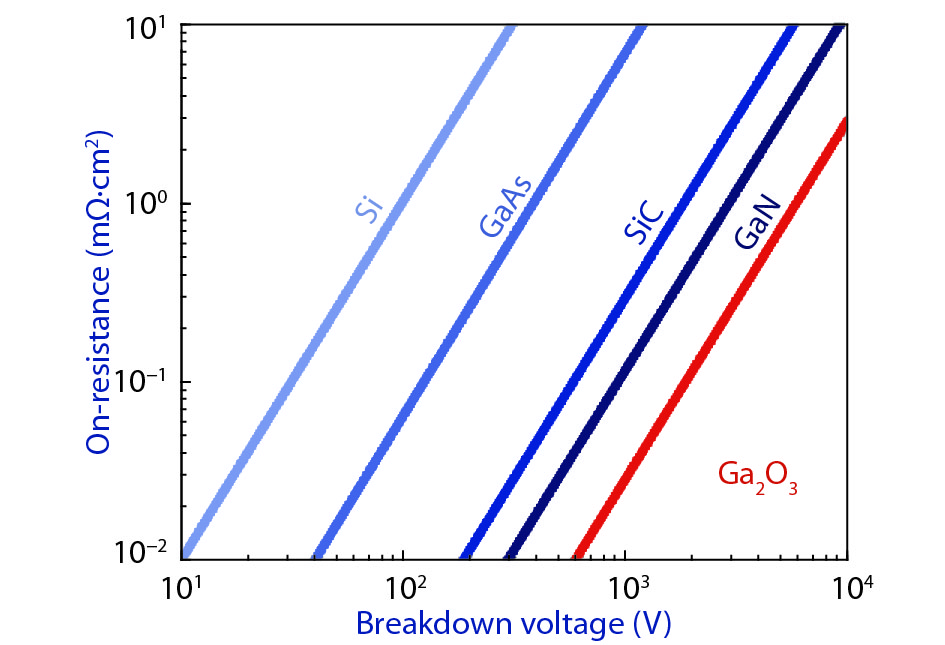
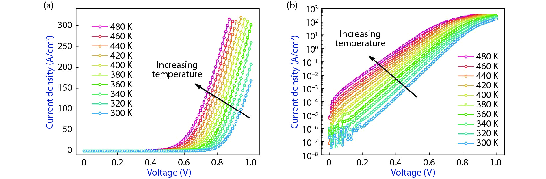
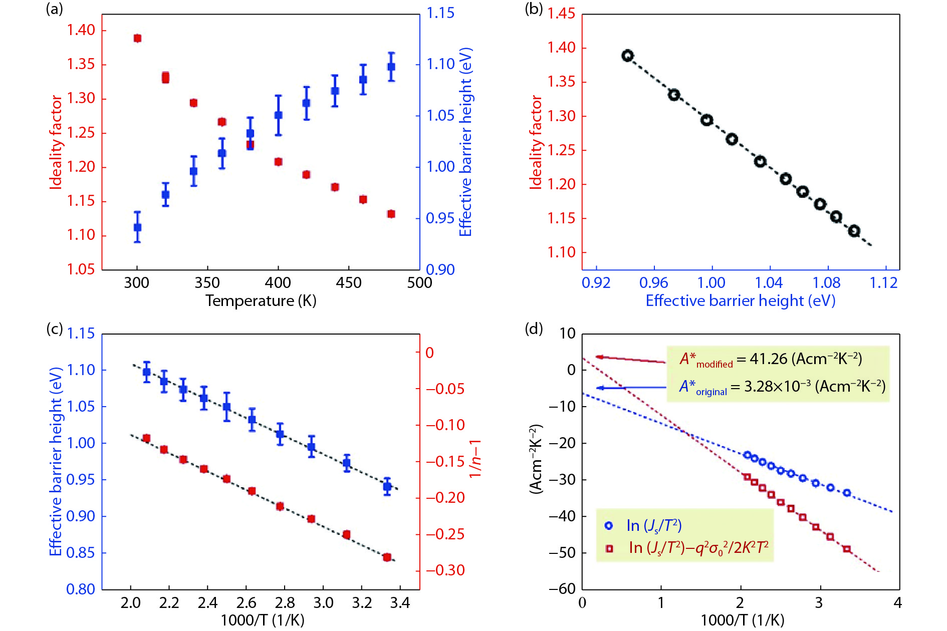
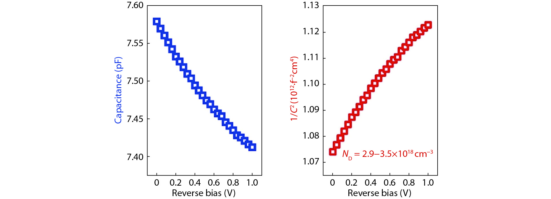
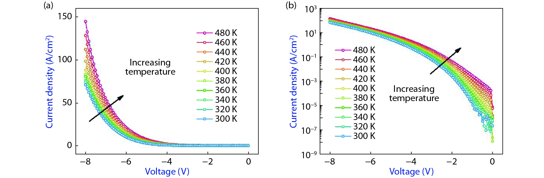
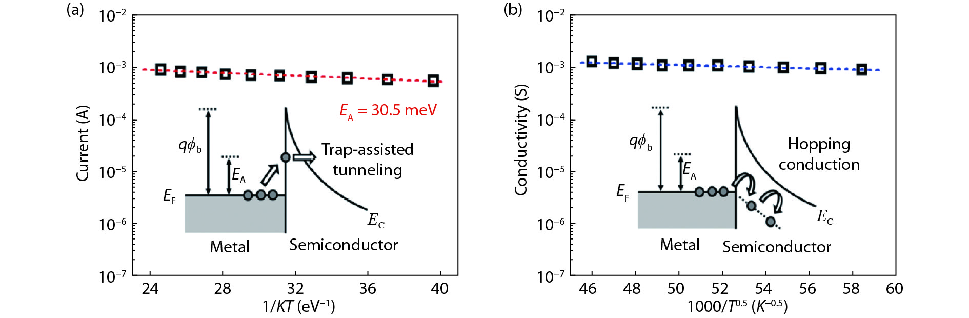
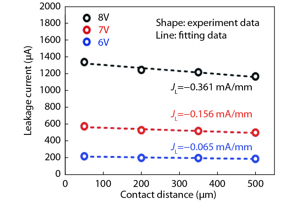
Beta-phase gallium oxide (β-Ga2O3) Schottky barrier diodes were fabricated on highly doped single-crystal substrates, where their temperature-dependent electrical properties were comprehensively investigated by forward and reverse current density – voltage and capacitance – voltage characterization. Both the Schottky barrier height and the ideality factor showed a temperature-dependence behavior, revealing the inhomogeneous nature of the Schottky barrier interface caused by the interfacial defects. With a voltage-dependent Schottky barrier incorporated into thermionic emission theory, the inhomogeneous barrier model can be further examined. Furthermore, the reverse leakage current was found to be dominated by the bulk leakage currents due to the good material and surface quality. Leakage current per distance was also obtained. These results can serve as important references for designing efficient β-Ga2O3 electronic and optoelectronic devices on highly doped substrates or epitaxial layers.

Key words: gallium oxideSchottky barrier diodepower electronicswide bandgap material


[1]
H Sun, K H Li, C G T Castanedo, et al. HCl flow-induced phase change of α-, β-, and ε- Ga2O3 films grown by MOCVD. Cryst Growth Design, 2018, 18: 2370 doi: 10.1021/acs.cgd.7b01791
[2]
H Sun, C G T Castanedo, K Liu, et al. Valence and conduction band offsets of β-Ga2O3/AlN heterojunction. Appl Phys Lett, 2017, 111: 162105, doi: 10.1063/1.5003930
[3]
Z Zhang, E Farzana, A Arehart, et al. Deep level defects throughout the bandgap of (010) β- Ga2O3 detected by optically and thermally stimulated defect spectroscopy. Appl Phys Lett, 2016, 108: 052105, doi: 10.1063/1.4941429
[4]
Q He, W Mu, H Dong, et al. Schottky barrier diode based on β-Ga2O3 (100) single crystal substrate and its temperature-dependent electrical characteristics. Appl Phys Lett, 2017, 110: 093503, doi: 10.1063/1.4977766
[5]
H Tippins. Optical absorption and photoconductivity in the band edge of β-Ga2O3. Phys Rev, 1965, 140: A316, doi: 10.1103/PhysRev.140.A316
[6]
M Higashiwaki, K Sasaki, A Kuramata, et al. Gallium oxide (Ga2O3) metal-semiconductor field-effect transistors on single-crystal β-Ga2O3 (010) substrates. Appl Phys Lett, 2012, 100: 013504, doi: 10.1063/1.3674287
[7]
M Higashiwaki, K Sasaki, T Kamimura, et al. Depletion-mode Ga2O3 metal–oxide–semiconductor field-effect transistors on β-Ga2O3 (010) substrates and temperature dependence of their device characteristics. Appl Phys Lett, 2013, 103: 123511, doi: 10.1063/1.4821858
[8]
T Oishi, Y Koga, K Harada, et al. High-mobility β-Ga2O3 ( ˉ2 01) single crystals grown by edge-defined film-fed growth method and their Schottky barrier diodes with Ni contact. Appl Phys Express, 2015, 8: 031101, doi: 10.7567/APEX.8.031101
[9]
A Kuramata, K Koshi, S Watanabe, et al. High-quality β-Ga2O3 single crystals grown by edge-defined film-fed growth. Jpn J Appl Phys, 2016, 55: 1202A2,
[10]
T Oishi, K Harada, Y Koga, et al. Conduction mechanism in highly doped β-Ga2O3 single crystals grown by edge-defined film-fed growth method and their Schottky barrier diodes. Jpn J Appl Phys, 2016, 55: 030305, doi: 10.7567/JJAP.55.030305
[11]
M Higashiwaki, K Konishi, K Sasaki, et al. Temperature-dependent capacitance–voltage and current–voltage characteristics of Pt/Ga2O3 (001) Schottky barrier diodes fabricated on n-Ga2O3 drift layers grown by halide vapor phase epitaxy. Appl Phys Lett, 2016, 108: 133503, doi: 10.1063/1.4945267
[12]
S Oh, M A Mastro, M J Tadjer, et al. Solar-blind metal-semiconductor-metal photodetectors based on an exfoliated β-Ga2O3 micro-flake. ECS J Solid State Sci Technol, 2017, 6: Q79 doi: 10.1149/2.0231708jss
[13]
M Higashiwaki, K Sasaki, A Kuramata, et al. Development of gallium oxide power devices. Phys Status Solidi A, 2014, 211: 21 doi: 10.1002/pssa.201330197
[14]
K Sasaki, A. Kuramata, T Masui, et al. Device-quality β-Ga2O3 epitaxial films fabricated by ozone moleular beam epitaxy. Appl Phys Express, 2012, 5: 035502, doi: 10.1143/APEX.5.035502
[15]
S Ahn, F Ren, L Yuan, et al. Temperature-dependent characteristics of Ni/Au and Pt/Au Schottky diodes on β-Ga2O3. ECS J Solid State Sci Technol, 2017, 6: P68 doi: 10.1149/2.0291701jss
[16]
K Sasaki, D Wakimoto, Q T Thieu, et al. First demonstration of Ga2O3 trench MOS-type Schottky barrier diodes. IEEE Electron Device Lett, 2017, 38: 783 doi: 10.1109/LED.2017.2696986
[17]
J Yang, S Ahn, F Ren, et al. High reverse breakdown voltage Schottky rectifiers without edge termination on Ga2O3. Appl Phys Lett, 2017, 110: 192101, doi: 10.1063/1.4983203
[18]
K Sasaki, M Higashiwaki, A Kuramata, et al. Ga2O3 Schottky barrier diodes fabricated by using single-crystal β-Ga2O3 (010) substrates. IEEE Electron Device Lett, 2013, 34: 493 doi: 10.1109/LED.2013.2244057
[19]
J Yang, S Ahn, F Ren, et al. High breakdown voltage (−201) β-Ga2O3 Schottky rectifiers. IEEE Electron Device Lett, 2017, 38: 906, doi: 10.1109/LED.2017.2703609
[20]
B Song, A K Verma, K Nomoto, et al. Vertical Ga2O3 Schottky barrier diodes on single-crystal β-Ga2O3 (−201) substrates. Device Research Conference (DRC), 2016, 2016: 1
[21]
H Fu, X Huang, H Chen, et al. Ultra-low turn-on voltage and on-resistance vertical GaN-on-GaN Schottky power diodes with high mobility double drift layers. Appl Phys Lett, 2017, 111: 152102, doi: 10.1063/1.4993201
[22]
F Iucolano, F. Roccaforte, F Giannazzo, et al. Barrier inhomogeneity and electrical properties of Pt/Ga N Shottky contacts. J Appl Phys, 2007, 102: 113701, doi: 10.1063/1.2817647
[23]
Y Son, R L Peterson. The effects of localized tail states on charge transport mechanisms in amorphous zinc tin oxide Schottky diodes. Semicond Sci Technol, 2017, 32: 12LT02,
[24]
D H Lee, K Nomura, T Kamiya, et al. Diffusion-limited a-IGZO/Pt Schottky junction fabricated at 200 °C on a flexible substrate. IEEE Electron Device Lett, 2011, 32: 1695 doi: 10.1109/LED.2011.2167123
[25]
J H Werner, H H Güttler. Barrier inhomogeneities at Schottky contacts. J Appl Phys, 1991, 69: 1522, doi: 10.1063/1.347243
[26]
H von Wenckstern, G Biehne, R A Rahman, et al. Mean barrier height of Pd Schottky contacts on ZnO thin films. Appl Phys Lett, 2006, 88: 092102, doi: 10.1063/1.2180445
[27]
H Fu, I Baranowski, X Huang, et al. Demonstration of AlN Schottky barrier diodes with blocking voltage over 1 kV. IEEE Electron Device Lett, 2017, 38: 1286, doi: 10.1109/LED.2017.2723603
[28]
E Miller, E Yu, P Waltereit, et al. Analysis of reverse-bias leakage current mechanisms in GaN grown by molecular-beam epitaxy. Appl Phys Lett, 2004, 84: 535, doi: 10.1063/1.1644029
[29]
F Padovani, R Stratton Field and thermionic-field emission in Schottky barriers. Solid-State Electron, 1966, 9: 695 doi: 10.1016/0038-1101(66)90097-9
[30]
E Miller, X Dang, E Yu Gate leakage current mechanisms in AlGaN/GaN heterostructure field-effect transistors. J Appl Phys, 2000, 88: 5951 doi: 10.1063/1.1319972
[31]
H Iwano, S Zaima, Y Yasuda. Hopping conduction and localized states in p-Si wires formed by focused ion beam implantations. J Vac Sci Technol B, 1998, 16: 2551 doi: 10.1116/1.590208
[32]
W Lu, L Wang, S Gu, et al. Analysis of reverse leakage current and breakdown voltage in GaN and InGaN/GaN Schottky barriers. IEEE Trans Electron Devices, 2011, 58: 1986 doi: 10.1109/TED.2011.2146254
[33]
H Fu, X Huang, H Chen, et al. Fabrication and characterization of ultra-wide bandgap AlN-based Schottky diodes on sapphire by MOCVD. IEEE J Electron Devices Soc, 2017, 5: 518 doi: 10.1109/JEDS.2017.2751554
[34]
T Loh, H Nguyen, R Murthy, et al. Selective epitaxial germanium on silicon-on-insulator high speed photodetectors using low-temperature ultrathin Si0.8Ge0.2 buffer. Appl Phys Lett, 2007, 91: 073503, doi: 10.1063/1.2769750
[35]
D Yu, C Wang, B L Wehrenberg, et al. Variable range hopping conduction in semiconductor nanocrystal solids. Phys Rev Lett, 2004, 92: 216802 doi: 10.1103/PhysRevLett.92.216802
Fig. 1.  (Color online) Theoretical benchmark plot of on-resistance versus breakdown voltage for power devices based on β-Ga2O3 and other major semiconductors.

Fig. 2.  (Color online) (a) The rocking curve of the β-Ga2O3 substrates measured by HRXRD. (b) The 2D and 3D AFM images of the surface morphology of the β-Ga2O3 substrates. (c) Top and cross-section view of the fabricated SBDs.

Fig. 4.  (Color online) (a) Comparision of on-resistance of previously reported β-Ga2O3 SBDs on various crystal orientations. (b) The turn-on voltage was obtained by linear extrapolation of the linear I–V curves.

Fig. 3.  (Color online) Temperature-dependent forward J–V characteristics of β-Ga2O3 SBDs in (a) linear scale and (b) log scale.

Fig. 5.  (Color online) (a) Ideality factor and Schottky barrier height as a function of temperature from 300 to 480 K. (b) Ideality factor versus Schottky barrier height. (c) Plot of effective barrier height and n−1–1 versus 1000/T with error bars. (d) Original and modified Richardson plot for β-Ga2O3 SBDs. The dashed line shows the fitting curve.

Fig. 6.  (Color online) C-V characteristics for β-Ga2O3 SBDs at 1 MHz. The doping concentration of the devices was also extracted.

Fig. 7.  (Color online) Temperature-dependent reverse J–V characteristics of the β-Ga2O3 SBDs in the (a) linear scale and (b) log scale.

Fig. 8.  (Color online) (a) Arrhenius plot of reverse leakage currents of the β-Ga2O3 SBDs with the activation energy extracted. (b) Conductivity as a function of 1/T1/2 for the β-Ga2O3 SBDs. The inset shows the electron transport in the 1D-VRH conduction model.

Fig. 9.  (Color online) Leakage current as a function of contact distance between ohmic and Schottky contacts at different reverse voltages.

[1]
H Sun, K H Li, C G T Castanedo, et al. HCl flow-induced phase change of α-, β-, and ε- Ga2O3 films grown by MOCVD. Cryst Growth Design, 2018, 18: 2370 doi: 10.1021/acs.cgd.7b01791
[2]
H Sun, C G T Castanedo, K Liu, et al. Valence and conduction band offsets of β-Ga2O3/AlN heterojunction. Appl Phys Lett, 2017, 111: 162105, doi: 10.1063/1.5003930
[3]
Z Zhang, E Farzana, A Arehart, et al. Deep level defects throughout the bandgap of (010) β- Ga2O3 detected by optically and thermally stimulated defect spectroscopy. Appl Phys Lett, 2016, 108: 052105, doi: 10.1063/1.4941429
[4]
Q He, W Mu, H Dong, et al. Schottky barrier diode based on β-Ga2O3 (100) single crystal substrate and its temperature-dependent electrical characteristics. Appl Phys Lett, 2017, 110: 093503, doi: 10.1063/1.4977766
[5]
H Tippins. Optical absorption and photoconductivity in the band edge of β-Ga2O3. Phys Rev, 1965, 140: A316, doi: 10.1103/PhysRev.140.A316
[6]
M Higashiwaki, K Sasaki, A Kuramata, et al. Gallium oxide (Ga2O3) metal-semiconductor field-effect transistors on single-crystal β-Ga2O3 (010) substrates. Appl Phys Lett, 2012, 100: 013504, doi: 10.1063/1.3674287
[7]
M Higashiwaki, K Sasaki, T Kamimura, et al. Depletion-mode Ga2O3 metal–oxide–semiconductor field-effect transistors on β-Ga2O3 (010) substrates and temperature dependence of their device characteristics. Appl Phys Lett, 2013, 103: 123511, doi: 10.1063/1.4821858
[8]
T Oishi, Y Koga, K Harada, et al. High-mobility β-Ga2O3 ( ˉ2 01) single crystals grown by edge-defined film-fed growth method and their Schottky barrier diodes with Ni contact. Appl Phys Express, 2015, 8: 031101, doi: 10.7567/APEX.8.031101
[9]
A Kuramata, K Koshi, S Watanabe, et al. High-quality β-Ga2O3 single crystals grown by edge-defined film-fed growth. Jpn J Appl Phys, 2016, 55: 1202A2,
[10]
T Oishi, K Harada, Y Koga, et al. Conduction mechanism in highly doped β-Ga2O3 single crystals grown by edge-defined film-fed growth method and their Schottky barrier diodes. Jpn J Appl Phys, 2016, 55: 030305, doi: 10.7567/JJAP.55.030305
[11]
M Higashiwaki, K Konishi, K Sasaki, et al. Temperature-dependent capacitance–voltage and current–voltage characteristics of Pt/Ga2O3 (001) Schottky barrier diodes fabricated on n-Ga2O3 drift layers grown by halide vapor phase epitaxy. Appl Phys Lett, 2016, 108: 133503, doi: 10.1063/1.4945267
[12]
S Oh, M A Mastro, M J Tadjer, et al. Solar-blind metal-semiconductor-metal photodetectors based on an exfoliated β-Ga2O3 micro-flake. ECS J Solid State Sci Technol, 2017, 6: Q79 doi: 10.1149/2.0231708jss
[13]
M Higashiwaki, K Sasaki, A Kuramata, et al. Development of gallium oxide power devices. Phys Status Solidi A, 2014, 211: 21 doi: 10.1002/pssa.201330197
[14]
K Sasaki, A. Kuramata, T Masui, et al. Device-quality β-Ga2O3 epitaxial films fabricated by ozone moleular beam epitaxy. Appl Phys Express, 2012, 5: 035502, doi: 10.1143/APEX.5.035502
[15]
S Ahn, F Ren, L Yuan, et al. Temperature-dependent characteristics of Ni/Au and Pt/Au Schottky diodes on β-Ga2O3. ECS J Solid State Sci Technol, 2017, 6: P68 doi: 10.1149/2.0291701jss
[16]
K Sasaki, D Wakimoto, Q T Thieu, et al. First demonstration of Ga2O3 trench MOS-type Schottky barrier diodes. IEEE Electron Device Lett, 2017, 38: 783 doi: 10.1109/LED.2017.2696986
[17]
J Yang, S Ahn, F Ren, et al. High reverse breakdown voltage Schottky rectifiers without edge termination on Ga2O3. Appl Phys Lett, 2017, 110: 192101, doi: 10.1063/1.4983203
[18]
K Sasaki, M Higashiwaki, A Kuramata, et al. Ga2O3 Schottky barrier diodes fabricated by using single-crystal β-Ga2O3 (010) substrates. IEEE Electron Device Lett, 2013, 34: 493 doi: 10.1109/LED.2013.2244057
[19]
J Yang, S Ahn, F Ren, et al. High breakdown voltage (−201) β-Ga2O3 Schottky rectifiers. IEEE Electron Device Lett, 2017, 38: 906, doi: 10.1109/LED.2017.2703609
[20]
B Song, A K Verma, K Nomoto, et al. Vertical Ga2O3 Schottky barrier diodes on single-crystal β-Ga2O3 (−201) substrates. Device Research Conference (DRC), 2016, 2016: 1
[21]
H Fu, X Huang, H Chen, et al. Ultra-low turn-on voltage and on-resistance vertical GaN-on-GaN Schottky power diodes with high mobility double drift layers. Appl Phys Lett, 2017, 111: 152102, doi: 10.1063/1.4993201
[22]
F Iucolano, F. Roccaforte, F Giannazzo, et al. Barrier inhomogeneity and electrical properties of Pt/Ga N Shottky contacts. J Appl Phys, 2007, 102: 113701, doi: 10.1063/1.2817647
[23]
Y Son, R L Peterson. The effects of localized tail states on charge transport mechanisms in amorphous zinc tin oxide Schottky diodes. Semicond Sci Technol, 2017, 32: 12LT02,
[24]
D H Lee, K Nomura, T Kamiya, et al. Diffusion-limited a-IGZO/Pt Schottky junction fabricated at 200 °C on a flexible substrate. IEEE Electron Device Lett, 2011, 32: 1695 doi: 10.1109/LED.2011.2167123
[25]
J H Werner, H H Güttler. Barrier inhomogeneities at Schottky contacts. J Appl Phys, 1991, 69: 1522, doi: 10.1063/1.347243
[26]
H von Wenckstern, G Biehne, R A Rahman, et al. Mean barrier height of Pd Schottky contacts on ZnO thin films. Appl Phys Lett, 2006, 88: 092102, doi: 10.1063/1.2180445
[27]
H Fu, I Baranowski, X Huang, et al. Demonstration of AlN Schottky barrier diodes with blocking voltage over 1 kV. IEEE Electron Device Lett, 2017, 38: 1286, doi: 10.1109/LED.2017.2723603
[28]
E Miller, E Yu, P Waltereit, et al. Analysis of reverse-bias leakage current mechanisms in GaN grown by molecular-beam epitaxy. Appl Phys Lett, 2004, 84: 535, doi: 10.1063/1.1644029
[29]
F Padovani, R Stratton Field and thermionic-field emission in Schottky barriers. Solid-State Electron, 1966, 9: 695 doi: 10.1016/0038-1101(66)90097-9
[30]
E Miller, X Dang, E Yu Gate leakage current mechanisms in AlGaN/GaN heterostructure field-effect transistors. J Appl Phys, 2000, 88: 5951 doi: 10.1063/1.1319972
[31]
H Iwano, S Zaima, Y Yasuda. Hopping conduction and localized states in p-Si wires formed by focused ion beam implantations. J Vac Sci Technol B, 1998, 16: 2551 doi: 10.1116/1.590208
[32]
W Lu, L Wang, S Gu, et al. Analysis of reverse leakage current and breakdown voltage in GaN and InGaN/GaN Schottky barriers. IEEE Trans Electron Devices, 2011, 58: 1986 doi: 10.1109/TED.2011.2146254
[33]
H Fu, X Huang, H Chen, et al. Fabrication and characterization of ultra-wide bandgap AlN-based Schottky diodes on sapphire by MOCVD. IEEE J Electron Devices Soc, 2017, 5: 518 doi: 10.1109/JEDS.2017.2751554
[34]
T Loh, H Nguyen, R Murthy, et al. Selective epitaxial germanium on silicon-on-insulator high speed photodetectors using low-temperature ultrathin Si0.8Ge0.2 buffer. Appl Phys Lett, 2007, 91: 073503, doi: 10.1063/1.2769750
[35]
D Yu, C Wang, B L Wehrenberg, et al. Variable range hopping conduction in semiconductor nanocrystal solids. Phys Rev Lett, 2004, 92: 216802 doi: 10.1103/PhysRevLett.92.216802
1

Improvement of Ga2O3 vertical Schottky barrier diode by constructing NiO/Ga2O3 heterojunction

Xueqiang Ji, Jinjin Wang, Song Qi, Yijie Liang, Shengrun Hu, et al.

Journal of Semiconductors, 2024, 45(4): 042503. doi: 10.1088/1674-4926/45/4/042503

2

Anisotropic optical and electric properties of β-gallium oxide

Yonghui Zhang, Fei Xing

Journal of Semiconductors, 2023, 44(7): 071801. doi: 10.1088/1674-4926/44/7/071801

3

Optimization of recess-free AlGaN/GaN Schottky barrier diode by TiN anode and current transport mechanism analysis

Hao Wu, Xuanwu Kang, Yingkui Zheng, Ke Wei, Lin Zhang, et al.

Journal of Semiconductors, 2022, 43(6): 062803. doi: 10.1088/1674-4926/43/6/062803

4

Investigation of lateral spreading current in the 4H-SiC Schottky barrier diode chip

Xi Wang, Yiwen Zhong, Hongbin Pu, Jichao Hu, Xianfeng Feng, et al.

Journal of Semiconductors, 2021, 42(11): 112802. doi: 10.1088/1674-4926/42/11/112802

5

Thermally annealed gamma irradiated Ni/4H-SiC Schottky barrier diode characteristics

P. Vigneshwara Raja, N. V. L. Narasimha Murty

Journal of Semiconductors, 2019, 40(2): 022804. doi: 10.1088/1674-4926/40/2/022804

6

Hot electron effects on the operation of potential well barrier diodes

M. Akura, G. Dunn, M. Missous

Journal of Semiconductors, 2019, 40(12): 122101. doi: 10.1088/1674-4926/40/12/122101

7

A review of the most recent progresses of state-of-art gallium oxide power devices

Hong Zhou, Jincheng Zhang, Chunfu Zhang, Qian Feng, Shenglei Zhao, et al.

Journal of Semiconductors, 2019, 40(1): 011803. doi: 10.1088/1674-4926/40/1/011803

8

Engineering in-plane silicon nanowire springs for highly stretchable electronics

Zhaoguo Xue, Taige Dong, Zhimin Zhu, Yaolong Zhao, Ying Sun, et al.

Journal of Semiconductors, 2018, 39(1): 011001. doi: 10.1088/1674-4926/39/1/011001

9

Lateral polarity control of III-nitride thin film and application in GaN Schottky barrier diode

Junmei Li, Wei Guo, Moheb Sheikhi, Hongwei Li, Baoxue Bo, et al.

Journal of Semiconductors, 2018, 39(5): 053003. doi: 10.1088/1674-4926/39/5/053003

10

Hybrid functional microfibers for textile electronics and biosensors

Bichitra Nanda Sahoo, Byungwoo Choi, Jungmok Seo, Taeyoon Lee

Journal of Semiconductors, 2018, 39(1): 011009. doi: 10.1088/1674-4926/39/1/011009

11

Materials and applications of bioresorbable electronics

Xian Huang

Journal of Semiconductors, 2018, 39(1): 011003. doi: 10.1088/1674-4926/39/1/011003

12

Schottky barrier parameters and structural properties of rapidly annealed Zr Schottky electrode on p-type GaN

V. Rajagopal Reddy, B. Asha, Chel-Jong Choi

Journal of Semiconductors, 2017, 38(6): 064001. doi: 10.1088/1674-4926/38/6/064001

13

Influences of ICP etching damages on the electronic properties of metal field plate 4H-SiC Schottky diodes

Hui Wang, Yingxi Niu, Fei Yang, Yong Cai, Zehong Zhang, et al.

Journal of Semiconductors, 2015, 36(10): 104006. doi: 10.1088/1674-4926/36/10/104006

14

Inhomogeneous barrier height effect on the current-voltage characteristics of an Au/n-InP Schottky diode

Kamal Zeghdar, Lakhdar Dehimi, Achour Saadoune, Nouredine Sengouga

Journal of Semiconductors, 2015, 36(12): 124002. doi: 10.1088/1674-4926/36/12/124002

15

Comment on Chen et al. "Fabrication and photovoltaic conversion enhancement of graphene/n-Si Schottky barrier solar cells by electrophoretic deposition", Electrochimica Acta, 2014

Lara Valentic, Nima E. Gorji

Journal of Semiconductors, 2015, 36(9): 094012. doi: 10.1088/1674-4926/36/9/094012

16

In situ TEM/SEM electronic/mechanical characterization of nano material with MEMS chip

Yuelin Wang, Tie Li, Xiao Zhang, Hongjiang Zeng, Qinhua Jin, et al.

Journal of Semiconductors, 2014, 35(8): 081001. doi: 10.1088/1674-4926/35/8/081001

17

Fabrication and characteristics of a 4H-SiC junction barrier Schottky diode

Chen Fengping, Zhang Yuming, Lü Hongliang, Zhang Yimen, Guo Hui, et al.

Journal of Semiconductors, 2011, 32(6): 064003. doi: 10.1088/1674-4926/32/6/064003

18

Barrier height and ideality factor dependency on identically produced small Au/p-Si Schottky barrier diodes

M. A. Yeganeh, S. H. Rahmatollahpur

Journal of Semiconductors, 2010, 31(7): 074001. doi: 10.1088/1674-4926/31/7/074001

19

(NH4)2S treatment of the Si (100) surface and its effects on Al/Si Schottky barrier heights

Hu Aibin, Wang Wenwu, Xu Qiuxia

Journal of Semiconductors, 2009, 30(8): 084001. doi: 10.1088/1674-4926/30/8/084001

20

Optimized design of 4H-SiC floating junction power Schottky barrier diodes

Pu Hongbin, Cao Lin, Chen Zhiming, Ren Jie

Journal of Semiconductors, 2009, 30(4): 044001. doi: 10.1088/1674-4926/30/4/044001

1. Kumari, M., Roul, B., Krupanidhi, S.B. et al. Heterostructuring approach to enhance figures-of-merit of Ga2O3 for deep UV photodetection. Physica B: Condensed Matter, 2025. doi:10.1016/j.physb.2025.417267
2. Ravendra, P., Raman, A., Ranjan, R. et al. Design, Simulation, and Comparison of p-GaN-based β-Ga2O3 FET on Wide Bandgap Substrates. Semiconductors, 2025, 59(4): 328-336. doi:10.1134/S1063782624602152
3. Hein, P., Romstadt, T., Draber, F. et al. Variable-Range Hopping Conduction in Amorphous, Non-Stoichiometric Gallium Oxide. Advanced Electronic Materials, 2025, 11(4): 2400407. doi:10.1002/aelm.202400407
4. Li, J., Zhang, G., Wu, Y. Transparent rare earth-doped gallium oxide ceramics with oriented microstructure. Journal of the American Ceramic Society, 2025, 108(1): e20121. doi:10.1111/jace.20121
5. Ganguly, S., Nama Manjunatha, K., Paul, S. Advances in Gallium Oxide: Properties, Applications, and Future Prospects. Advanced Electronic Materials, 2025. doi:10.1002/aelm.202400690
6. Li, M., He, M., Wang, X. et al. High-performance β-Ga2O3 Schottky barrier diodes with Mg current blocking layer using spin-on-glass technique. Applied Physics Letters, 2024, 125(13): 132101. doi:10.1063/5.0230034
7. Labed, M., Meftah, A., Sengouga, N. et al. Modeling temperature dependent Ni/β-Ga2O3 Schottky barrier diode interface properties. Materials Science and Engineering: B, 2024. doi:10.1016/j.mseb.2024.117485
8. Wang, Z.P., Sun, N., Yu, X.X. et al. Performance limiting inhomogeneities of defect states in ampere-class Ga2O3 power diodes. Applied Physics Reviews, 2024, 11(2) doi:10.1063/5.0191343
9. Spencer, J.A., Jacobs, A.G., Hobart, K.D. et al. PtOx Schottky Contacts on Degenerately Doped 2¯01β-Ga2O3 Substrates. Journal of Electronic Materials, 2024, 53(6): 2798-2805. doi:10.1007/s11664-024-10966-5
10. He, Y., Zhao, F., Huang, B. et al. A Review of β-Ga2O3 Power Diodes. Materials, 2024, 17(8): 1870. doi:10.3390/ma17081870
11. Islam, M.E., Shimamoto, K., Yoshimura, T. et al. Dielectric properties of low-temperature-grown homoepitaxial (−201) β-Ga2O3 thin film by atmospheric pressure plasma-assisted CVD. AIP Advances, 2024, 14(4): 045003. doi:10.1063/5.0189793
12. Xu, W., Shen, Z., Qu, Z. et al. Current transport mechanism of lateral Schottky barrier diodes on β-Ga2O3/SiC structure with atomic level interface. Applied Physics Letters, 2024, 124(11): 112102. doi:10.1063/5.0196517
13. Paul, S., Lopez, R., Neal, A.T. et al. Low-temperature electrical properties and barrier inhomogeneities in ITO/β-Ga2O3 Schottky diode. Journal of Vacuum Science and Technology B, 2024, 42(2): 024004. doi:10.1116/6.0003401
14. Fardi, H.. Modeling interface charges in Al2O3/Ga2O3 normallyon n-channel field effect transistors. 2024. doi:10.1109/INTCEC61833.2024.10603144
15. Labed, M., Min, J.Y., Slim, A.B. et al. Tunneling via surface dislocation in W/β-Ga2O3 Schottky barrier diodes. Journal of Semiconductors, 2023, 44(7): 072801. doi:10.1088/1674-4926/44/7/072801
16. P. Sundaram, P., Liu, F., Alema, F. et al. Characterization of (001) β-Ga2O3 Schottky diodes with drift layer grown by MOCVD. Applied Physics Letters, 2023, 122(23): 232105. doi:10.1063/5.0155622
17. Gao, S., Yang, X., Cheng, J. et al. Deformation and fracture behaviors of monocrystalline β-Ga2O3 characterized using indentation method and first-principles calculations. Materials Characterization, 2023. doi:10.1016/j.matchar.2023.112920
18. Mudiyanselage, D.H., Wang, D., Fu, H. Ultrawide bandgap vertical β-(Al xGa1 -x )2O3Schottky barrier diodes on free-standing β-Ga2O3substrates. Journal of Vacuum Science and Technology A: Vacuum, Surfaces and Films, 2023, 41(2): 023201. doi:10.1116/6.0002265
19. Sood, A., Wuu, D.-S., Tarntair, F.-G. et al. Electrical performance study of Schottky barrier diodes using ion implanted β-Ga2O3 epilayers grown on sapphire substrates. Materials Today Advances, 2023. doi:10.1016/j.mtadv.2023.100346
20. Patnaik, A., Gupta, M., Sharma, P. Forward Bias Gate Leakage Mechanism in δ-doped β-(AlxGa1-x)2O3/Ga2O3HFET. 2023. doi:10.1109/MIEL58498.2023.10315896
21. Lyle, L.A.M.. Critical review of Ohmic and Schottky contacts to β-Ga2O3. Journal of Vacuum Science and Technology A: Vacuum, Surfaces and Films, 2022, 40(6): 060802. doi:10.1116/6.0002144
22. Shivani, Kaur, D., Ghosh, A., Kumar, M. A strategic review on gallium oxide based power electronics: Recent progress and future prospects. Materials Today Communications, 2022. doi:10.1016/j.mtcomm.2022.104244
23. P. Sundaram, P., Alema, F., Osinsky, A. et al. β-(Al xGa1- x )2O3/Ga2O3heterostructure Schottky diodes for improved v BR2/ R ON. Journal of Vacuum Science and Technology A: Vacuum, Surfaces and Films, 2022, 40(4): 043211. doi:10.1116/6.0001907
24. Sheoran, H., Kumar, V., Singh, R. A Comprehensive Review on Recent Developments in Ohmic and Schottky Contacts on Ga2O3for Device Applications. ACS Applied Electronic Materials, 2022, 4(6): 2589-2628. doi:10.1021/acsaelm.2c00101
25. Kim, H.. Control and understanding of metal contacts to β-Ga2O3 single crystals: a review. SN Applied Sciences, 2022, 4(1): 27. doi:10.1007/s42452-021-04895-9
26. Wang, X., Zhang, S., Huo, X. et al. Research Progress of Ultra-Wide Bandgap Semiconductor β-Ga2O3 | [超宽禁带半导体β-Ga2O3相关研究进展]. Rengong Jingti Xuebao/Journal of Synthetic Crystals, 2021, 50(11): 1995-2012.
27. Xia, X., Xian, M., Fares, C. et al. Temperature dependent performance of ITO Schottky contacts on β-Ga2O3. Journal of Vacuum Science and Technology A: Vacuum, Surfaces and Films, 2021, 39(5): 053405. doi:10.1116/6.0001211
28. Heinselman, K., Walker, P., Norman, A. et al. Performance and reliability of β-Ga2O3Schottky barrier diodes at high temperature. Journal of Vacuum Science and Technology A: Vacuum, Surfaces and Films, 2021, 39(4): 040402. doi:10.1116/6.0001003
29. He, M., Cheng, W.-C., Zeng, F. et al. Improvement of β-GaO3 MIS-SBD Interface Using Al-Reacted Interfacial Layer. IEEE Transactions on Electron Devices, 2021, 68(7): 3314-3319. doi:10.1109/TED.2021.3081075
30. Xia, X., Xian, M., Carey, P. et al. Vertical β-Ga2O3Schottky rectifiers with 750 v reverse breakdown voltage at 600 K. Journal of Physics D: Applied Physics, 2021, 54(30): 305103. doi:10.1088/1361-6463/abfe37
31. Kaur, D., Kumar, M. A Strategic Review on Gallium Oxide Based Deep-Ultraviolet Photodetectors: Recent Progress and Future Prospects. Advanced Optical Materials, 2021, 9(9): 2002160. doi:10.1002/adom.202002160
32. Labed, M., Sengouga, N., Labed, M. et al. Modeling and analyzing temperature-dependent parameters of Ni/β-Ga2O3Schottky barrier diode deposited by confined magnetic field-based sputtering. Semiconductor Science and Technology, 2021, 36(3): 035020. doi:10.1088/1361-6641/abe059
33. Li, W., Jena, D., Xing, H.G. Advanced concepts in Ga2O3 power and RF devices. Semiconductors and Semimetals, 2021. doi:10.1016/bs.semsem.2021.04.002
34. Cimilli Çatir, F.E.. Properties of a facile growth of spray pyrolysis-based rGO films and device performance for Au/rGO/n-InP Schottky diodes. Journal of Materials Science: Materials in Electronics, 2021, 32(1): 611-622. doi:10.1007/s10854-020-04843-0
35. Shi, F., Qiao, H. Photoluminescence property of Cr-doped β-Ga2O3nanorods synthesized by a hydrothermal method. CrystEngComm, 2020, 22(45): 7794-7799. doi:10.1039/d0ce01416h
36. Buttay, C., Wong, H.-Y., Wang, B. et al. Surge current capability of ultra-wide-bandgap Ga2O3 Schottky diodes. Microelectronics Reliability, 2020. doi:10.1016/j.microrel.2020.113743
37. Islam, Z., Xian, M., Haque, A. et al. In Situ Observation of β-Ga 2 O 3 Schottky Diode Failure under Forward Biasing Condition. IEEE Transactions on Electron Devices, 2020, 67(8): 3056-3061. doi:10.1109/TED.2020.3000441
38. Li, W., Saraswat, D., Long, Y. et al. Near-ideal reverse leakage current and practical maximum electric field in β-Ga2O3Schottky barrier diodes. Applied Physics Letters, 2020, 116(19): 192101. doi:10.1063/5.0007715
39. Sheoran, H., Tak, B.R., Manikanthababu, N. et al. Temperature-Dependent Electrical Characteristics of Ni/Au Vertical Schottky Barrier Diodes on β-Ga2O3 Epilayers. ECS Journal of Solid State Science and Technology, 2020, 9(5): 055004. doi:10.1149/2162-8777/ab96ad
40. Yang, T.-H., Fu, H., Fu, K. et al. Vertical GaN-on-GaN Schottky Barrier Diodes with Multi-Floating Metal Rings. IEEE Journal of the Electron Devices Society, 2020. doi:10.1109/JEDS.2020.3014133
41. Alfaraj, N., Min, J.-W., Kang, C.H. et al. Deep-ultraviolet integrated photonic and optoelectronic devices: A prospect of the hybridization of group III-nitrides, III-oxides, and two-dimensional materials. Journal of Semiconductors, 2019, 40(12): 121801. doi:10.1088/1674-4926/40/12/121801
42. Kim, H., Kyoung, S., Kang, T. et al. Effective surface diffusion of nickel on single crystal β-Ga2O3 for Schottky barrier modulation and high thermal stability. Journal of Materials Chemistry C, 2019, 7(35): 10953-10960. doi:10.1039/c9tc02922b
  • Search

    Advanced Search >>

    GET CITATION

    Tsung-Han Yang, Houqiang Fu, Hong Chen, Xuanqi Huang, Jossue Montes, Izak Baranowski, Kai Fu, Yuji Zhao. Temperature-dependent electrical properties of β-Ga2O3 Schottky barrier diodes on highly doped single-crystal substrates[J]. Journal of Semiconductors, 2019, 40(1): 012801. doi: 10.1088/1674-4926/40/1/012801
    T Yang, H Q Fu, H Chen, X Q Huang, J Montes, I Baranowski, K Fu, Y J Zhao, Temperature-dependent electrical properties of β-Ga2O3 Schottky barrier diodes on highly doped single-crystal substrates[J]. J. Semicond., 2019, 40(1): 012801. doi: 10.1088/1674-4926/40/1/012801.
    shu

    Export: BibTex EndNote

    Article Metrics

    Article views: 5721 Times PDF downloads: 355 Times Cited by: 42 Times

    History

    Received: 05 September 2018 Revised: 04 October 2018 Online: Accepted Manuscript: 10 December 2018Uncorrected proof: 13 December 2018Published: 07 January 2019

    Catalog

      Email This Article

      User name:
      Email:*请输入正确邮箱
      Code:*验证码错误
      Tsung-Han Yang, Houqiang Fu, Hong Chen, Xuanqi Huang, Jossue Montes, Izak Baranowski, Kai Fu, Yuji Zhao. Temperature-dependent electrical properties of β-Ga2O3 Schottky barrier diodes on highly doped single-crystal substrates[J]. Journal of Semiconductors, 2019, 40(1): 012801. doi: 10.1088/1674-4926/40/1/012801 ****T Yang, H Q Fu, H Chen, X Q Huang, J Montes, I Baranowski, K Fu, Y J Zhao, Temperature-dependent electrical properties of β-Ga2O3 Schottky barrier diodes on highly doped single-crystal substrates[J]. J. Semicond., 2019, 40(1): 012801. doi: 10.1088/1674-4926/40/1/012801.
      Citation:
      Tsung-Han Yang, Houqiang Fu, Hong Chen, Xuanqi Huang, Jossue Montes, Izak Baranowski, Kai Fu, Yuji Zhao. Temperature-dependent electrical properties of β-Ga2O3 Schottky barrier diodes on highly doped single-crystal substrates[J]. Journal of Semiconductors, 2019, 40(1): 012801. doi: 10.1088/1674-4926/40/1/012801 ****
      T Yang, H Q Fu, H Chen, X Q Huang, J Montes, I Baranowski, K Fu, Y J Zhao, Temperature-dependent electrical properties of β-Ga2O3 Schottky barrier diodes on highly doped single-crystal substrates[J]. J. Semicond., 2019, 40(1): 012801. doi: 10.1088/1674-4926/40/1/012801.

      Temperature-dependent electrical properties of β-Ga2O3 Schottky barrier diodes on highly doped single-crystal substrates

      DOI: 10.1088/1674-4926/40/1/012801
      More Information
      • Corresponding author: Email: yuji.zhao@asu.edu
      • Received Date: 2018-09-05
      • Revised Date: 2018-10-04
      • Published Date: 2019-01-01

      Catalog

        /

        DownLoad:  Full-Size Img  PowerPoint
        Return
        Return