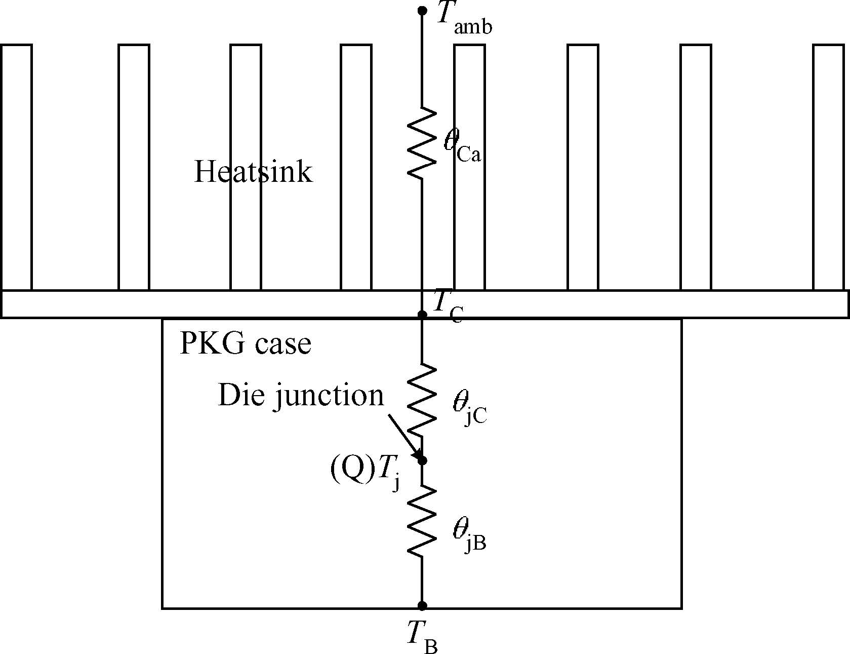
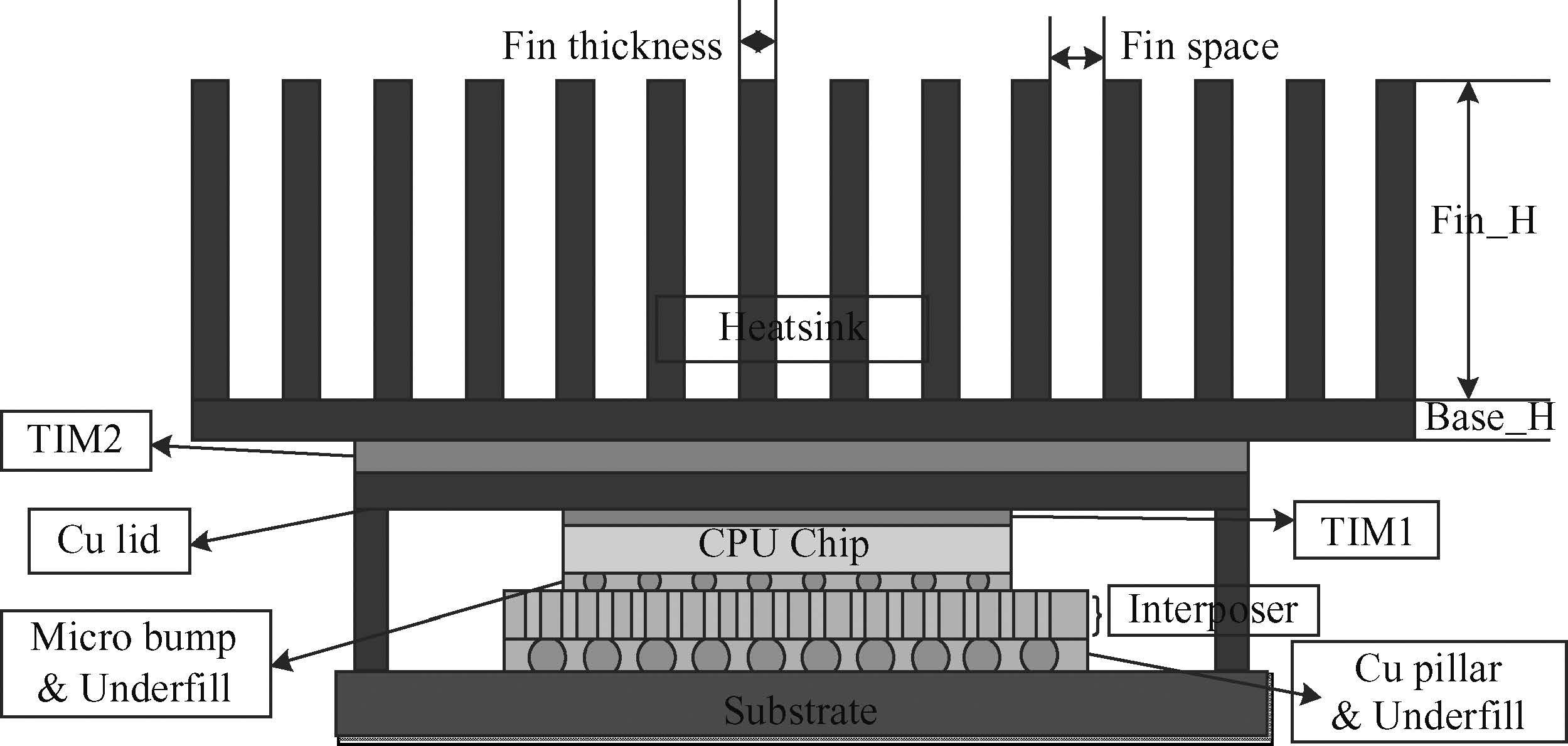
1. Introduction
Flip chip packaging with the conventional organic buildup substrate is facing a bottleneck in fine pitch wiring as the interconnect density is continuing to shrink,and the cost of fabricating finer pitch organic substrate is increasing significantly. To address these demands,the 2.5D package with through silicon via (TSV) interposer has emerged as a good solution to obtain higher package density[1, 2]. The 2.5D integration technology uses emerging shorter interconnection of TSV,finer pitch silicon-silicon interconnections and thinner silicon for die/interposer. This makes the technology widely applicable from simple to very complex applications,with higher density,multi-function and better performance[3].
However,with multi-dies stacked in one package,the thermal management becomes more critical,because of: (1) the extremely high heat flux generated by multifunctional chips in miniature packages; (2) the lack of space between dies for cooling channels; and (3) the unpredictable hot-spots created by TSV and thin chips[4]. All these heat-related issues may lead to device failure in the electronic systems. Hence,to ensure the survival of the overall system,the thermal analysis and optimal design for the 2.5D package is necessary and important.
In this context,numerical simulations,based on ANSYS software,were utilized extensively for thermal performance prediction. The focused 2.5D package contains a functional large CPU chip with more than 9000 bumps and an integrated TSV interposer. The designed CPU chip power would reach as high as 120 W. So the thermal solution for this 2.5D package needs to be analyzed. In the following,parametric studies are conducted to identify the crucial factors for the thermal performance. Finally,an optimization design case for heat dissipation is demonstrated.
2. Finite element modeling (FEM)
The computational model was buildup in ANSYS software. The structure of the packaging is shown in Figure 1,in which the high power chip is connected to the BT substrate through a TSV interposer. The micro bumps under the chip and copper pillars under the interposer connect the chip,interposer and substrate into a whole system,and all these parts are packed in a Cu lid. Meanwhile,a heatsink is added on the package to enhance the heat dissipation ability. The details of the structure size are illustrated in Table 1.
Note: In the table,D,H and P represent diameter,height and pitch,respectively.
To simplify the computation,here we made some assumptions for the FEM model:
(1) Perfect adhesion for all materials interfaces.
(2) Isotropic properties for all materials.
(3) Only 1/4 model was used in the simulation,due to being symmetric.
(4) Effective thermal conduction model[5] was applied to the complex structures,such as silicon interposer + TSVs,Underfill + Bumps and Underfill + Solders. The equivalent thermal conductivities were calculated through the following equations[5]:
Keq,z=βKCu+KSi1+β,β=VCu/VSi, |
(1) |
Keq,x−y=π(1+β)K2Si+KSi(KCu−KSi)√4πβ(1+β)π(1+β)KSi+(KCu−KSi)(√4πβ(1+β)−4β). |
(2) |
Here,K is the thermal conductivity,and V is the total volume for each material.
The thermal properties for all materials,including the effective thermal conductivities,are listed in Table 2.
3. Parametric studies
In this section,series simulations will be done to analyze the effect of some package parameters on the thermal performance of the 2.5D PKG. Here,a compact thermal resistance model,shown in Figure 2,was built to evaluate the thermal simulation results,as thermal resistance is one of the most important and the most common assessment references for thermal management[6, 7].
According to the JEDEC test standards JEDEC51-8,SEMI G30-88,SEMI G38-0996 and SEMI G42-0996,θjB,θjC and θCa are simulated with different thermal boundaries,and a variable Γ was defined to calculate the relative changes of the thermal resistance.
Γ=θ′−θInitθInit×100%. |
The analysis results for θjB,θjC and θCa are marked as ΓjB,ΓjC and ΓCa,respectively.
3.1 Effect of TSV interposer
A TSV interposer is the core structure of the 2.5D package,and also an important part for thermal management. For thermal effects analysis of the interposer,the main focus was concentrated on the TSV diameter and interposer thickness. As the interposer is primarily associated with the thermal resistance θjB,the relationship between interposer parameters and variable ΓjB are plotted,as shown in Figure 3.
Only considering the TSV diameter,an obviously downward trend of ΓjB will occur while the TSV diameter increases,which means a lower resistance of θjB. Moreover,the thinner the TSV interposer is,the greater the effect the TSV diameter would generate. For example,the fluctuation of ΓjB is about 6% when the interposer thickness is 0.5 mm,while this fluctuation will reduce to about 2% with a thickness of 0.3 mm. In general,a thicker interposer and bigger TSV is more favorable for the heat dissipation.
3.2 Effect of substrate
In the assumptions made above,the substrate is treated as an isotropic material,but due to the copper trace layers,the actual thermal conductivity of the substrate is different for in-plane direction Kp and out-of-plane direction Kn. The copper coverage and trace layer thickness have a tiny effect on Kn,[8],so only the effect of Kp was analyzed in the following simulations. Figure 4 displays several curves of ΓjB versus substrate thickness under varying in-plane conductivity of substrate,Kp.
The results show a linear relationship between substrate thickness and ΓjB when the substrate Kp is fixed. Through curve fitting calculations,the scope of these lines changes from 66.15 to 28.00 while the Sub_Kp increases from a minimum value of 0.51 W/(m⋅K) to a maximum value of 390 W/(m⋅K). This indicates that with a lower conductivity,the substrate thickness will have a more significant effect on the thermal resistance of the package.
Noting that,in our analysis,the maximum change value of ΓjB for different interposer parameters is less than ±5%,while this value for the substrate case would reach -75% to 45%. So,the improvement of the substrate will be more helpful for the optimal design of resistance θjB.
3.3 Effect of TIM1
In the package,TIM1 is used to fill the micro spaces between the die and the cu lid,and is the first link of the heat dissipation path. Thermal interface materials could be conductive adhesive,gels,phase change materials,thermal grease,solder or even graphite materials,which have a thermal conductivity range from 0.1 to over 300 W/(m⋅K)[9]. In this section,the curves between ΓjC and TIM1 parameters are plotted,as shown in Figure 5.
These curves are similar to those in Figure 4. Under a certain thermal conductivity,a thinner TIM1 layer is more conducive for heat spread. Meanwhile,the ΓjC is linearly related with the thickness,and the line scope is inversely proportional to the conductivity. The maximum and minimum scopes of the curves are 11174.7 and 116.5,showing that the effect of thickness will be eroded about 100 times when the thermal conductivity of TIM1 increases from 1 to 100 W/(m⋅K).
3.4 Effect of Cu lid
For the analyzed 2.5D high power package,the die is covered by a copper lid,which can provide electromagnetic shielding and physical tightness for the internal devices[10].
The Cu lid structure has an obvious impact on the thermal resistance θjC because of the direct heat exchange with the external environment. In this part,thermal simulations were conducted with different lid sizes and lid thicknesses,and the results are displayed in Figure 6.
In Figure 6,it can be seen that lid size nearly has no effect on the package thermal performance as all the curves almost completely overlap. ΓjC and lid thickness show a certain linear relationship,and can be expressed as:
ΓjC=(29.64×Lid_T−32.62)×100%. |
Here,Lid_T is the lid thickness. The maximum fluctuation of ΓjC observed in Figure 6 is about ±12%,this is relatively small when compared with the result obtained in section C,so it can be concluded that TIM1 is a more significant factor for the package thermal performance.
3.5 Effect of heatsink
For the high power 2.5D package,the heatsink is one of the key parts for heat spreading out and now is widely used in electronic products. The cooling capacity of a heatsink can be reflected by the definition of θCa,which is related to the geometrical characteristics of the heatsink,such as base height (Base_H) and fin height (Fin_H). Figure 7 presents the analysis results of ΓCa with different heatsink heights.
In general,all the curves in Figure 7 show the same tendency: ΓCa benefits from a higher heatsink base and a higher fin. For a fixed fin height,the average decline of ΓCa caused by the base height is only about 20%. Under the same consideration for the fin height,even the minimum decline of ΓCa would reach over 50%,implying a greater effect than base height.
4. Optimal design
Hereinbefore,the influential Factors for θjB,θjC and θCa have been studied respectively. In this section,an orthogonal test method will be used to evaluate these factors and to design the optimal solution[11, 12]. According to the analysis above,three factors are picked up for the orthogonal test: the in-plane conductivity of the substrate (Sub_Kp),thermal conductivity of TIM1 (TIM1_K) and fin height (Fin_H). The value level of each factor is set to four. So the Orthogonal table L16(45) is employed to examine and optimize the parameters. All the test and calculation results are listed in Table 3.
Taking factor A as an example,the average values k11 > k41 > k21 > k31,that is to say level 3 for factor A will generate the lowest average temperature,so the best design level for factor A is 32.64 W/(m⋅K). In the same way,the best design level for the other two factors can be obtained as TIM1_K = 32 W/(m⋅K) and Fin_H = 40 mm.
Moreover,the Rj values can reflect the importance of each factor. As R3 > R2 > R1,the Fin_H is proved to be the most important factor for the package temperature.
Applying the best value level of each factor into the package model,the optimal temperature map could be simulated. The final result is shown in Figure 8,and the junction temperature is only 50.92 ° with a die power of 120 W. The parameters acquired above are an optional solution for the designed 2.5D high power package,and this solution still maintains some design margins so as to be adjusted to a more reasonable result in reality.
5. Conclusions
The thermal analysis of a 2.5D IC integration package with the TSV interposer was investigated using finite element modeling. A compact thermal resistance model was built and series studies were performed to analyze the effects of the package parameters on each thermal resistance. Finally,the orthogonal test method was employed to range the major and the minor factors and to find out the most suitable thermal solution for the designed 2.5D package.
The major conclusions are drawn below:
(1) The larger TSV in the interposer contains more Cu material,which has a high thermal conductivity of 390 W/(m⋅K),that will contribute to heat dissipation of the package.
(2) The substrate,due to the direct heat exchange with external circumstance or the PCB board,plays a more significant role on θjB,with a rise of 40% or a drop of 75% observed in our studies.
(3) For θjC,the typical thermal conductivity of the TIM1 material is far less than that of the lid material,so the property of TIM1 is a rather more important factor for θjC resistance,while the Cu lid size nearly has no effect on the package's thermal performance and the lid thickness is linearly related with the variable ΓjC.
(4) The impact of fin height on θCa resistance is greater than that of base height. This may be explained as: higher fin height will obviously increase the total heat transfer area with the flowing air,resulting in a more efficient heat dissipation rate. In this case,θCa could be declined by over 50% with higher heatsink fins.
(5) By the orthogonal tests,the fin height (Fin_H) is demonstrated to be the most important factor for the package temperature,and the final optimal solution is designed as: Sub_Kp = 32.64 W/(m⋅K),TIM1_K = 32 W/(m⋅K) and Fin_H = 40 mm.