


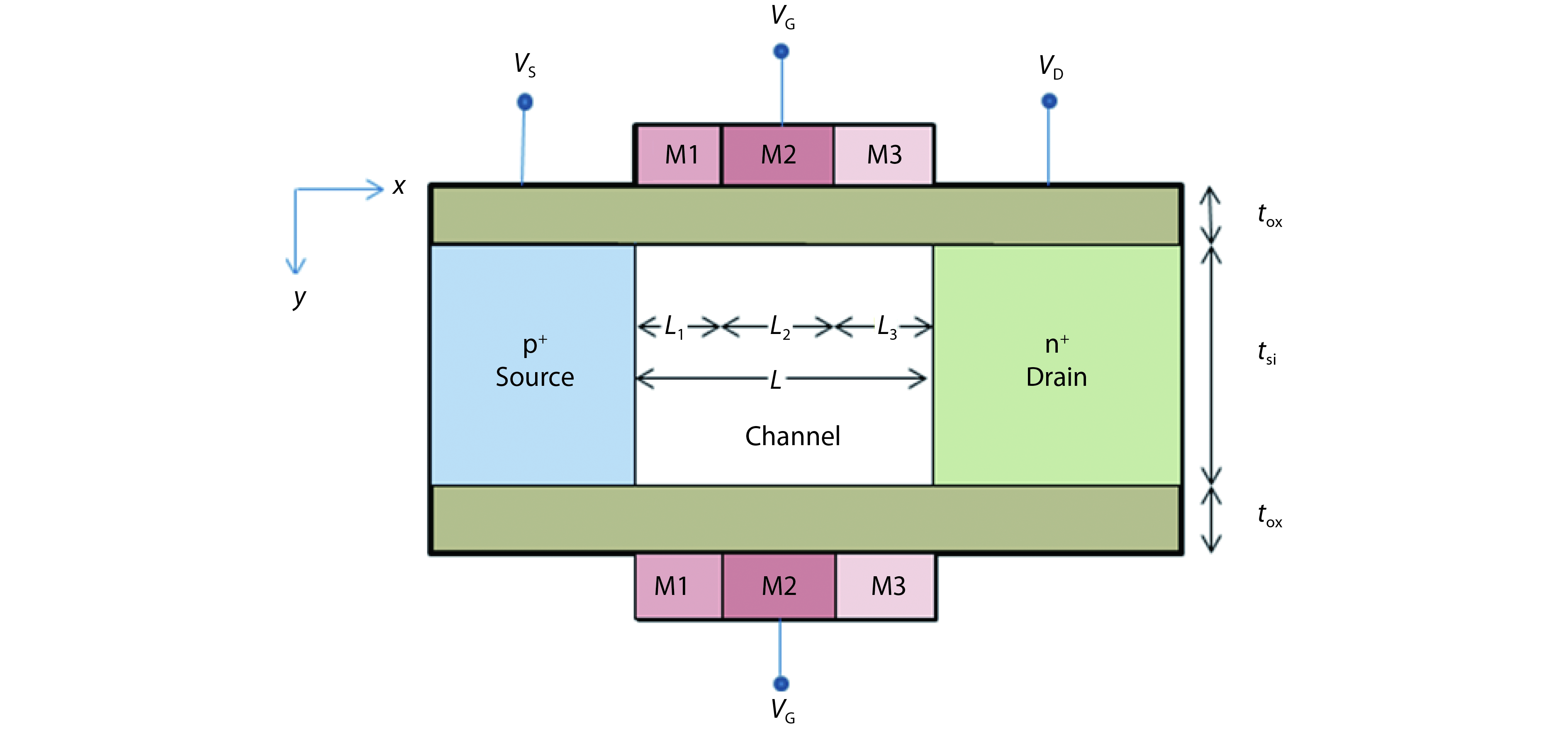
Fig. 1.
(Color online) Schematic diagram of triple metal double-gate TFET (n-type).
ARTICLES
Corresponding author: C. Usha, usha.chintu.dec14@gmail.com
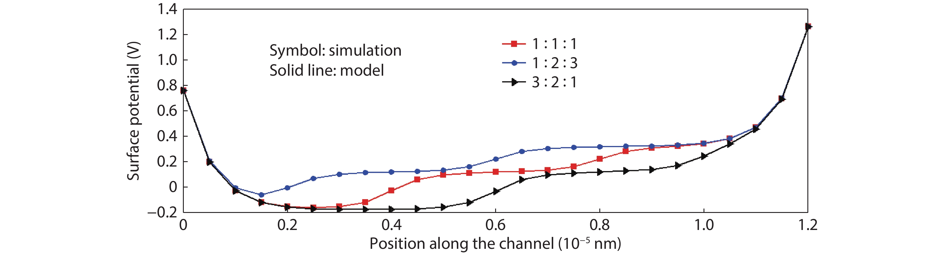
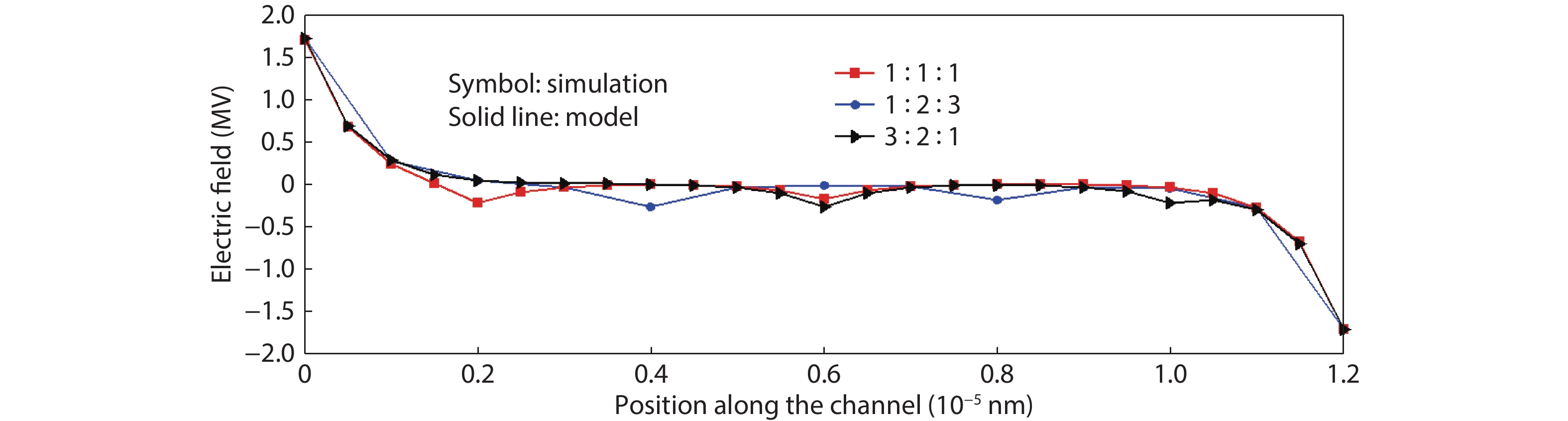
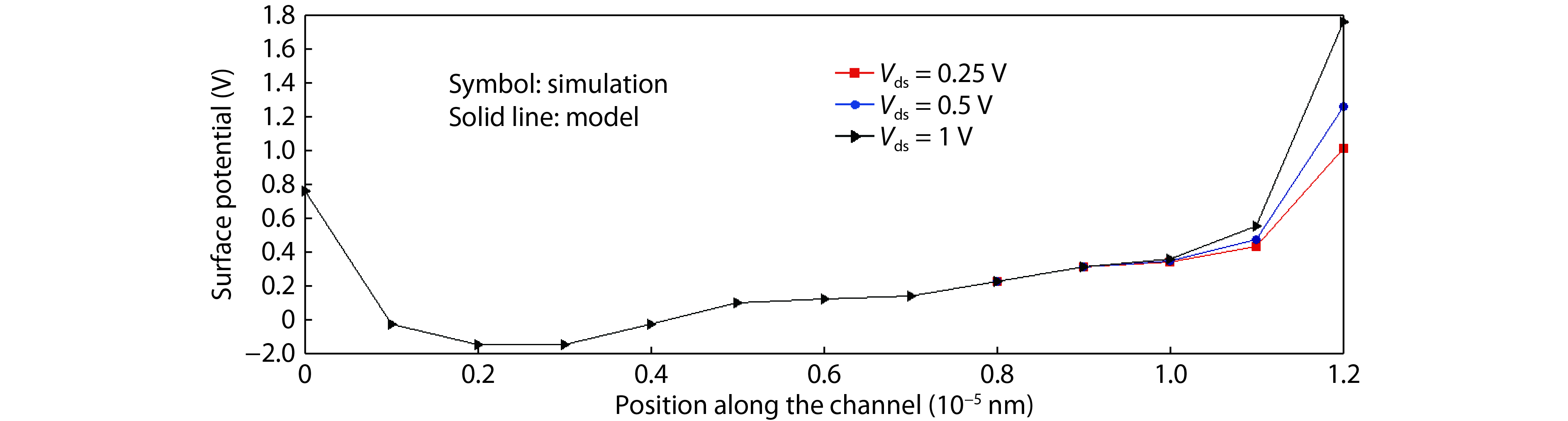
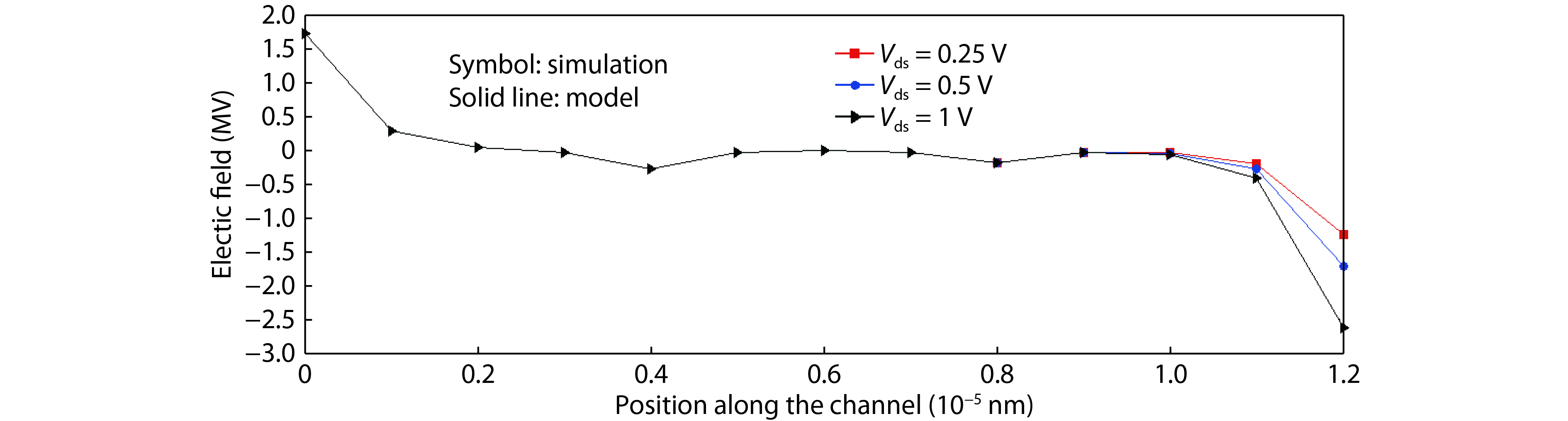
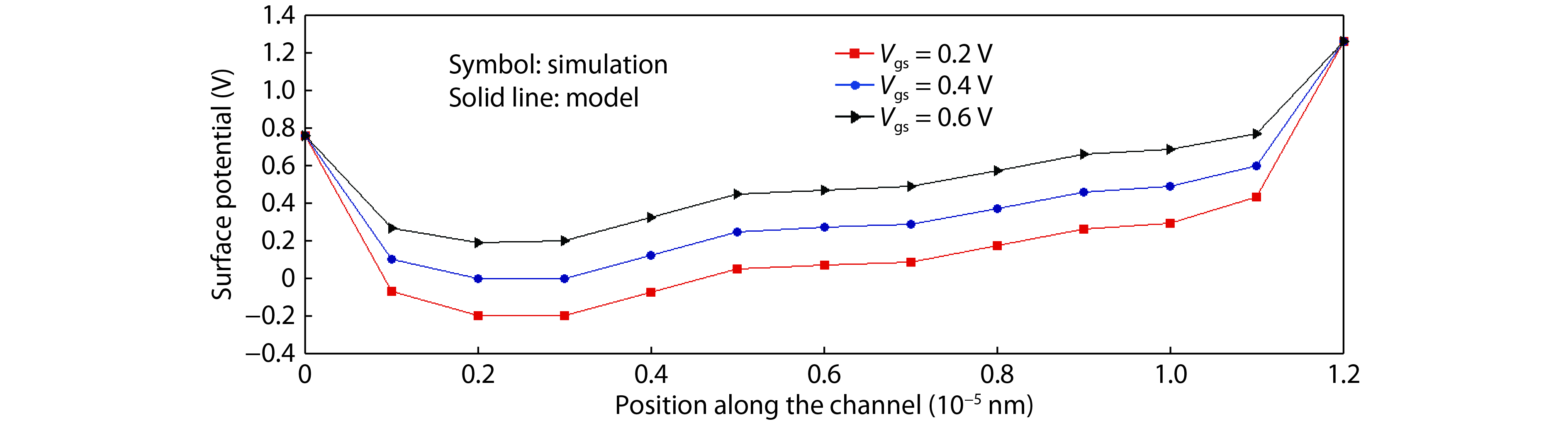
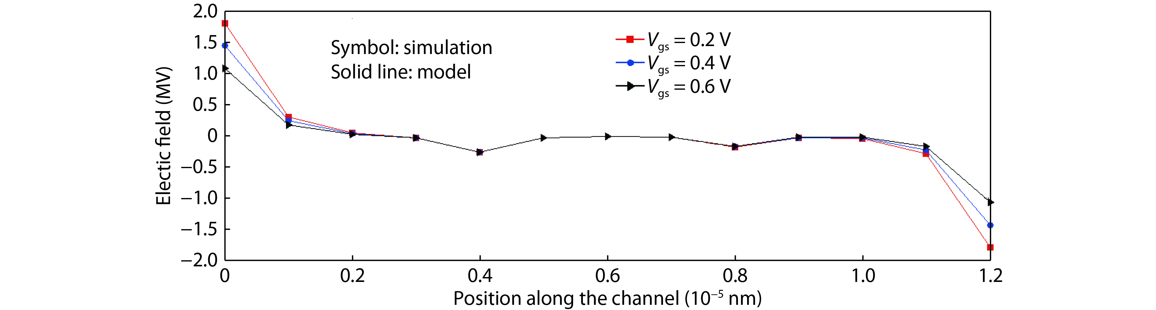
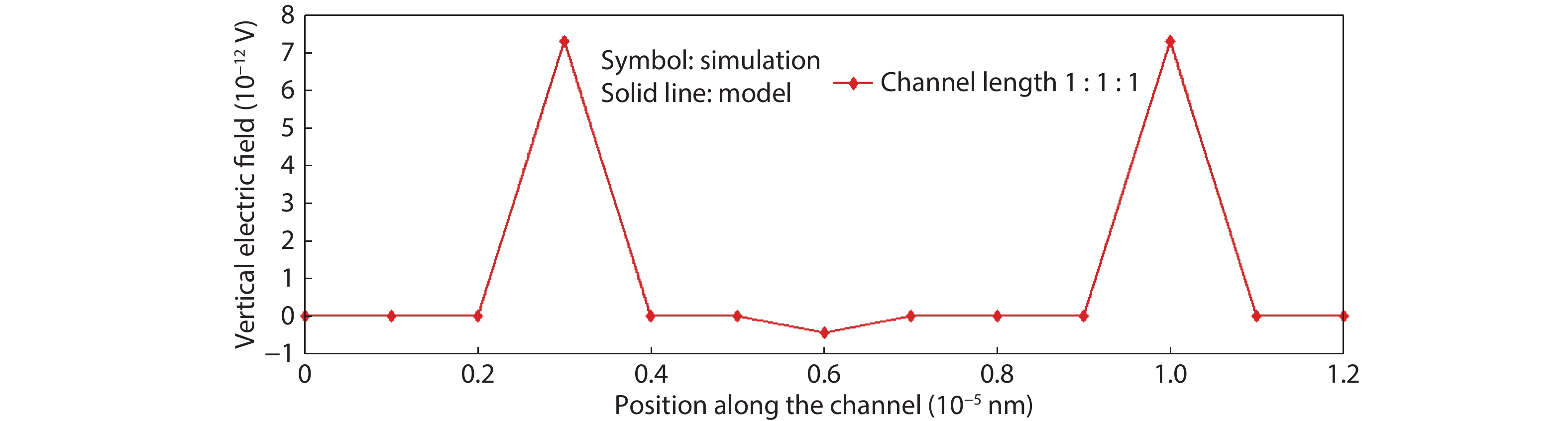
Abstract: This paper presents a compact two-dimensional analytical device model of surface potential, in addition to electric field of triple-material double-gate (TMDG) tunnel FET. The TMDG TFET device model is developed using a parabolic approximation method in the channel depletion space and a boundary state of affairs across the drain and source. The TMDG TFET device is used to analyze the electrical performance of the TMDG structure in terms of changes in potential voltage, lateral and vertical electric field. Because the TMDG TFET has a simple compact structure, the surface potential is computationally efficient and, therefore, may be utilized to analyze and characterize the gate-controlled devices. Furthermore, using Kane's model, the current across the drain can be modeled. The graph results achieved from this device model are close to the data collected from the technology computer aided design (TCAD) simulation.
Key words: triple-material double-gate TFET, surface potential, lateral and vertical electric field, drain current, TCAD simulation
| [1] |
Toh E H, Wang G H, Samudra G, et al. Device physics and design of germanium tunneling field-effect transistor with source and drain engineering for low power and high performance applications. J Appl Phys, 2008, 103, 104504 doi: 10.1063/1.2924413
|
| [2] |
Koswatta S O, Lundstrom M S, Nikonov S E, et al. Performance comparison between p–i–n tunneling transistors and conventional MOSFETs. IEEE Trans Electron Devices, 2009, 56, 456 doi: 10.1109/TED.2008.2011934
|
| [3] |
Seabaugh A C, Zhang Q. Low-voltage tunnel transistors for beyond CMOS logic. Proc IEEE, 2010, 98, 2095 doi: 10.1109/JPROC.2010.2070470
|
| [4] |
Saurabh S, Kumar M J. Novel attributes of a dual material gate nanoscale tunnel field-effect transistor. IEEE Trans Electron Devices, 2011, 58, 404 doi: 10.1109/TED.2010.2093142
|
| [5] |
Gnani E, Gnudi A, Reggiani S, et al. Drain-conductance optimization in nanowire TFETs by means of a physics-based analytical model. Solid-State Electron, 2013, 84, 96 doi: 10.1016/j.sse.2013.02.012
|
| [6] |
Boucart K, Ionescu A M. A new definition of threshold voltage in tunnel FETs. Solid State Electron, 2008, 52, 1318 doi: 10.1016/j.sse.2008.04.003
|
| [7] |
Vandenberghe W, Verhulst A, Greseneken G, et al. Analytical model for tunnel field- effect transistor. Proc MELECON, 2008, 923
|
| [8] |
Mojunder N N, Roy K. Band-to-Band tunneling ballistic low-power digital circuits and memories. IEEE Trans Electron Devices, 2009, 56, 2193 doi: 10.1109/TED.2009.2028394
|
| [9] |
Vandenberghe W, Verhulst A, Greseneken G, et al. Analytical model for point and line tunneling in a tunnel field-effect transistor. Proc Int Conf SISPAD, 2008, 137
|
| [10] |
Bardon M G, Neves H P, Puerd R, et al. Pseudo-two dimensional model for double gate tunnel FETs considering the junctions depletion regions. IEEE Trans Electron Devices, 2010, 57, 827 doi: 10.1109/TED.2010.2040661
|
| [11] |
Liu L, Mohata D, Datta S. Scaling length theory of double-gate interband tunnel field-effect transistors. IEEE Trans Electron Devices, 2012, 59, 902 doi: 10.1109/TED.2012.2183875
|
| [12] |
Lee M J, Choi W Y. Analytical model of single-gate silicon on insulator tunneling field effect tansistors (TFETs). Solid State Electron, 2011, 63, 110 doi: 10.1016/j.sse.2011.05.008
|
| [13] |
Zhang L, Lin X, He J, et al. Analytical charge model for double gate tunnel FETs. IEEE Trans Electron Devices, 2012, 59, 3217 doi: 10.1109/TED.2012.2217145
|
| [14] |
Pan A, Chui C O. A quasi-analytical model for double-gate tunneling field effect transistors. IEEE Trans Electron Devices, 2012, 33, 1468 doi: 10.1109/LED.2012.2208933
|
| [15] |
Bhushan B, Nayak K, Rao V R. DC compact model for SOI tunnel field-effect tansistors. IEEE Trans Electron Devices, 2012, 59, 2635 doi: 10.1109/TED.2012.2209180
|
| [16] |
Verhulst A S, Leoneli D, Rooyackers R, et al. Drain voltage dependent analytical model of tunnel field-effect transistor. J Appl Phys, 2011, 110, 024510 doi: 10.1063/1.3609064
|
| [17] |
Dobrovolsky V, Sizov F. Analytical model of the thin-film silicon-on-insulator tunneling field effect transistor. J App Phys, 2011, 110, 114513 doi: 10.1063/1.3660795
|
| [18] |
Wan J, Royer C L, Zaslavsky A, et al. A tunneling field effect transistor model conbining interband tunneling with channel transport. J Appl Phys, 2011, 110, 104503 doi: 10.1063/1.3658871
|
| [19] |
Vishnoi R, Kumar M J. Compact analytical model of dual material gate tunneling field-effect transistor using interband tunneling and channel transport. IEEE Trans Electron Devices, 2014, 61, 1936 doi: 10.1109/TED.2014.2315294
|
| [20] |
Samuel T S A, Balamurugan N B. An analytical modeling and simulation of dual material double gate tunnel field effect transistor for low power applications. J. Elect Eng Technol, 2014, 9, 247 doi: 10.5370/JEET.2014.9.1.247
|
| [21] |
Vishnoi R, Kumar M J. 2-D analytical model for the threshold voltage of a tunneling FET with localized charges. IEEE Trans Electron Devices, 2014, 61, 3054 doi: 10.1109/TED.2014.2332039
|
| [22] |
Pandey P, Vishnoi R, Kumar M J. A full-range dual material gate tunnel field effect transistor drain current model considering both source and drain depletion region band-to-band tunneling. J Comput Electron, 2014, 14, 280 doi: 10.1007/s10825-014-0649-x
|
| [23] |
Zhang L, Chan M. SPICE modelling of double-gate tunnel-FETs including channel transports. IEEE Trans Electron Devices, 2014, 61, 300 doi: 10.1109/TED.2013.2295237
|
| [24] |
Vishnoi R, Kumar M J. An accurate compact analytical model for the drain current of a TFET from subthreshold to strong inversion. IEEE Trans Electron Devices, 2015, 62, 478 doi: 10.1109/TED.2014.2381560
|
| [25] |
Dash S, Mishra G P. A two-dimensional analytical cylindrical gate tunnel FET (CG-TFET) model: Impact of shortest tunneling distance. Adv Natural Sci, Nanosci Nanotechnol, 2015, 6, 035005 doi: 10.1088/2043-6262/6/3/035005
|
| [26] |
Bagga N, Sarkar S K. An analytical model for tunnel barrier modulation in triple metal double gate TFET. IEEE Trans Electron Devices, 2015, 62, 2136 doi: 10.1109/TED.2015.2434276
|
| [27] |
Dash S, Mishra G P. A new analytical threshold voltage model of cylindrical gate tunnel FET (CG-TFET). Superlattices Microstruct, 2015, 86, 211 doi: 10.1016/j.spmi.2015.07.049
|
| [28] |
Noor S L, Safa S, Khan M Z R. Dual-material double-gate tunnel FET: Gate threshold voltage modeling and extraction. J Comput Electron, 2016, 15, 763 doi: 10.1007/s10825-016-0816-3
|


Article views: 4326 Times PDF downloads: 78 Times Cited by: 0 Times
Received: 07 February 2019 Revised: 15 May 2019 Online: Accepted Manuscript: 13 August 2019Uncorrected proof: 13 August 2019Published: 09 December 2019
| Citation: |
C. Usha, P. Vimala. A compact two-dimensional analytical model of the electrical characteristics of a triple-material double-gate tunneling FET structure[J]. Journal of Semiconductors, 2019, 40(12): 122901. doi: 10.1088/1674-4926/40/12/122901
****
C Usha, P Vimala, A compact two-dimensional analytical model of the electrical characteristics of a triple-material double-gate tunneling FET structure[J]. J. Semicond., 2019, 40(12): 122901. doi: 10.1088/1674-4926/40/12/122901.

|
| [1] |
Toh E H, Wang G H, Samudra G, et al. Device physics and design of germanium tunneling field-effect transistor with source and drain engineering for low power and high performance applications. J Appl Phys, 2008, 103, 104504 doi: 10.1063/1.2924413
|
| [2] |
Koswatta S O, Lundstrom M S, Nikonov S E, et al. Performance comparison between p–i–n tunneling transistors and conventional MOSFETs. IEEE Trans Electron Devices, 2009, 56, 456 doi: 10.1109/TED.2008.2011934
|
| [3] |
Seabaugh A C, Zhang Q. Low-voltage tunnel transistors for beyond CMOS logic. Proc IEEE, 2010, 98, 2095 doi: 10.1109/JPROC.2010.2070470
|
| [4] |
Saurabh S, Kumar M J. Novel attributes of a dual material gate nanoscale tunnel field-effect transistor. IEEE Trans Electron Devices, 2011, 58, 404 doi: 10.1109/TED.2010.2093142
|
| [5] |
Gnani E, Gnudi A, Reggiani S, et al. Drain-conductance optimization in nanowire TFETs by means of a physics-based analytical model. Solid-State Electron, 2013, 84, 96 doi: 10.1016/j.sse.2013.02.012
|
| [6] |
Boucart K, Ionescu A M. A new definition of threshold voltage in tunnel FETs. Solid State Electron, 2008, 52, 1318 doi: 10.1016/j.sse.2008.04.003
|
| [7] |
Vandenberghe W, Verhulst A, Greseneken G, et al. Analytical model for tunnel field- effect transistor. Proc MELECON, 2008, 923
|
| [8] |
Mojunder N N, Roy K. Band-to-Band tunneling ballistic low-power digital circuits and memories. IEEE Trans Electron Devices, 2009, 56, 2193 doi: 10.1109/TED.2009.2028394
|
| [9] |
Vandenberghe W, Verhulst A, Greseneken G, et al. Analytical model for point and line tunneling in a tunnel field-effect transistor. Proc Int Conf SISPAD, 2008, 137
|
| [10] |
Bardon M G, Neves H P, Puerd R, et al. Pseudo-two dimensional model for double gate tunnel FETs considering the junctions depletion regions. IEEE Trans Electron Devices, 2010, 57, 827 doi: 10.1109/TED.2010.2040661
|
| [11] |
Liu L, Mohata D, Datta S. Scaling length theory of double-gate interband tunnel field-effect transistors. IEEE Trans Electron Devices, 2012, 59, 902 doi: 10.1109/TED.2012.2183875
|
| [12] |
Lee M J, Choi W Y. Analytical model of single-gate silicon on insulator tunneling field effect tansistors (TFETs). Solid State Electron, 2011, 63, 110 doi: 10.1016/j.sse.2011.05.008
|
| [13] |
Zhang L, Lin X, He J, et al. Analytical charge model for double gate tunnel FETs. IEEE Trans Electron Devices, 2012, 59, 3217 doi: 10.1109/TED.2012.2217145
|
| [14] |
Pan A, Chui C O. A quasi-analytical model for double-gate tunneling field effect transistors. IEEE Trans Electron Devices, 2012, 33, 1468 doi: 10.1109/LED.2012.2208933
|
| [15] |
Bhushan B, Nayak K, Rao V R. DC compact model for SOI tunnel field-effect tansistors. IEEE Trans Electron Devices, 2012, 59, 2635 doi: 10.1109/TED.2012.2209180
|
| [16] |
Verhulst A S, Leoneli D, Rooyackers R, et al. Drain voltage dependent analytical model of tunnel field-effect transistor. J Appl Phys, 2011, 110, 024510 doi: 10.1063/1.3609064
|
| [17] |
Dobrovolsky V, Sizov F. Analytical model of the thin-film silicon-on-insulator tunneling field effect transistor. J App Phys, 2011, 110, 114513 doi: 10.1063/1.3660795
|
| [18] |
Wan J, Royer C L, Zaslavsky A, et al. A tunneling field effect transistor model conbining interband tunneling with channel transport. J Appl Phys, 2011, 110, 104503 doi: 10.1063/1.3658871
|
| [19] |
Vishnoi R, Kumar M J. Compact analytical model of dual material gate tunneling field-effect transistor using interband tunneling and channel transport. IEEE Trans Electron Devices, 2014, 61, 1936 doi: 10.1109/TED.2014.2315294
|
| [20] |
Samuel T S A, Balamurugan N B. An analytical modeling and simulation of dual material double gate tunnel field effect transistor for low power applications. J. Elect Eng Technol, 2014, 9, 247 doi: 10.5370/JEET.2014.9.1.247
|
| [21] |
Vishnoi R, Kumar M J. 2-D analytical model for the threshold voltage of a tunneling FET with localized charges. IEEE Trans Electron Devices, 2014, 61, 3054 doi: 10.1109/TED.2014.2332039
|
| [22] |
Pandey P, Vishnoi R, Kumar M J. A full-range dual material gate tunnel field effect transistor drain current model considering both source and drain depletion region band-to-band tunneling. J Comput Electron, 2014, 14, 280 doi: 10.1007/s10825-014-0649-x
|
| [23] |
Zhang L, Chan M. SPICE modelling of double-gate tunnel-FETs including channel transports. IEEE Trans Electron Devices, 2014, 61, 300 doi: 10.1109/TED.2013.2295237
|
| [24] |
Vishnoi R, Kumar M J. An accurate compact analytical model for the drain current of a TFET from subthreshold to strong inversion. IEEE Trans Electron Devices, 2015, 62, 478 doi: 10.1109/TED.2014.2381560
|
| [25] |
Dash S, Mishra G P. A two-dimensional analytical cylindrical gate tunnel FET (CG-TFET) model: Impact of shortest tunneling distance. Adv Natural Sci, Nanosci Nanotechnol, 2015, 6, 035005 doi: 10.1088/2043-6262/6/3/035005
|
| [26] |
Bagga N, Sarkar S K. An analytical model for tunnel barrier modulation in triple metal double gate TFET. IEEE Trans Electron Devices, 2015, 62, 2136 doi: 10.1109/TED.2015.2434276
|
| [27] |
Dash S, Mishra G P. A new analytical threshold voltage model of cylindrical gate tunnel FET (CG-TFET). Superlattices Microstruct, 2015, 86, 211 doi: 10.1016/j.spmi.2015.07.049
|
| [28] |
Noor S L, Safa S, Khan M Z R. Dual-material double-gate tunnel FET: Gate threshold voltage modeling and extraction. J Comput Electron, 2016, 15, 763 doi: 10.1007/s10825-016-0816-3
|

 WeChat ID
Journal of Semiconductors © 2017 All Rights Reserved 京ICP备05085259号-2

 DownLoad:

