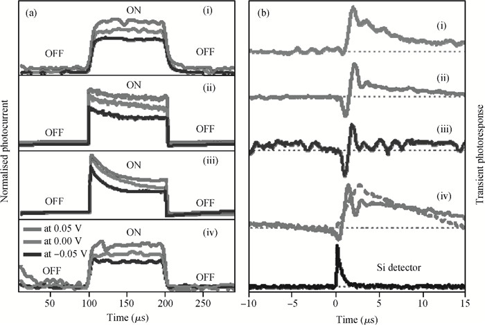
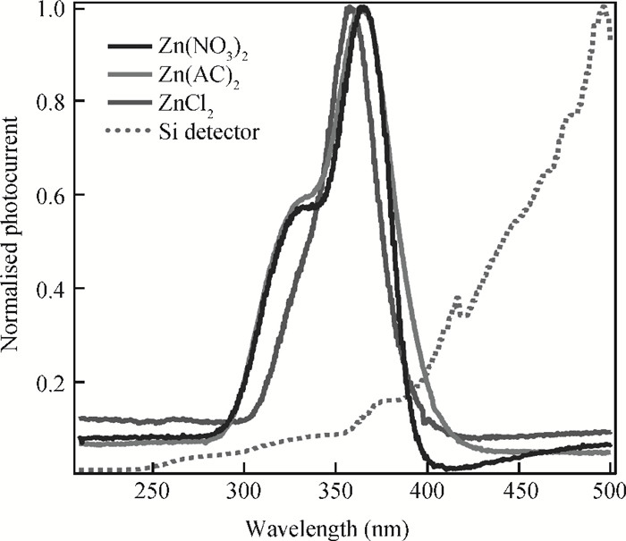
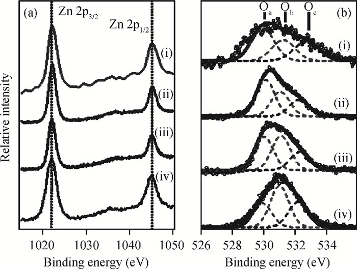
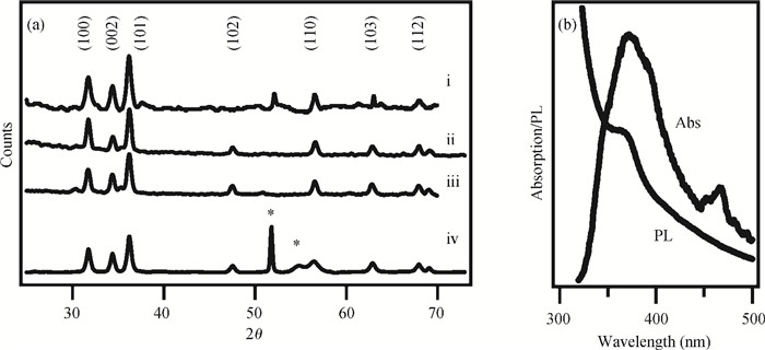
Processing math: 100%
J. Semicond. > 2013, Volume 34 > Issue 3 > 033001

SEMICONDUCTOR MATERIALS

Photoconductivity and surface chemical analysis of ZnO thin films deposited by solution-processing techniques for nano and microstructure fabrication

V.K. Dwivedi1, 2, P. Srivastava2 and G. Vijaya Prakash1

+ Author Affiliations

 Corresponding author: G. Vijaya Prakash, prakash@physics.iitd.ac.in

DOI: 10.1088/1674-4926/34/3/033001

PDF

Abstract: The fabrication of zinc oxide (ZnO) from inexpensive solution-processing techniques, namely, electrochemical deposition and electrospinning were explored on various conducting and mesoporous semiconducting surfaces. Optimised conditions were derived for template-and self-assisted nano/micro structures and composites. ZnO thin films were annealed at a fixed temperature under ambient conditions and characterised using physical and optical techniques. The photocurrent response in the UV region shows a fast rise and double decay behaviour with a fast component followed by a slow oscillatory decay. Photocurrent results were correlated with surface chemical analysis from X-ray photoelectron spectroscopy. Various characterisation details reveal the importance of fabrication parameter optimisation for useful low-cost optoelectronic applications.

Key words: zinc oxideelectrochemical depositionsurface analysisX-ray photoelectron spectroscopyphotocurrent responseoptoelectronic applications

ZnO has attracted increasing attention as a potential material for optoelectronic devices such as low threshold blue/UV lasers, solar cells, LEDs, sensors, display devices and photodetectors[1-3]. In recent years, various attempts were made to fabricate nano/mesa-scaled ZnO for further enhancing opto/electrical performance. While many top-down fabrication approaches were followed, solution-based techniques turned out to be the most efficient and low-cost for the production of high quality nano and micro structured ZnO thin films[4, 5]. Electrochemical deposition is a true bottom-up technique, with the convenience of completely filling the interstitial spaces of templates, such as polymer microsphere templates, liquid crystal templates and porous (such as porous alumina) templates, from metal to semiconductor varieties[6, 7]. Similarly, electrospinning has been widely recognised as an electro-hydrodynamic method to produce nano to micro sized fibers from solutions containing the desired materials[8, 9]. However, the optoelectronic properties of ZnO are critically affected by the preparation conditions such as the fabrication method, types of substrates, thickness and annealing conditions. Therefore, it is necessary to optimise the fabrication conditions of the aforementioned techniques for desired applications.

The direct electrochemical deposition of semiconductors, such as ZnO, on a silicon substrate is difficult due to conductivity issues as well as a large mismatch in thermal expansion coefficients and the high reactivity of silicon toward oxygen[10-14]. Porous silicon (PS) has been established as the most fascinating material for diverse optoelectronic applications[15-17], especially for photonic composites where the nano sized pores can be filled with different materials using simple solution-processing techniques[18, 19].

In this paper, we have explored various solution-processing techniques to produce ZnO thin films on conducting (ITO) and silicon substrates along with ZnO-porous silicon composite films. All these samples obtained from different methods and chemical recipes were annealed under fixed ambient conditions and characterised by scanning electron microscopy (SEM), X-ray diffraction (XRD), X-ray photoelectron spectroscopy (XPS), optical absorption, photoluminescence (PL) and ultraviolet photocurrent response. All films obtained from various chemical recipes were essentially in the form of Zn(OH)2 after preparation, and to obtain ZnO, the samples were annealed at 400 ℃ for 12 h under ambient conditions. Various characterisations reveal that the fabrication conditions and intrinsic defects of ZnO play a vital role in optoelectronic performance.

ZnO nano and micro structures were fabricated from template-assisted electrochemical deposition, and electro-spinning methods. In electrochemical deposition, two aqueous electrolyte solutions were employed, namely, (1) 0.1M Zn(NO3)2 and (2) a mixture of 5 mM ZnCl2 with 0.1 M KCl on both the ITO and silicon substrates using a potentiostatic three-electrode method[7, 20, 21].

Similarly porous silicon is used as a template to fabricate nano-scaled ZnO. PS with different porosities were made by electrochemical etching using a p(100) type silicon wafer, as detailed in Ref.[18]. ZnO-porous silicon composites were prepared by electrochemical deposition of ZnO into the pores of PS, from a ZnCl2 electrolyte as mentioned above. In this paper, we have shown the results of the ZnO-PS nanocomposites, where ZnO is electrodeposited into the pores of the 70% porosity PS of thickness 150 nm on the silicon substrate. To ensure complete wetting of the pores, the PS was soaked in the electrolyte for about 1 h.

All films obtained from various chemical recipes were essentially in the form of Zn(OH)2 and to obtain ZnO, the samples were annealed at 400 ℃ for 12 h under ambient conditions.

The crystalline phases of the thin films were identified by an X-ray diffraction (XRD) technique using a CuKα source (λ = 1.54 Å. The chemical state of the different elements present in the thin films was analyzed by X-ray photoelectron spectroscopy (XPS) using a Mg Kα source (hv = 1253.6 eV). Prior to these measurements, Argon etching for a 2 min duration was performed to remove a few atomic layers of the surface to avoid any surface contamination. The binding energy of the XPS spectra has been calibrated by taking the C1s peak (284.6 eV) as a reference. Steady-state and transient photocurrent response studies of ZnO films were investigated by the three-electrode wet-contact method[22]. A commercial Si detector (UDT model No. 260) was used as a photocurrent response reference. For photocurrent measurements, a wet-contact three-electrode method was used wherein an aqueous solution of 0.1 M KI acts as an electrolyte. A saturated Calomel electrode, a platinum mesh and a ZnO film deposited on substrates were used as the reference, counter and working electrodes respectively. A nitrogen laser with 2 mW power (337 nm wavelength, 100 Hz pulsed frequency and 5 ns pulse width) was used as a UV irradiation and photocurrent was monitored by computer controlled potentiostat and a digital oscilloscope. To measure the photocurrent in the spectral domain, Xenon (75 W) attached to a monochromator is used as a photoexcitation source. PL measurements were carried out using a monochromator and a PMT, using a nitrogen laser (337 nm) as an excitation source.

The obtained ZnO thin films from various solution processing methods show considerable variation in structural, optical and optoelectronic properties on deposition parameters and conditions[7]. Since the annealing condition for all the films was same (400 ℃ for 12 h in air), in the present study the structural and optical properties of various films are compared and analyzed. As shown in Fig. 1, the XRD patterns were recorded for all annealed ZnO thin films obtained from (1) electrodeposition from ZnCl2 onto a silicon substrate, (2) electrodeposition from Zn(NO3)2 solutions onto an ITO substrate, (3) electro-spinned ZnO from a Zn(Ac)2 solution onto an ITO substrate, and (4) a ZnO-PS nanocomposite. Asterisks (*) indicate the XRD peaks of silicon. All the films were showing strong XRD peaks of wurtzite crystalline structure, with traces of substrate (Si) related diffraction peaks.

Figure  1.  (a) XRD patterns of ZnO (Ⅰ) electrodeposited from ZnCl2 and (Ⅱ) electrodeposited from Zn(NO3)2 solutions, (Ⅲ) electro-spinned ZnO from Zn(Ac)2 solution and (Ⅳ) ZnO-PS nanocomposite. The asterisk (*) indicates XRD peaks of silicon. XRD patterns are shifted along the y-axis for clarity. (b) Absorption and photoluminescence spectra of electro-spinned ZnO fibers.

In our previous communication[7], we have shown photoluminescence (PL) studies and reported that the ZnO fabricated from various electrochemical deposition parameters show different PL: exciton (in the UV region) related PL as well as deep level defects related PL (in blue-green region). In particular, the deep level defects were attributed to the oxygen vacancy defects and interstitial Zn ions. While ZnO obtained from electro-deposition shows both exciton as well as defect related PL, the ZnO obtained from electro-spinning shows dominant excitonic related features in both absorption as well as PL, indicating the minimum influence of defects (Fig. 1(b)).

In brief, the ZnO obtained from different solution processing methods shows widely different PL properties. In order to establish the ZnO as a multi-functional material, it is worthwhile to study and understand the photocurrent response of these samples, especially the generation and recombination of photo-carriers. Therefore, such systematic studies were performed and presented as follows.

Steady-state and transient photocurrent measurements were performed on all ZnO films made from different solution processing techniques. Here the ZnO films were exposed to a UV laser (2 mW, 337 nm) and the photocurrent was monitored using the wet electrode method. Figure 2(a) shows the normalised photocurrent response, when the illuminated light was switched ON and OFF at different bias conditions. The data represents the ZnO thin films obtained from (1) electrochemical deposition from ZnCl2, (2) electrochemical deposition from Zn(NO3)2 solutions, (3) electrospinned film from a Zn(Ac)2 solution and (4) a ZnO-PS nanocomposite. As seen, the photocurrent varies linearly with the increase in the bias voltage. While all films show more or less similar responses, the photocurrent efficiencies measured under similar conditions are different. Here, the photocurrent efficiency is defined as QE =(IphotoIdark)/Idark, where the Idark and Iphoto are the photocurrents when the light is OFF and ON, respectively. The QE for ZnO obtained from electrospinned film from Zn(Ac)2 solution is 41 whereas for ZnO-PS the nanocomposite is only 5.

Figure  2.  (a) Normalised photocurrent ON-OFF response of ZnO films prepared from various methods. (b) Transient photocurrent response of ZnO deposited from various methods, the commercial Si detector response is shown as a reference. Labels i, ii, iii and iv represent the same as Fig. 1(a). The transient response for pure PS, overlapping ZnO-PS (dashed curve in Fig. 2(b) (iv)), is shown for comparison. All the graphs are in Fig. (b) are shifted along the y-axis for clarity.

To study the transient photocurrent behaviour, the resultant photocurrent response obtained from the excitation of a nanosecond UV laser (337 nm, 5 ns, 100 Hz) was monitored through a digital oscilloscope using a commercial silicon detector as a photocurrent response reference (Fig. 2(b)). Essentially all films show a fast photocurrent rise followed by an oscillatory decay. The photocurrent decay is composed of two components: a fast fall followed by slow fall of an oscillatory nature. The transient response is fitted using a bi-exponential function, I=I0+Aexp(t/τ1)+Bexp(t/τ2). Both the rise and fall time values obtained from such fittings are given in Table 1. A similar fast decay followed by oscillatory decay behaviour has been reported previously for ZnO from RF sputtering[23, 24], ZnO alloyed with MgO from pulsed laser deposition[25], and epitaxial ZnO obtained from MOCVD[26]. The present decay times were compared with these reported values in Table 1.

Table  1.  Photocurrent response rise time, fall and slow fall times and efficiencies (QE) and estimated percentage of oxygen vacancies from the XPS analysis of ZnO fabricated from various methods. The data of ZnO prepared from various other methods reported in the literature are also given for comparison.
DownLoad: CSV  | Show Table

In general, the order of rise and initial fast fall times of various ZnO shows the following trend: ZnO-PS nanocomposite > ZnO from Zn(Ac)2 > ZnO from Zn(NO3)2 > ZnO from ZnCl2. It is interesting to compare these results with the QE values obtained earlier, where the QE value of ZnO from Zn(Ac)2 is the highest and ZnO-PS is the lowest.

The photoconductivity phenomena in ZnO are generally related to either surface or to bulk related processes. The surface related process are due to adsorption and desorption of the chemisorbed oxygen on the surface of ZnO. Upon photo excitation, using light energy greater than the band gap of the material, three types of photocurrent processes are expected: (1) chemisorption of O2, (2) desorption of O2 and (3) recombination of the electron-hole pair. The dominant process among these three defines the resultant nature of photocurrent. The holes eventually react with chemisorbed oxygen and release O2 (O2 + h+ O2 (g) (desorption)) leaving behind electrons, which take part in photocurrent. Further, oxygen molecules are chemisorbed on the surface of ZnO and capture the electrons as O2(g) + e O2 (adsorbed species)[27, 28]. Therefore, the transient photocurrent response rise time is due to the desorption of O2. Whereas, the photocurrent fast fall is due to the transit time taken by the carriers, which is inversely proportional to the electron mobility and bias voltage[22]. The oscillatory slow decay phenomenon is the result of persistent photoconductivity effects attributed to the presence of oxygen-related hole-trap states at the surface, which prevent charge-carrier recombination and prolongs the photocarrier lifetime. Similar behaviour has been observed for the ZnO fabricated from various other methods[23-25]. While the ZnO grown from various aforementioned methods shows a good crystalline quality, the origin of oxygen defects on the surfaces could be from both deposition conditions as well as annealing in an air atmosphere. However, in the present case, though solution processing recipes are different, the obtained ZnO may be compared since the annealing conditions for all the ZnO films are the same. Hence, these results broadly suggest that the photocurrent response of ZnO could be related to its structural and surface properties, essentially to the process induced intrinsic defects of ZnO[29, 30]. Figure 3 shows the wavelength (200-500 nm) dependent photocurrent characteristics of ZnO thin films fabricated from various precursors. The spectral responsivity shows a distinct broad peak centred at about 360 nm, which correspond to the band gap of ZnO[7, 27, 32].

Figure  3.  Wavelength dependent photocurrent response of ZnO electrodeposited thin films obtained from Zn(NO3)2 Zn(Ac)2 and ZnCl2 solutions. The bias voltage is set at 0 V. The spectral photocurrent response of the commercial Si detector is also included for comparison.

To get more information about the surface composition and the intrinsic defects (Zn interstitials and oxygen vacancies), X-ray photoelectron spectroscopy (XPS) measurements were carried out on all these samples. Figure 4(a) shows the XPS spectra of Zn2p core levels, where the peaks at 1021.8 and at 1044.9 eV correspond to Zn2p3/2 and Zn2p1/2 core levels respectively which confirm the presence of Zn in a +2 state in the matrix. Figure 4(b) shows that the O1s peak is asymmetric and can be fitted by three nearly Gaussian curves centred at 529.9, 531 and 532.2 eV. The peak at 532.2 eV (Oc) is usually attributed to the presence of loosely bound oxygen on the surface of the ZnO, belonging to a specific species, e.g., adsorbed H2O or adsorbed O2. The medium binding energy component 531(Ob) is associated with O2 ions in oxygen deficient regions (oxygen vacancies) within the matrix of ZnO. The component on the low binding energy side of the O1s spectrum at 529.9 eV (Oa) is due to the oxygen in the ZnO matrix[31, 32]. The oxygen vacancies estimated from the XPS results follow the trend: ZnO-PS nanocomposite > ZnO from Zn(Ac)2 > ZnO from Zn(NO3)2 > ZnO from ZnCl2. These results follow the same trend as the photocurrent response results. Therefore, the photocurrent response of ZnO could be broadly related to the oxygen vacancies, especially as the rise time and fast decay of photocurrent appears to be inversely dependent on the oxygen vacancies. Such fast photocurrent response times are much more favourable for the Schottky type of UV detectors[26]. In future, it would be worthwhile extending the study to further investigate the effect of annealing conditions and surface morphology of various nanostrucutured films.

Figure  4.  (Colour online) XPS spectra of (a) Zn2p core levels and (b) O1s core level with Gaussian fits (dotted lines) for Oa, Ob and Oc. Labels i, ii, iii and iv represent the same as Fig. 1(a). Spectra are shifted along the Y-axis for clarity.

Several solution-processing inexpensive deposition techniques, such as template-assisted electrochemical deposition and electrospinning have been explored and optimised conditions were derived to obtain high-quality wurtzite crystalline ZnO. Furthermore, the optical and physical properties of thin films obtained from these deposition techniques were investigated. While all the samples show a wurtzite crystalline structure, their optical properties are significantly different. These films show a typical fast photocurrent response component of rise time about 1 μs and fall time of 2 μs with persistent photoconductive behaviour. XPS surface analysis observations suggest a possible correlation between oxygen related defects to the photocurrent measurements. The low-cost methodology and multi-functional optical properties (fast photocurrent response and exciton PL) are useful for low-cost UV optoelectronic devices.

Acknowledgements: This work was partly supported by the UK-India Education and Research Initiative (UKIERI) and the High-Impact Research Scheme of IIT Delhi. The authors thank Dr. Santanu Ghosh and Mr. Sarabpreet Singh of IIT Delhi for their help. One of the authors (V.K.D.) is thankful to the University Grants Commission (UGC), New Delhi, India, for financial assistance.


[1]
Tan S T, Chen B J, Sun X W, et al. Blueshift of optical band gap in ZnO thin films grown by metal-organic chemical-vapor deposition. J Appl Phys, 2005, 98(1):013505 doi: 10.1063/1.1940137
[2]
Park J W, Kim J K, Suh K Y. Fabrication of zinc oxide nanostructures using solvent-assisted capillary lithography. Nanotechnology, 2006, 17(10):2631 doi: 10.1088/0957-4484/17/10/031
[3]
Park J H, Jang S J, Kim S S, et al. Growth and characterization of single crystal ZnO thin films using inductively coupled plasma metal organic chemical vapor deposition. Appl Phys Lett, 2006, 89(12):121108 doi: 10.1063/1.2356075
[4]
Tian Z R, Voigt J A, Liu J, et al. Complex and oriented ZnO nanostructures. Nat Mater, 2003, 2(12):821 doi: 10.1038/nmat1014
[5]
Li Y, Meng G W, Zhang L D. Ordered semiconductor ZnO nanowire arrays and their photoluminescence properties. Appl Phys Lett, 2000, 76(15):2011 doi: 10.1063/1.126238
[6]
Prakash G V, Singh R, Kumar A, et al. Fabrication and characterisation of CdSe photonic structures from self-assembled templates. Mater Lett, 2006, 60(13/14):1744 http://cat.inist.fr/?aModele=afficheN&cpsidt=17628773
[7]
Prakash G V, Pradeesh K, Kumar A, et al. Fabrication and optoelectronic characterisation of ZnO photonic structures. Mater Lett, 2008, 62(8/9):1183 http://cat.inist.fr/?aModele=afficheN&cpsidt=20070298
[8]
Yang X, Shao C, Guan H, et al. Preparation and characterization of ZnO nano fibers by using electrospun PVA/zinc acetate composite fiber as precursor. Inorg Chem Commun, 2004, 7(2):176 doi: 10.1016/j.inoche.2003.10.035
[9]
Teo W E, Ramakrishna S. A review on electrospinning design and nanofibre assemblies. Nanotechnology, 2006, 17(14):R89 http://cat.inist.fr/?aModele=afficheN&cpsidt=17975191
[10]
Mizuta T, Ishibashi T, Minemoto T, et al. Chemical deposition of zinc oxide thin films on silicon substrate. Thin Solid Films, 2006, 515(4):2458 doi: 10.1016/j.tsf.2006.06.035
[11]
Mu G, Gudavarthy R V, Kulp E A, et al. Tilted epitaxial ZnO nanospears on Si(001) by chemical bath deposition. Chem Mater, 2009, 21(17):3960 doi: 10.1021/cm9010019
[12]
Shaoqiang C, Jian Z, Xiao F, et al. Nanocrystalline ZnO thin films on porous silicon/silicon substrates obtained by sol-gel technique. Appl Surf Sci, 2005, 241(3/4):384 http://cat.inist.fr/?aModele=afficheN&cpsidt=16551843
[13]
Cai H, Shen H, Yin Y, et al. The effects of porous silicon on the crystal-line properties of ZnO thin film. J Phys Chem Solids, 2009, 70(6):967 doi: 10.1016/j.jpcs.2009.05.004
[14]
Kayahan E. White light luminescence from annealed thin ZnO deposited porous silicon. J Lumin, 2010, 130(7):1295 doi: 10.1016/j.jlumin.2010.02.042
[15]
Wong H. Recent developments in silicon optoelectronic devices. Microelectron Reliab, 2002, 42(3):317 doi: 10.1016/S0026-2714(02)00008-2
[16]
Mazzoleni C, Pavesi L. Application to optical components of dielectric porous silicon multilayers. Appl Phys Lett, 1995, 67(20):2983 doi: 10.1063/1.114833
[17]
Bettotti P, Cazzanelli M, Negro L D, et al. Silicon nanostructures for photonics. J Phys:Condens Matter, 2002, 14(35):8253 doi: 10.1088/0953-8984/14/35/305
[18]
Dwivedi V K, Pradeesh K, Prakash G V. Controlled emission from dye saturated single and coupled microcavities. Appl Surf Sci, 2011, 257(8):3468 doi: 10.1016/j.apsusc.2010.11.048
[19]
Qiao H, Guan B, Bocking T, et al. Optical properties of Ⅱ-Ⅵ colloidal quantum dot doped porous silicon microcavities. Appl Phys Lett, 2010, 96(16):161106 doi: 10.1063/1.3404183
[20]
Yoshida T, Komatsu D, Shimokawa N, et al. Mechanism of cathodic electrodeposition of zinc oxide thin films from aqueous zinc nitrate baths. Thin Solid Films, 2004, 451:166 http://cat.inist.fr/?aModele=afficheN&cpsidt=15611202
[21]
Rappich J, Fahoume T M. Nonradiative recombination and band bending of p-Si(100) surfaces during electrochemical deposition of polycrystalline ZnO. Thin Solid Films, 2005, 487(1/2):157 http://www.sciencedirect.com/science/article/pii/S0040609005000866
[22]
Markham M L. An investigation into the properties of nanoporous semiconductors. PhD Thesis, University of Southampton, 2006 http://www.sciencedirect.com/science/article/pii/S1387181114002753
[23]
Xu Q A, Zhang J W, Ju K R, et al. ZnO thin film photoconductive ultraviolet detector with fast photoresponse. J Cryst Growth, 2006, 289(1):44 doi: 10.1016/j.jcrysgro.2005.11.008
[24]
Liu K W, Ma J G, Zhang J Y, et al. Ultraviolet photoconductive detector with high visible rejection and fast photoresponse based on ZnO thin film. Solid State Electron, 2007, 51(5):757 doi: 10.1016/j.sse.2007.03.002
[25]
Yang W, Vispute R D, Choopun S, et al. Ultraviolet photoconductive detector based on epitaxial Mg0.34Zn0.66O thin films. Appl Phys Lett, 2001, 78(18):2781 doi: 10.1063/1.1368378
[26]
Liang S, Sheng H, Liu Y, et al. ZnO Schottky ultraviolet photodetectors. J Cryst Growth, 2001, 225(2-4):110 doi: 10.1016/S0022-0248(01)00830-2
[27]
Liu C Y, Zhang B P, Lu Z W, et al. Fabrication and characterization of ZnO film based UV photodetector. J Mater Sci:Mater Electron, 2009, 20(3):197 doi: 10.1007/s10854-008-9698-x
[28]
Sharma P, Sreenivas K, Rao K V. Analysis of ultraviolet photoconductivity in ZnO films prepared by unbalanced magnetron sputtering. J Appl Phys, 2003, 93(7):3963 doi: 10.1063/1.1558994
[29]
Ra H W, Khan R, Kim J T, et al. Effects of surface modification of the individual ZnO nanowire with oxygen plasma treatment. Mater Lett, 2009, 63(28):2516 doi: 10.1016/j.matlet.2009.08.054
[30]
Lee J S, Islam M S, Kim S. Photoresponses of ZnO nanobridge devices fabricated using a single-step thermal evaporation method. Sensor Actuat B:Chem, 2007, 126(1):73 doi: 10.1016/j.snb.2006.10.042
[31]
Zhang L, Chen Z, Tang Y, et al. Low temperature cathodic electrodeposition of nanocrystalline zinc oxide thin films. Thin Solid Films, 2005, 492(1/2):24 http://www.sciencedirect.com/science/article/pii/S0040609005006048
[32]
Pandey B, Ghosh S, Srivastava P, et al. Influence of microstructure on room temperature ferromagnetism in Ni implanted nanodimensional ZnO films. J Appl Phys, 2009, 105(3):033909 doi: 10.1063/1.3074517
[33]
Zhou H, Fang G, Yuan L, et al. Deep ultraviolet and near infrared photodiode based on n-ZnO/p-silicon nanowire heterojunction fabricated at low temperature. Appl Phys Lett, 2009, 94(1):013503 doi: 10.1063/1.3064161
Fig. 1.  (a) XRD patterns of ZnO (Ⅰ) electrodeposited from ZnCl2 and (Ⅱ) electrodeposited from Zn(NO3)2 solutions, (Ⅲ) electro-spinned ZnO from Zn(Ac)2 solution and (Ⅳ) ZnO-PS nanocomposite. The asterisk (*) indicates XRD peaks of silicon. XRD patterns are shifted along the y-axis for clarity. (b) Absorption and photoluminescence spectra of electro-spinned ZnO fibers.

Fig. 2.  (a) Normalised photocurrent ON-OFF response of ZnO films prepared from various methods. (b) Transient photocurrent response of ZnO deposited from various methods, the commercial Si detector response is shown as a reference. Labels i, ii, iii and iv represent the same as Fig. 1(a). The transient response for pure PS, overlapping ZnO-PS (dashed curve in Fig. 2(b) (iv)), is shown for comparison. All the graphs are in Fig. (b) are shifted along the y-axis for clarity.

Fig. 3.  Wavelength dependent photocurrent response of ZnO electrodeposited thin films obtained from Zn(NO3)2 Zn(Ac)2 and ZnCl2 solutions. The bias voltage is set at 0 V. The spectral photocurrent response of the commercial Si detector is also included for comparison.

Fig. 4.  (Colour online) XPS spectra of (a) Zn2p core levels and (b) O1s core level with Gaussian fits (dotted lines) for Oa, Ob and Oc. Labels i, ii, iii and iv represent the same as Fig. 1(a). Spectra are shifted along the Y-axis for clarity.

Table 1.   Photocurrent response rise time, fall and slow fall times and efficiencies (QE) and estimated percentage of oxygen vacancies from the XPS analysis of ZnO fabricated from various methods. The data of ZnO prepared from various other methods reported in the literature are also given for comparison.

[1]
Tan S T, Chen B J, Sun X W, et al. Blueshift of optical band gap in ZnO thin films grown by metal-organic chemical-vapor deposition. J Appl Phys, 2005, 98(1):013505 doi: 10.1063/1.1940137
[2]
Park J W, Kim J K, Suh K Y. Fabrication of zinc oxide nanostructures using solvent-assisted capillary lithography. Nanotechnology, 2006, 17(10):2631 doi: 10.1088/0957-4484/17/10/031
[3]
Park J H, Jang S J, Kim S S, et al. Growth and characterization of single crystal ZnO thin films using inductively coupled plasma metal organic chemical vapor deposition. Appl Phys Lett, 2006, 89(12):121108 doi: 10.1063/1.2356075
[4]
Tian Z R, Voigt J A, Liu J, et al. Complex and oriented ZnO nanostructures. Nat Mater, 2003, 2(12):821 doi: 10.1038/nmat1014
[5]
Li Y, Meng G W, Zhang L D. Ordered semiconductor ZnO nanowire arrays and their photoluminescence properties. Appl Phys Lett, 2000, 76(15):2011 doi: 10.1063/1.126238
[6]
Prakash G V, Singh R, Kumar A, et al. Fabrication and characterisation of CdSe photonic structures from self-assembled templates. Mater Lett, 2006, 60(13/14):1744 http://cat.inist.fr/?aModele=afficheN&cpsidt=17628773
[7]
Prakash G V, Pradeesh K, Kumar A, et al. Fabrication and optoelectronic characterisation of ZnO photonic structures. Mater Lett, 2008, 62(8/9):1183 http://cat.inist.fr/?aModele=afficheN&cpsidt=20070298
[8]
Yang X, Shao C, Guan H, et al. Preparation and characterization of ZnO nano fibers by using electrospun PVA/zinc acetate composite fiber as precursor. Inorg Chem Commun, 2004, 7(2):176 doi: 10.1016/j.inoche.2003.10.035
[9]
Teo W E, Ramakrishna S. A review on electrospinning design and nanofibre assemblies. Nanotechnology, 2006, 17(14):R89 http://cat.inist.fr/?aModele=afficheN&cpsidt=17975191
[10]
Mizuta T, Ishibashi T, Minemoto T, et al. Chemical deposition of zinc oxide thin films on silicon substrate. Thin Solid Films, 2006, 515(4):2458 doi: 10.1016/j.tsf.2006.06.035
[11]
Mu G, Gudavarthy R V, Kulp E A, et al. Tilted epitaxial ZnO nanospears on Si(001) by chemical bath deposition. Chem Mater, 2009, 21(17):3960 doi: 10.1021/cm9010019
[12]
Shaoqiang C, Jian Z, Xiao F, et al. Nanocrystalline ZnO thin films on porous silicon/silicon substrates obtained by sol-gel technique. Appl Surf Sci, 2005, 241(3/4):384 http://cat.inist.fr/?aModele=afficheN&cpsidt=16551843
[13]
Cai H, Shen H, Yin Y, et al. The effects of porous silicon on the crystal-line properties of ZnO thin film. J Phys Chem Solids, 2009, 70(6):967 doi: 10.1016/j.jpcs.2009.05.004
[14]
Kayahan E. White light luminescence from annealed thin ZnO deposited porous silicon. J Lumin, 2010, 130(7):1295 doi: 10.1016/j.jlumin.2010.02.042
[15]
Wong H. Recent developments in silicon optoelectronic devices. Microelectron Reliab, 2002, 42(3):317 doi: 10.1016/S0026-2714(02)00008-2
[16]
Mazzoleni C, Pavesi L. Application to optical components of dielectric porous silicon multilayers. Appl Phys Lett, 1995, 67(20):2983 doi: 10.1063/1.114833
[17]
Bettotti P, Cazzanelli M, Negro L D, et al. Silicon nanostructures for photonics. J Phys:Condens Matter, 2002, 14(35):8253 doi: 10.1088/0953-8984/14/35/305
[18]
Dwivedi V K, Pradeesh K, Prakash G V. Controlled emission from dye saturated single and coupled microcavities. Appl Surf Sci, 2011, 257(8):3468 doi: 10.1016/j.apsusc.2010.11.048
[19]
Qiao H, Guan B, Bocking T, et al. Optical properties of Ⅱ-Ⅵ colloidal quantum dot doped porous silicon microcavities. Appl Phys Lett, 2010, 96(16):161106 doi: 10.1063/1.3404183
[20]
Yoshida T, Komatsu D, Shimokawa N, et al. Mechanism of cathodic electrodeposition of zinc oxide thin films from aqueous zinc nitrate baths. Thin Solid Films, 2004, 451:166 http://cat.inist.fr/?aModele=afficheN&cpsidt=15611202
[21]
Rappich J, Fahoume T M. Nonradiative recombination and band bending of p-Si(100) surfaces during electrochemical deposition of polycrystalline ZnO. Thin Solid Films, 2005, 487(1/2):157 http://www.sciencedirect.com/science/article/pii/S0040609005000866
[22]
Markham M L. An investigation into the properties of nanoporous semiconductors. PhD Thesis, University of Southampton, 2006 http://www.sciencedirect.com/science/article/pii/S1387181114002753
[23]
Xu Q A, Zhang J W, Ju K R, et al. ZnO thin film photoconductive ultraviolet detector with fast photoresponse. J Cryst Growth, 2006, 289(1):44 doi: 10.1016/j.jcrysgro.2005.11.008
[24]
Liu K W, Ma J G, Zhang J Y, et al. Ultraviolet photoconductive detector with high visible rejection and fast photoresponse based on ZnO thin film. Solid State Electron, 2007, 51(5):757 doi: 10.1016/j.sse.2007.03.002
[25]
Yang W, Vispute R D, Choopun S, et al. Ultraviolet photoconductive detector based on epitaxial Mg0.34Zn0.66O thin films. Appl Phys Lett, 2001, 78(18):2781 doi: 10.1063/1.1368378
[26]
Liang S, Sheng H, Liu Y, et al. ZnO Schottky ultraviolet photodetectors. J Cryst Growth, 2001, 225(2-4):110 doi: 10.1016/S0022-0248(01)00830-2
[27]
Liu C Y, Zhang B P, Lu Z W, et al. Fabrication and characterization of ZnO film based UV photodetector. J Mater Sci:Mater Electron, 2009, 20(3):197 doi: 10.1007/s10854-008-9698-x
[28]
Sharma P, Sreenivas K, Rao K V. Analysis of ultraviolet photoconductivity in ZnO films prepared by unbalanced magnetron sputtering. J Appl Phys, 2003, 93(7):3963 doi: 10.1063/1.1558994
[29]
Ra H W, Khan R, Kim J T, et al. Effects of surface modification of the individual ZnO nanowire with oxygen plasma treatment. Mater Lett, 2009, 63(28):2516 doi: 10.1016/j.matlet.2009.08.054
[30]
Lee J S, Islam M S, Kim S. Photoresponses of ZnO nanobridge devices fabricated using a single-step thermal evaporation method. Sensor Actuat B:Chem, 2007, 126(1):73 doi: 10.1016/j.snb.2006.10.042
[31]
Zhang L, Chen Z, Tang Y, et al. Low temperature cathodic electrodeposition of nanocrystalline zinc oxide thin films. Thin Solid Films, 2005, 492(1/2):24 http://www.sciencedirect.com/science/article/pii/S0040609005006048
[32]
Pandey B, Ghosh S, Srivastava P, et al. Influence of microstructure on room temperature ferromagnetism in Ni implanted nanodimensional ZnO films. J Appl Phys, 2009, 105(3):033909 doi: 10.1063/1.3074517
[33]
Zhou H, Fang G, Yuan L, et al. Deep ultraviolet and near infrared photodiode based on n-ZnO/p-silicon nanowire heterojunction fabricated at low temperature. Appl Phys Lett, 2009, 94(1):013503 doi: 10.1063/1.3064161
1

Cross-dimensional electron–phonon coupling

Jun Zhang

Journal of Semiconductors, 2019, 40(9): 090201. doi: 10.1088/1674-4926/40/9/090201

2

Materials and applications of bioresorbable electronics

Xian Huang

Journal of Semiconductors, 2018, 39(1): 011003. doi: 10.1088/1674-4926/39/1/011003

3

ZnO1-xTex and ZnO1-xSx semiconductor alloys as competent materials for opto-electronic and solar cell applications:a comparative analysis

Utsa Das, Partha P. Pal

Journal of Semiconductors, 2017, 38(8): 082001. doi: 10.1088/1674-4926/38/8/082001

4

Schottky barrier parameters and structural properties of rapidly annealed Zr Schottky electrode on p-type GaN

V. Rajagopal Reddy, B. Asha, Chel-Jong Choi

Journal of Semiconductors, 2017, 38(6): 064001. doi: 10.1088/1674-4926/38/6/064001

5

Fabrication techniques and applications of flexible graphene-based electronic devices

Luqi Tao, Danyang Wang, Song Jiang, Ying Liu, Qianyi Xie, et al.

Journal of Semiconductors, 2016, 37(4): 041001. doi: 10.1088/1674-4926/37/4/041001

6

Structural, optical and electrical properties of zinc oxide thin films deposited by a spray pyrolysis technique

Yacine Aoun, Boubaker Benhaoua, Brahim Gasmi, Said Benramache

Journal of Semiconductors, 2015, 36(1): 013002. doi: 10.1088/1674-4926/36/1/013002

7

Comment on Chen et al. "Fabrication and photovoltaic conversion enhancement of graphene/n-Si Schottky barrier solar cells by electrophoretic deposition", Electrochimica Acta, 2014

Lara Valentic, Nima E. Gorji

Journal of Semiconductors, 2015, 36(9): 094012. doi: 10.1088/1674-4926/36/9/094012

8

Progress in complementary metal-oxide-semiconductor silicon photonics and optoelectronic integrated circuits

Hongda Chen, Zan Zhang, Beiju Huang, Luhong Mao, Zanyun Zhang, et al.

Journal of Semiconductors, 2015, 36(12): 121001. doi: 10.1088/1674-4926/36/12/121001

9

Correlation between electrical conductivity-optical band gap energy and precursor molarities ultrasonic spray deposition of ZnO thin films

Said Benramache, Okba Belahssen, Abderrazak Guettaf, Ali Arif

Journal of Semiconductors, 2013, 34(11): 113001. doi: 10.1088/1674-4926/34/11/113001

10

AC-electronic and dielectric properties of semiconducting phthalocyanine compounds:a comparative study

Safa'a M. Hraibat, Rushdi M-L. Kitaneh, Mohammad M. Abu-Samreh, Abdelkarim M. Saleh

Journal of Semiconductors, 2013, 34(11): 112001. doi: 10.1088/1674-4926/34/11/112001

11

Dielectric response and electric properties of organic semiconducting phthalocyanine thin films

A. M. Saleh, S. M. Hraibat, R. M-L. Kitaneh, M. M. Abu-Samreh, S. M. Musameh, et al.

Journal of Semiconductors, 2012, 33(8): 082002. doi: 10.1088/1674-4926/33/8/082002

12

Atomic layer deposition of an Al2O3 dielectric on ultrathin graphite by using electron beam irradiation

Jiang Ran, Meng Lingguo, Zhang Xijian, Hyung-Suk Jung, Cheol Seong Hwang, et al.

Journal of Semiconductors, 2012, 33(9): 093004. doi: 10.1088/1674-4926/33/9/093004

13

Physical properties of hematite α-Fe2O3 thin films: application to photoelectrochemical solar cells

S. S. Shinde, R. A. Bansode, C. H. Bhosale, K. Y. Rajpure

Journal of Semiconductors, 2011, 32(1): 013001. doi: 10.1088/1674-4926/32/1/013001

14

Optical and electrical properties of electrochemically deposited polyaniline-CeO2 hybrid nanocomposite film

Anees A. Ansari, M. A. M. Khan, M. Naziruddin Khan, Salman A. Alrokayan, M. Alhoshan, et al.

Journal of Semiconductors, 2011, 32(4): 043001. doi: 10.1088/1674-4926/32/4/043001

15

CuPc/C60 heterojunction thin film optoelectronic devices

Imran Murtaza, Ibrahim Qazi, Khasan S. Karimov

Journal of Semiconductors, 2010, 31(6): 064005. doi: 10.1088/1674-4926/31/6/064005

16

Structural and electrical characteristics of lanthanum oxide gate dielectric film on GaAs pHEMT technology

Wu Chia-Song, Liu Hsing-Chung

Journal of Semiconductors, 2009, 30(11): 114004. doi: 10.1088/1674-4926/30/11/114004

17

Electronic Structure of Semiconductor Nanocrystals

Li Jingbo, Wang Linwang, Wei Suhuai

Chinese Journal of Semiconductors , 2006, 27(2): 191-196.

18

An Optoelectronic Pulse Frequency Modulation Circuitfor Retinal Prosthesis

Liu Jinbin, Chen Hongda, Gao Peng, Pei Weihua, Sui Xiaohong, et al.

Chinese Journal of Semiconductors , 2006, 27(4): 700-704.

19

Analysis of PTCDA/ITO Surface and Interface Using X-ray Photoelectron Spectroscopy and Atomic Force Microscopy

Tang Ning, Shen Bo, Wang Maojun, Yang Zhijian, Xu Ke, et al.

Chinese Journal of Semiconductors , 2006, 27(2): 235-238.

20

Analysis of PTCDA/ITO Surface and Interface Using X-ray Photoelectron Spectroscopy and Atomic Force Microscopy

Ou Guping, Song Zhen, Gui Wenming, Zhang Fujia

Chinese Journal of Semiconductors , 2006, 27(2): 229-234.

  • Search

    Advanced Search >>

    GET CITATION

    V.K. Dwivedi, P. Srivastava, G. Vijaya Prakash. Photoconductivity and surface chemical analysis of ZnO thin films deposited by solution-processing techniques for nano and microstructure fabrication[J]. Journal of Semiconductors, 2013, 34(3): 033001. doi: 10.1088/1674-4926/34/3/033001
    V K Dwivedi, P Srivastava, G V Prakash. Photoconductivity and surface chemical analysis of ZnO thin films deposited by solution-processing techniques for nano and microstructure fabrication[J]. J. Semicond., 2013, 34(3): 033001. doi:  10.1088/1674-4926/34/3/033001.
    shu

    Export: BibTex EndNote

    Article Metrics

    Article views: 2487 Times PDF downloads: 19 Times Cited by: 0 Times

    History

    Received: 01 April 2012 Revised: 16 August 2012 Online: Published: 01 March 2013

    Catalog

      Email This Article

      User name:
      Email:*请输入正确邮箱
      Code:*验证码错误
      V.K. Dwivedi, P. Srivastava, G. Vijaya Prakash. Photoconductivity and surface chemical analysis of ZnO thin films deposited by solution-processing techniques for nano and microstructure fabrication[J]. Journal of Semiconductors, 2013, 34(3): 033001. doi: 10.1088/1674-4926/34/3/033001 ****V K Dwivedi, P Srivastava, G V Prakash. Photoconductivity and surface chemical analysis of ZnO thin films deposited by solution-processing techniques for nano and microstructure fabrication[J]. J. Semicond., 2013, 34(3): 033001. doi:  10.1088/1674-4926/34/3/033001.
      Citation:
      V.K. Dwivedi, P. Srivastava, G. Vijaya Prakash. Photoconductivity and surface chemical analysis of ZnO thin films deposited by solution-processing techniques for nano and microstructure fabrication[J]. Journal of Semiconductors, 2013, 34(3): 033001. doi: 10.1088/1674-4926/34/3/033001 ****
      V K Dwivedi, P Srivastava, G V Prakash. Photoconductivity and surface chemical analysis of ZnO thin films deposited by solution-processing techniques for nano and microstructure fabrication[J]. J. Semicond., 2013, 34(3): 033001. doi:  10.1088/1674-4926/34/3/033001.

      Photoconductivity and surface chemical analysis of ZnO thin films deposited by solution-processing techniques for nano and microstructure fabrication

      DOI: 10.1088/1674-4926/34/3/033001
      More Information
      • Corresponding author: G. Vijaya Prakash, prakash@physics.iitd.ac.in
      • Received Date: 2012-04-01
      • Revised Date: 2012-08-16
      • Published Date: 2013-03-01

      Catalog

        /

        DownLoad:  Full-Size Img  PowerPoint
        Return
        Return