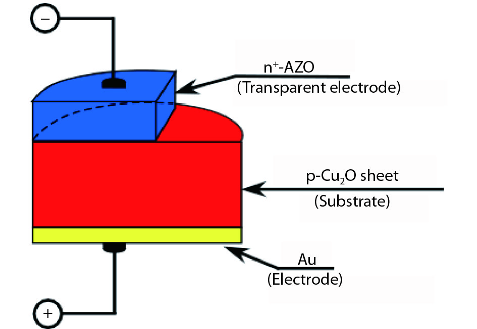
J. Semicond. > 2019, Volume 40 > Issue 3 > 032701

ARTICLES

Photovoltaic properties of Cu2O-based heterojunction solar cells using n-type oxide semiconductor nano thin films prepared by low damage magnetron sputtering method

Toshihiro Miyata, Kyosuke Watanabe, Hiroki Tokunaga and Tadatsugu Minami

+ Author Affiliations

 Corresponding author: Toshihiro Miyata, email: tmiyata@neptune.kanazawa-it.ac.jp

DOI: 10.1088/1674-4926/40/3/032701

PDF

Turn off MathJax

Abstract: We improved the photovoltaic properties of Cu2O-based heterojunction solar cells using n-type oxide semiconductor thin films prepared by a sputtering apparatus with our newly developed multi-chamber system. We also obtained the highest efficiency (3.21%) in an AZO/p-Cu2O heterojunction solar cell prepared with optimized pre-sputtering conditions using our newly developed multi-chamber sputtering system. This value achieves the same or higher characteristics than AZO/Cu2O solar cells with a similar structure prepared by the pulse laser deposition method.

Key words: Cu2OAZOsolar celloxide thin filmmagnetron sputtering

Since p-type cuprous oxide (p-Cu2O) has a high theoretical conversion efficiency of about 20%, it has long attracted research attention as a solar cell material[19]. In addition, solar cells based on p-Cu2O have attracted significant interest owing to the material’s nontoxicity, its suitability for sustainable semiconductor material usage, and its potential for cost-effective manufacturing[1017]. We previously achieved significantly enhanced efficiencies in n-type Al-doped ZnO (AZO)/p-Cu2O heterojunction solar cells fabricated by depositing an AZO thin film on a thermally oxidized p-Cu2O sheet using low-damage and -temperature deposition techniques[1820]. Using pulsed-laser deposition (PLD) at room temperature (RT), AZO thin films have been fabricated not only as n-type semiconductor window layers but also as transparent electrodes in heterojunction solar cells, which exhibited efficiencies exceeding 3%[21]. However, PLD methods suffer from technical disadvantages for the practical fabrication technology of solar cells, such as a low deposition rate and complicated large area deposition. On the other hand, the magnetron sputtering (MSD) method easily prepared the large area deposition and obtained a high deposition rate. But the photovoltaic properties of the Cu2O-based heterojunction solar cells fabricated by it were poorer than those of PLD.

In this paper, we describe the improvement of the photovoltaic properties of Cu2O-based heterojunction solar cells using AZO thin films prepared by the sputtering apparatus with our newly developed multi-chamber system.

Cu2O sheets were prepared by oxidizing copper sheets (0.2-mm thick with 99.96% purity) using heat treatment in a furnace with a controlled ambient atmosphere, described in detail elsewhere[1820].

To incorporate Na into the oxidized Cu2O sheets, the sheets impregnated with NaCl powder (purity: 99.9%, KANTO KAGAKU Co. Ltd.) were heat-treated at 700 °C in an Ar gas atmosphere for 1 h[22]. After cooling to 500 °C, the Cu2O sheets were exposed to air at RT. The resulting sodium-doped Cu2O (Cu2O:Na) sheets were polycrystalline p-type semiconductors with a hole concentration of the order of 1015 cm−3 and a Hall mobility as high as 100 cm2V−1s−1. Since the carrier concentration of the Cu2O sheet can be controlled by Na doping[15], we carried out Na doping to optimize the carrier concentration of the Cu2O sheet. We prepared transparent conducting AZO thin films on p-Cu2O sheets using a multi-chamber MSD apparatus. The AZO thin film is not only an n-type semiconductor layer but also a transparent electrode. The multi-chamber MSD apparatus, which has loading and deposition chambers, used a direct current (DC) and a radio frequency (RF, 13.56 MHz) power supply that was applied either separately or together. The deposition was performed at RT using a target-substrate distance of 10–40 mm; the targets were a sintered AZO (Al2O3 content 2 wt %, Tosoh Speciality Materials Corp.) in a pure Ar gas atmosphere at pressures of 0.2 and 0–8 Pa. The 200-nm-thick AZO thin films, which functioned not only as an n-type layer but also as transparent electrodes, exhibited resistivity of the order of 10−3 Ωcm and a carrier concentration of the order of 1020 cm−3. To evaluate the electrical and optical properties of the resulting AZO thin films, simultaneous and/or additional depositions were also conducted on glass substrates. Solar cells were fabricated by forming an AZO/p-Cu2O:Na structure on the front surface of the Cu2O:Na sheets and an Au ohmic electrode on the back surface (Fig. 1). The solar cell with the AZO/Cu2O structure (Fig. 1) had a type II heterojunction structure based on the measurement results of the work functions of AZO and Cu2O by X-Ray Photoelectron Sepctroscopy (XPS, ULVAC-PHI, model 1600). The photovoltaic properties of the Cu2O-based solar cells (electrode area of 3.14 mm2) were evaluated by exposing only the AZO transparent electrode area to AM1.5G solar illumination (100 mW/cm2, Asahi Spectra, model HAL320) at 25 °C.

Figure  1.  (Color online) Cross-sectional structure of AZO/p-Cu2O solar cell.

When an AZO layer is formed on a p-Cu2O sheet by the magnetron sputtering method, the following two causes are considered the cause of the deterioration of the photovoltaic properties: (1) the physical damage on the Cu2O sheet surface due to bombardment by the sputtered particles; (2) excessive oxidation of the Cu2O sheet surface by oxygen ions. Fig. 2 shows the typical current–voltage (J–V) characteristics of the AZO/p-Cu2O heterojunction solar cells prepared with different target-Cu2O sheet distances. It should be noted that the J–V characteristics of the AZO thin film/p-Cu2O heterojunction solar cells were dependent on the target-Cu2O sheet distance. Fig. 3 shows the conversion efficiency (η), the fill factor (FF), VOC, and JSC as functions of the target-Cu2O sheet distance for AZO/p-Cu2O heterojunction solar cells fabricated with a target-Cu2O sheet distance from 30 to 55 mm. The photovoltaic properties did not substantially change until the distance between the target Cu2O sheets became about 35 mm. However, as the distance further increased, the photovoltaic properties gradually decreased. By increasing the distance between the substrate targets, we expect to reduce the physical damage on the surface of the Cu2O sheet due to the bombardment. Unfortunately, the photovoltaic properties deteriorated. This result suggests that the deterioration of the photovoltaic property accompanying the increase in the distance between the target and the substrate is not primarily caused by the physical damage on the Cu2O sheet’s surface due to the bombardment. In addition, Fig. 4 shows the typical J–V characteristics for AZO/p-Cu2O heterojunction solar cells prepared with different sputtering voltages: 380 and 700 V. It should be noted that the J–V characteristics of the AZO thin film/p-Cu2O heterojunction solar cells were strongly dependent on the sputtering voltage. As the sputtering voltage increases, the bombardment effect is expected to increase, but the photovoltaic characteristics will slightly improve. Fig. 5 shows the J–V characteristics measured under dark conditions obtained in an AZO/p-Cu2O heterojunction solar cell (Fig. 4), and when reverse bias voltage was applied, the leakage current decreased in the AZO/p-Cu2O solar cell fabricated by forming AZO film with higher sputtering voltage. This suggests that an improvement of the p-n junction, as seen in the AZO/Cu2O heterojunction, was achieved by a higher sputtering voltage. These above results suggest that the cause of the deterioration of the photovoltaic property of the AZO/p-Cu2O solar cell, fabricated by forming AZO thin film on the Cu2O sheet by the sputtering method, is not the physical bombardment of the sputtering particles. The cause of the deterioration of the photoelectric conversion characteristics of the AZO/p-Cu2O solar cell, where AZO thin film is formed on the Cu2O sheet by the sputtering method, is mainly attributable to excessive oxidation of the Cu2O sheet’s surface by chemically active oxygen ions to the p-n junction interface.

Figure  2.  (Color online) Typical J–V characteristics for AZO/p-Cu2O heterojunction solar cells prepared with different target-Cu2O sheet distances.
Figure  3.  (Color online) Conversion efficiency (η), fill factor (FF), VOC, and JSC as functions of target-Cu2O sheet distance for AZO/p-Cu2O heterojunction solar cells.
Figure  4.  (Color online) Typical J–V characteristics for AZO/p-Cu2O heterojunction solar cells prepared with different sputtering voltages: 380 and 700 V.
Figure  5.  (Color online) J–V characteristics measured under dark conditions obtained in AZO/p-Cu2O heterojunction solar cell shown in Fig. 4.

As mentioned above, to improve the photovoltaic property of the AZO/p-Cu2O solar cell fabricated by forming AZO thin film by the sputtering method, the Cu2O sheet surface’s excessive oxidation must be reduced by oxygen ions. However, in the AZO thin film deposition process by the sputtering method, to remove oxygen and moisture from the target surface, we must process the generated plasma using pre-sputtering. In this pre-sputtering process, the Cu2O sheet’s surface is protected by a shutter, but since the sputtering gas pressure is as high as 0.6 Pa, preventing excessive oxidation of the Cu2O’s surface is difficult by a shutter due to plasma wraparound. Our newly developed multi-chamber sputtering apparatus has deposition and loading chambers, and we can prevent excessive oxidation by oxygen ions by retracting the Cu2O sheet into the loading chamber during the pre-sputtering process.

As one example, as a function of the pre-sputtering time, typical J–V characteristics are shown in Fig. 6 for AZO/p-Cu2O heterojunction solar cells measured under AM1.5G solar illumination. Pre-sputtering was carried out in a deposition chamber before introducing the p-Cu2O sheet from the loading chamber. Next a p-Cu2O sheet was introduced into the deposition chamber, and then the n+-AZO thin films were prepared at RT at a pure Ar pressure of 0.6 Pa. As seen in Fig. 6, we drastically improved the J–V characteristics by increasing the pre-sputtering time to 10 min. These results suggest that the p-Cu2O sheet’s surface was degraded by exposure to excessive oxygen plasma in the deposition chamber without the pre-sputtering process. On the other hand, when pre-sputtering was performed for more than 15 min, the amount of oxygen, supplied from the moisture adsorbed on the target surface, decreased. As a result, oxygen was deprived on the Cu2O surface, and the interface state deteriorated. We obtained the highest efficiency of 3.21% in an AZO/p-Cu2O heterojunction solar cell prepared with a 10 min pre-sputtering time. Fig. 6 also shows typical J–V characteristics for AZO/p-Cu2O heterojunction solar cells prepared using PLD. The J–V characteristics of the AZO/p-Cu2O heterojunction solar cells, prepared using the sputtering method with 10 min pre-sputtering, exhibited better properties than the PLD method (Fig. 6). The solar cell’s leakage current prepared by magnetron sputtering with 10 min pre-sputtering, measured under a reversed bias, was as low as the solar cell prepared by PLD. This suggests that greater improvement of the p–n junction, as seen in the AZO/Cu2O heterojunction, can be achieved by magnetron sputtering methods with 10 min pre-sputtering to decrease the recombination associated with defects at the interface between AZO and Cu2O.

Figure  6.  (Color online) Typical J–V characteristics as a function of pre-sputtering time for AZO/p-Cu2O heterojunction solar cells.

We demonstrated that using a newly developed multi-chamber sputtering apparatus for preparing AZO thin film not only as the n-type semiconductor layer but also as a transparent electrode greatly improves the performance of AZO/p-Cu2O heterojunction solar cells. We significantly improved the photovoltaic properties by AZO/p-Cu2O heterojunction solar cells fabricated on p-type Cu2O sheets that were prepared by the thermal oxidation of Cu sheets. The high efficiency obtained in the heterojunction solar cells may be attributable to a decrease of the defect levels at the interface between the AZO thin film and the Cu2O sheet. The highest efficiency (3.21%) was obtained in an AZO/p-Cu2O heterojunction solar cell. This value achieved the same or higher characteristics than the solar cell with a similar structure prepared by the PLD method. Therefore, the newly developed multi-chamber sputtering apparatus is promising as a practical n-type semiconductor thin film that forms technology for Cu2O-based solar cells.

The authors acknowledge the technical assistance of R. Takahashi and N. Ogawa in the experiments. This research was partly supported by Grant-in-Aid for Scientific Research on Innovative Areas from the Ministry of Education, Culture, Sports, Science and Technology of Japan (No.15K04723).


[1]
N Asima, K Sopiana, S Ahmadib, et al. A review on the role of materials science in solar cells. Renew Sustain Energy Rev, 2012, 16: 5834. doi: 10.1016/j.rser.2012.06.004
[2]
A E Rakhshani. Preparation, characteristics and photovoltaic properties of cuprous oxide – a review. Solid-State Electron, 1986, 29: 7. doi: 10.1016/0038-1101(86)90191-7
[3]
G P Pollack. D Trivichi. Photoelectric properties of cuprous oxide. J Appl Phys, 1975, 46: 163. doi: 10.1063/1.321312
[4]
J Herion, E A Niekisch, G Scharl. Investigation of metal oxide/cuprous oxide heterojunction solar cells. Sol Energy Mater, 1980, 4: 101. doi: 10.1016/0165-1633(80)90022-2
[5]
L Papadimitriou, N A Economou, D Trivich. Heterojunction solar cells on cuprous oxide. Sol Cells, 1981, 3: 73. doi: 10.1016/0379-6787(81)90084-3
[6]
L C Olsen, F W Addis, W Miller. Experimental and theoretical studies of Cu2O solar cells. Sol Cells, 1982, 7: 247. doi: 10.1016/0379-6787(82)90050-3
[7]
W M Sears, E Fortin, J B Webb. Indium tin oxide/Cu2O photovoltaic cells. Thin Solid Films, 1983,103: 303. doi: 10.1016/0040-6090(83)90447-9
[8]
B P Rai. Cu2O solar cells: A review. Sol Cells, 1988, 25: 265. doi: 10.1016/0379-6787(88)90065-8
[9]
R N Briskman. A study of electrodeposited cuprous oxide photovoltaic cells. Sol Energy Mater Sol Cells, 1992, 27: 361. doi: 10.1016/0927-0248(92)90097-9
[10]
T Minami, Y Nishi, T Miyata, et al. High-efficiency oxide solar cells with ZnO/Cu2O heterojunction fabricated on thermally oxidized Cu2O sheets. Appl Phys Express, 2011, 4: 062301. doi: 10.1143/APEX.4.062301
[11]
Y S Lee, J Heo, S C Siah, et al. Ultrathin amorphous zinc-tin-oxide buffer layer for enhancing heterojunction interface quality in metal-oxide solar cells. Energy Environ Sci, 2013, 6: 2112. doi: 10.1039/c3ee24461j
[12]
T Minami, Y Nishi, T Miyata. High-efficiency Cu2O-based heterojunction solar cells fabricated using a Ga2O3 thin film as n-type layer. Appl Phys Express, 2013, 6: 044101. doi: 10.7567/APEX.6.044101
[13]
S W Lee, Y S Lee, J Heo, et al. Improved Cu2O-based solar cells using atomic layer deposition to control the Cu oxidation state at the p-n junction. Adv Energy Mater, 2014, 4: 1301916. doi: 10.1002/aenm.201301916
[14]
Y S Lee, D Chua, R E Brandt, et al. Atomic layer deposited gallium oxide buffer layer enables 1.2 V open-circuit voltage in cuprous oxide solar cells. Adv Mater, 2014, 26: 4704. doi: 10.1002/adma.v26.27
[15]
T Minami, Y Nishi, T Miyata. Heterojunction solar cell with 6% efficiency based on an n-type aluminum–gallium–oxide thin film and p-type sodium-doped Cu2O sheet. Appl Phys Express, 2015, 8: 022301. doi: 10.7567/APEX.8.022301
[16]
Y Ievskaya, R L Z Hoye, A Sadhanala, et al. Fabrication of ZnO/Cu2O heterojunctions in atmospheric conditions: Improved interface quality and solar cell performanceSol. Energy Mater Sol Cells, 2015, 135: 43. doi: 10.1016/j.solmat.2014.09.018
[17]
R L Z Hoye, R E Brandt, Y Ievskaya, et al. Perspective: Maintaining surface-phase purity is key to efficient open air fabricated cuprous oxide solar cells. APL Mater, 2015, 3: 020901. doi: 10.1063/1.4913442
[18]
T Minami, T Miyata, Y Nishi. Efficiency improvement of Cu2O-based heterojunction solar cells fabricated using thermally oxidized copper sheets. Thin Solid Films, 2014, 559: 105. doi: 10.1016/j.tsf.2013.11.026
[19]
T Minami, T Miyata, Y Nishi. Cu2O-based heterojunction solar cells with an Al-doped ZnO/oxide semiconductor/thermally oxidized Cu2O sheet structure. Sol Energy, 2014, 105: 206. doi: 10.1016/j.solener.2014.03.036
[20]
T Minami, Y Nishi, T Miyata. Cu2O-based solar cells using oxide semiconductors. J Semicond, 2016, 37: 014002. doi: 10.1088/1674-4926/37/1/014002
[21]
Nishi Y, Miyata T, Nomoto J, et al. High-efficiency Cu2O-based heterojunction solar cells fabricated on thermally oxidized copper sheet. Conf Rec 37th IEEE Photovoltaic Specialists Conf, 2011, 266
[22]
T. Minami, Y. Nishi, and T. Miyata. Impact of incorporating sodium into polycrystalline p-type Cu2O for heterojunction solar cell applications. Appl Phys Lett, 2014, 105: 212104. doi: 10.1063/1.4902879
Fig. 1.  (Color online) Cross-sectional structure of AZO/p-Cu2O solar cell.

Fig. 2.  (Color online) Typical J–V characteristics for AZO/p-Cu2O heterojunction solar cells prepared with different target-Cu2O sheet distances.

Fig. 3.  (Color online) Conversion efficiency (η), fill factor (FF), VOC, and JSC as functions of target-Cu2O sheet distance for AZO/p-Cu2O heterojunction solar cells.

Fig. 4.  (Color online) Typical J–V characteristics for AZO/p-Cu2O heterojunction solar cells prepared with different sputtering voltages: 380 and 700 V.

Fig. 5.  (Color online) J–V characteristics measured under dark conditions obtained in AZO/p-Cu2O heterojunction solar cell shown in Fig. 4.

Fig. 6.  (Color online) Typical J–V characteristics as a function of pre-sputtering time for AZO/p-Cu2O heterojunction solar cells.

[1]
N Asima, K Sopiana, S Ahmadib, et al. A review on the role of materials science in solar cells. Renew Sustain Energy Rev, 2012, 16: 5834. doi: 10.1016/j.rser.2012.06.004
[2]
A E Rakhshani. Preparation, characteristics and photovoltaic properties of cuprous oxide – a review. Solid-State Electron, 1986, 29: 7. doi: 10.1016/0038-1101(86)90191-7
[3]
G P Pollack. D Trivichi. Photoelectric properties of cuprous oxide. J Appl Phys, 1975, 46: 163. doi: 10.1063/1.321312
[4]
J Herion, E A Niekisch, G Scharl. Investigation of metal oxide/cuprous oxide heterojunction solar cells. Sol Energy Mater, 1980, 4: 101. doi: 10.1016/0165-1633(80)90022-2
[5]
L Papadimitriou, N A Economou, D Trivich. Heterojunction solar cells on cuprous oxide. Sol Cells, 1981, 3: 73. doi: 10.1016/0379-6787(81)90084-3
[6]
L C Olsen, F W Addis, W Miller. Experimental and theoretical studies of Cu2O solar cells. Sol Cells, 1982, 7: 247. doi: 10.1016/0379-6787(82)90050-3
[7]
W M Sears, E Fortin, J B Webb. Indium tin oxide/Cu2O photovoltaic cells. Thin Solid Films, 1983,103: 303. doi: 10.1016/0040-6090(83)90447-9
[8]
B P Rai. Cu2O solar cells: A review. Sol Cells, 1988, 25: 265. doi: 10.1016/0379-6787(88)90065-8
[9]
R N Briskman. A study of electrodeposited cuprous oxide photovoltaic cells. Sol Energy Mater Sol Cells, 1992, 27: 361. doi: 10.1016/0927-0248(92)90097-9
[10]
T Minami, Y Nishi, T Miyata, et al. High-efficiency oxide solar cells with ZnO/Cu2O heterojunction fabricated on thermally oxidized Cu2O sheets. Appl Phys Express, 2011, 4: 062301. doi: 10.1143/APEX.4.062301
[11]
Y S Lee, J Heo, S C Siah, et al. Ultrathin amorphous zinc-tin-oxide buffer layer for enhancing heterojunction interface quality in metal-oxide solar cells. Energy Environ Sci, 2013, 6: 2112. doi: 10.1039/c3ee24461j
[12]
T Minami, Y Nishi, T Miyata. High-efficiency Cu2O-based heterojunction solar cells fabricated using a Ga2O3 thin film as n-type layer. Appl Phys Express, 2013, 6: 044101. doi: 10.7567/APEX.6.044101
[13]
S W Lee, Y S Lee, J Heo, et al. Improved Cu2O-based solar cells using atomic layer deposition to control the Cu oxidation state at the p-n junction. Adv Energy Mater, 2014, 4: 1301916. doi: 10.1002/aenm.201301916
[14]
Y S Lee, D Chua, R E Brandt, et al. Atomic layer deposited gallium oxide buffer layer enables 1.2 V open-circuit voltage in cuprous oxide solar cells. Adv Mater, 2014, 26: 4704. doi: 10.1002/adma.v26.27
[15]
T Minami, Y Nishi, T Miyata. Heterojunction solar cell with 6% efficiency based on an n-type aluminum–gallium–oxide thin film and p-type sodium-doped Cu2O sheet. Appl Phys Express, 2015, 8: 022301. doi: 10.7567/APEX.8.022301
[16]
Y Ievskaya, R L Z Hoye, A Sadhanala, et al. Fabrication of ZnO/Cu2O heterojunctions in atmospheric conditions: Improved interface quality and solar cell performanceSol. Energy Mater Sol Cells, 2015, 135: 43. doi: 10.1016/j.solmat.2014.09.018
[17]
R L Z Hoye, R E Brandt, Y Ievskaya, et al. Perspective: Maintaining surface-phase purity is key to efficient open air fabricated cuprous oxide solar cells. APL Mater, 2015, 3: 020901. doi: 10.1063/1.4913442
[18]
T Minami, T Miyata, Y Nishi. Efficiency improvement of Cu2O-based heterojunction solar cells fabricated using thermally oxidized copper sheets. Thin Solid Films, 2014, 559: 105. doi: 10.1016/j.tsf.2013.11.026
[19]
T Minami, T Miyata, Y Nishi. Cu2O-based heterojunction solar cells with an Al-doped ZnO/oxide semiconductor/thermally oxidized Cu2O sheet structure. Sol Energy, 2014, 105: 206. doi: 10.1016/j.solener.2014.03.036
[20]
T Minami, Y Nishi, T Miyata. Cu2O-based solar cells using oxide semiconductors. J Semicond, 2016, 37: 014002. doi: 10.1088/1674-4926/37/1/014002
[21]
Nishi Y, Miyata T, Nomoto J, et al. High-efficiency Cu2O-based heterojunction solar cells fabricated on thermally oxidized copper sheet. Conf Rec 37th IEEE Photovoltaic Specialists Conf, 2011, 266
[22]
T. Minami, Y. Nishi, and T. Miyata. Impact of incorporating sodium into polycrystalline p-type Cu2O for heterojunction solar cell applications. Appl Phys Lett, 2014, 105: 212104. doi: 10.1063/1.4902879
1

Magnetron sputtering NiOx for perovskite solar cells

Xiangyi Shen, Xinwu Ke, Yingdong Xia, Qingxun Guo, Yonghua Chen, et al.

Journal of Semiconductors, 2025, 46(5): 051803. doi: 10.1088/1674-4926/24100032

2

Substrate temperature dependent studies on properties of chemical spray pyrolysis deposited CdS thin films for solar cell applications

Kiran Diwate, Amit Pawbake, Sachin Rondiya, Rupali Kulkarni, Ravi Waykar, et al.

Journal of Semiconductors, 2017, 38(2): 023001. doi: 10.1088/1674-4926/38/2/023001

3

ZnO1-xTex and ZnO1-xSx semiconductor alloys as competent materials for opto-electronic and solar cell applications:a comparative analysis

Utsa Das, Partha P. Pal

Journal of Semiconductors, 2017, 38(8): 082001. doi: 10.1088/1674-4926/38/8/082001

4

ZnSe/ITO thin films:candidate for CdTe solar cell window layer

A.A. Khurram, M. Imran, Nawazish A. Khan, M. Nasir Mehmood

Journal of Semiconductors, 2017, 38(9): 093001. doi: 10.1088/1674-4926/38/9/093001

5

Cu2O-based solar cells using oxide semiconductors

Tadatsugu Minami, Yuki Nishi, Toshihiro Miyata

Journal of Semiconductors, 2016, 37(1): 014002. doi: 10.1088/1674-4926/37/1/014002

6

The calculation of band gap energy in zinc oxide films

Ali Arif, Okba Belahssen, Salim Gareh, Said Benramache

Journal of Semiconductors, 2015, 36(1): 013001. doi: 10.1088/1674-4926/36/1/013001

7

β-FeSi2 films prepared on 6H-SiC substrates by magnetron sputtering

Hong Li, Hongbin Pu, Chunlei Zheng, Zhiming Chen

Journal of Semiconductors, 2015, 36(6): 063005. doi: 10.1088/1674-4926/36/6/063005

8

Structural and optical properties of Zn3N2 films prepared by magnetron sputtering in NH3-Ar mixture gases

Wu Jiangyan, Yan Jinliang, Yue Wei, Li Ting

Journal of Semiconductors, 2012, 33(4): 043001. doi: 10.1088/1674-4926/33/4/043001

9

Preparation and characterization of transparent conducting ZnO:W films by DC magnetron sputtering

Zhang Huafu, Yang Shugang, Liu Hanfa, Yuan Changkun

Journal of Semiconductors, 2011, 32(4): 043002. doi: 10.1088/1674-4926/32/4/043002

10

Annealing effects on the formation of semiconducting Mg2Si film using magnetron sputtering deposition

Xiao Qingquan, Xie Quan, Chen Qian, Zhao Kejie, Yu Zhiqiang, et al.

Journal of Semiconductors, 2011, 32(8): 082002. doi: 10.1088/1674-4926/32/8/082002

11

Optical and electrical properties of porous silicon layer formed on the textured surface by electrochemical etching

Ou Weiying, Zhao Lei, Diao Hongwei, Zhang Jun, Wang Wenjing, et al.

Journal of Semiconductors, 2011, 32(5): 056002. doi: 10.1088/1674-4926/32/5/056002

12

An MWCNT-doped SnO2 thin film NO2 gas sensor by RF reactive magnetron sputtering

Lin Wei, Huang Shizhen, Chen Wenzhe

Journal of Semiconductors, 2010, 31(2): 024006. doi: 10.1088/1674-4926/31/2/024006

13

Thickness dependence of the properties of transparent conducting ZnO:Zr films deposited on flexible substrates by RF magnetron sputtering

Zhang Huafu, Lei Chengxin, Liu Hanfa, Yuan Changkun

Journal of Semiconductors, 2009, 30(4): 043004. doi: 10.1088/1674-4926/30/4/043004

14

Novel approach for characterizing the specific shunt resistance caused by the penetration of the front contact through the p–n junction in solar cell

Zhang Lucheng, Shen Hui

Journal of Semiconductors, 2009, 30(7): 074007. doi: 10.1088/1674-4926/30/7/074007

15

Boron-doped silicon film as a recombination layer in the tunnel junction of a tandem solar cell

Shi Mingji, Wang Zhanguo, Liu Shiyong, Peng Wenbo, Xiao Haibo, et al.

Journal of Semiconductors, 2009, 30(6): 063001. doi: 10.1088/1674-4926/30/6/063001

16

Influence of the sputtering pressure on the properties of transparent conducting zirconium-doped zinc oxide films prepared by RF magnetron sputtering

Liu Hanfa, Zhang Huafu, Lei Chengxin, Yuan Changkun

Journal of Semiconductors, 2009, 30(2): 023001. doi: 10.1088/1674-4926/30/2/023001

17

Influence of Sputtering Pressure on the Properties of ZnO:Ga Films Prepared by DC Reactive Magnetron Sputtering

Ma Quanbao, Zhu Liping, Ye Zhizhen, He Haiping, Wang Jingrui, et al.

Chinese Journal of Semiconductors , 2007, 28(S1): 285-288.

18

Influence of Ag Layer Thickness on the Properties of ZnO/Ag/ZnO Films

Li Jun, Yan Jinliang, Sun Xueqing, Li Kewei, Yang Chunxiu, et al.

Chinese Journal of Semiconductors , 2007, 28(9): 1402-1405.

19

Electrical and Optical Properties of Cu2 ZnSnS4 Thin Films Prepared for Solar Cell Absorber

Shao Lexi, Fu Yujun, Zhang Jun, He Deyan

Chinese Journal of Semiconductors , 2007, 28(S1): 337-340.

20

Structural Characteristic of CdS Thin films and Their Influence on Cu(in,Ga)Se2(CIGS) Thin Film Solar Cell

Xue Yuming, Sun Yun, He Qing, Liu Fangfang, Li Changjian,and Ji Mingliang, et al.

Chinese Journal of Semiconductors , 2005, 26(2): 225-229.

1. Dabhi, S.D., Gahlot, S., Mirza, S. et al. Study of Anticancer Properties of Graphene Oxide–Metal Oxide Composite. Macromolecular Symposia, 2024, 413(1): 2300086. doi:10.1002/masy.202300086
2. Houng, B., Chung, C.L., Yeh, P.C. et al. Effect of annealing temperature on the properties of Cu2O thin films by RF magnetron sputter using Cu/Cu2O as composite targets. Journal of Ceramic Processing Research, 2023, 24(5): 788-795. doi:10.36410/jcpr.2023.24.5.788
3. Sliti, N., Touihri, S., Nguyen, N.D. Numerical modeling and analysis of AZO/Cu2O transparent solar cell with a TiO2 buffer layer. Engineering Research Express, 2023, 5(2): 025013. doi:10.1088/2631-8695/accacf
4. Zhang, J., Hou, Z.-L., Zhang, X. et al. Si@Cu composite anode material prepared by magnetron sputtering for high-capacity lithium-ion batteries. International Journal of Hydrogen Energy, 2022, 47(7): 4766-4771. doi:10.1016/j.ijhydene.2021.11.080
5. Du, J., Li, J., Liu, K. et al. Preparation and Characterization of Cu2O Thin Films by Electrodeposition in Acidic Media. Integrated Ferroelectrics, 2022, 229(1): 295-304. doi:10.1080/10584587.2022.2074238
6. Zakutayev, A., Major, J.D., Hao, X. et al. Emerging inorganic solar cell efficiency tables (version 2). JPhys Energy, 2021, 3(3): 032003. doi:10.1088/2515-7655/abebca
7. Nasori, N., Cao, D., Wang, Z. et al. Tunning of templated cuwo4 nanorods arrays thickness to improve photoanode water splitting. Molecules, 2021, 26(10): 2900. doi:10.3390/molecules26102900
8. Pang, X., Bai, H., Zhao, Y. et al. Photoelectrochemical detection of 4-nitrophenol by sensitive Ni/Cu2O photocathode. Electrochimica Acta, 2021. doi:10.1016/j.electacta.2020.137453
9. Zhang, J., Xue, W., Chen, X.-Y. et al. Sm doped BiFeO3 nanofibers for improved photovoltaic devices. Chinese Journal of Physics, 2020. doi:10.1016/j.cjph.2020.03.021
10. Kumar, R., Bergum, K., Riise, H.N. et al. Impact of post annealing and hydrogen implantation on functional properties of Cu2O thin films for photovoltaic applications. Journal of Alloys and Compounds, 2020. doi:10.1016/j.jallcom.2020.153982
11. Tiwari, P., Jaiswal, J., Chandra, R. Optical and electrical properties of highly ordered α-, γ- And α + γ-MnS films deposited by reactive sputtering technique. Journal of Applied Physics, 2019, 126(21): 213108. doi:10.1063/1.5127004
  • Search

    Advanced Search >>

    GET CITATION

    Toshihiro Miyata, Kyosuke Watanabe, Hiroki Tokunaga, Tadatsugu Minami. Photovoltaic properties of Cu2O-based heterojunction solar cells using n-type oxide semiconductor nano thin films prepared by low damage magnetron sputtering method[J]. Journal of Semiconductors, 2019, 40(3): 032701. doi: 10.1088/1674-4926/40/3/032701
    T Miyata, K Watanabe, H Tokunaga, T Minami, Photovoltaic properties of Cu2O-based heterojunction solar cells using n-type oxide semiconductor nano thin films prepared by low damage magnetron sputtering method[J]. J. Semicond., 2019, 40(3): 032701. doi: 10.1088/1674-4926/40/3/032701.
    shu

    Export: BibTex EndNote

    Article Metrics

    Article views: 4962 Times PDF downloads: 103 Times Cited by: 11 Times

    History

    Received: 15 June 2018 Revised: 29 September 2018 Online: Accepted Manuscript: 11 January 2019Uncorrected proof: 11 January 2019Published: 01 March 2019

    Catalog

      Email This Article

      User name:
      Email:*请输入正确邮箱
      Code:*验证码错误
      Toshihiro Miyata, Kyosuke Watanabe, Hiroki Tokunaga, Tadatsugu Minami. Photovoltaic properties of Cu2O-based heterojunction solar cells using n-type oxide semiconductor nano thin films prepared by low damage magnetron sputtering method[J]. Journal of Semiconductors, 2019, 40(3): 032701. doi: 10.1088/1674-4926/40/3/032701 ****T Miyata, K Watanabe, H Tokunaga, T Minami, Photovoltaic properties of Cu2O-based heterojunction solar cells using n-type oxide semiconductor nano thin films prepared by low damage magnetron sputtering method[J]. J. Semicond., 2019, 40(3): 032701. doi: 10.1088/1674-4926/40/3/032701.
      Citation:
      Toshihiro Miyata, Kyosuke Watanabe, Hiroki Tokunaga, Tadatsugu Minami. Photovoltaic properties of Cu2O-based heterojunction solar cells using n-type oxide semiconductor nano thin films prepared by low damage magnetron sputtering method[J]. Journal of Semiconductors, 2019, 40(3): 032701. doi: 10.1088/1674-4926/40/3/032701 ****
      T Miyata, K Watanabe, H Tokunaga, T Minami, Photovoltaic properties of Cu2O-based heterojunction solar cells using n-type oxide semiconductor nano thin films prepared by low damage magnetron sputtering method[J]. J. Semicond., 2019, 40(3): 032701. doi: 10.1088/1674-4926/40/3/032701.

      Photovoltaic properties of Cu2O-based heterojunction solar cells using n-type oxide semiconductor nano thin films prepared by low damage magnetron sputtering method

      DOI: 10.1088/1674-4926/40/3/032701
      More Information

      Catalog

        /

        DownLoad:  Full-Size Img  PowerPoint
        Return
        Return