


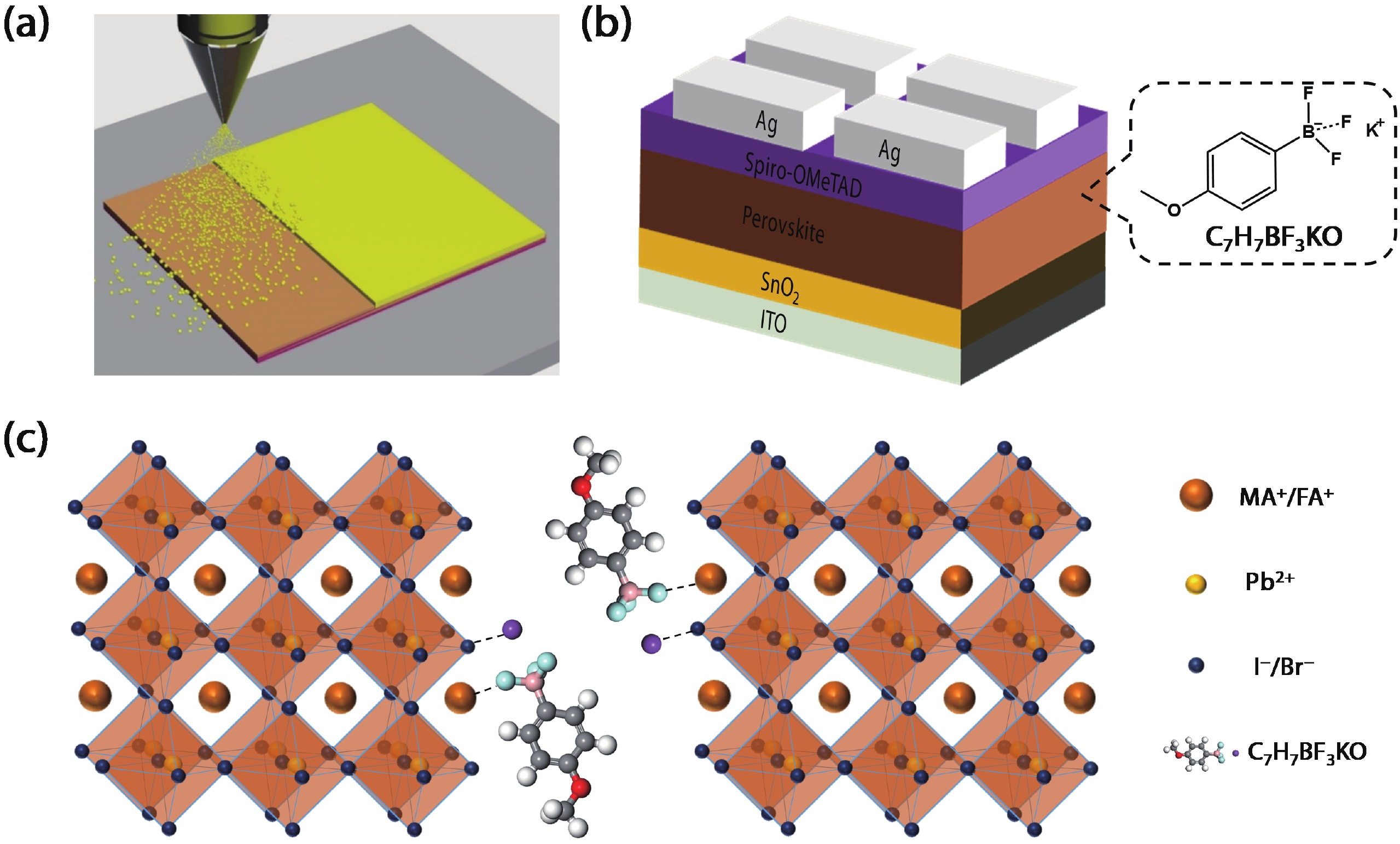
Fig. 1.
(Color online) (a) Schematic diagram of one-step spray-coating perovskite films. (b) Structure of the spray-coated devices. (c) Schematic diagram of the action of C7H7BF3KO.
ARTICLES
Chen Gao, Hui Wang, Pang Wang, Jinlong Cai, Yuandong Sun, Cong Yu, Teng Li, Xiaoshuai Zhang, Dan Liu and Tao Wang
Corresponding author: Tao Wang, twang@whut.edu.cn
Abstract: Defects as non-radiative recombination centers hinder the further efficiency improvements of perovskite solar cells (PSCs). Additive engineering has been demonstrated to be an effective method for defect passivation in perovskite films. Here, we employed (4-methoxyphenyl) potassium trifluoroborate (C7H7BF3KO) with ${{\rm{BF}}_3^-}$ and K+ functional groups to passivate spray-coated (FAPbI3)x(MAPbBr3)1–x perovskite and eliminate hysteresis. It is shown that the F of ${{\rm{BF}}_3^-}$ can form hydrogen bonds with the H atom in the amino group of MA+/FA+ ions of perovskite, thus reducing the generation of MA+/FA+ vacancies and improving device efficiency. Meanwhile, K+ and reduced MA+/FA+ vacancies can inhibit ion migration, thereby eliminating hysteresis. With the aid of C7H7BF3KO, we obtained hysteresis-free PSCs with the maximum efficiency of 19.5% by spray-coating in air. Our work demonstrates that additive engineering is promising to improve the performance of spray-coated PSCs.
Keywords: perovskite solar cells, spray-coating, additive engineering, defect passivation, hysteresis
| [1] |
Kojima A, Teshima K, Shirai Y, et al. Organometal halide perovskites as visible-light sensitizers for photovoltaic cells. J Am Chem Soc, 2009, 131, 6050 doi: 10.1021/ja809598r
|
| [2] |
NREL, Best Research-Cell Efficiency Chart. https://www.nrel.gov/pv/cell-efficiency.html (last access, January 26, 2022)
|
| [3] |
Zhao D W, Dai S J, Li M, et al. Improved efficiency and stability of perovskite solar cells using a difluorobenzothiadiazole-based interfacial material. ACS Appl Energy Mater, 2021, 4, 10646 doi: 10.1021/acsaem.1c01668
|
| [4] |
Zhang H K, Chen Z L, Qin M C, et al. Multifunctional crosslinking-enabled strain-regulating crystallization for stable, efficient α-FAPbI3-based perovskite solar cells. Adv Mater, 2021, 33, e2008487 doi: 10.1002/adma.202008487
|
| [5] |
Mo Y P, Wang C, Zheng X T, et al. Nitrogen-doped tin oxide electron transport layer for stable perovskite solar cells with efficiency over 23%. Interdiscip Mater, 2022, 1, 309 doi: 10.1002/idm2.12022
|
| [6] |
Zhang L X, Pan X Y, Liu L, et al. Star perovskite materials. J Semicond, 2022, 43, 030203 doi: 10.1088/1674-4926/43/3/030203
|
| [7] |
Cheng Y H, Xu X W, Xie Y M, et al. 18% high-efficiency air-processed perovskite solar cells made in a humid atmosphere of 70% RH. Sol RRL, 2017, 1, 1770131 doi: 10.1002/solr.201770131
|
| [8] |
Cheng Y H, So F, Tsang S W. Progress in air-processed perovskite solar cells: From crystallization to photovoltaic performance. Mater Horiz, 2019, 6, 1611 doi: 10.1039/C9MH00325H
|
| [9] |
Su J, Cai H K, Yang J T, et al. Perovskite ink with an ultrawide processing window for efficient and scalable perovskite solar cells in ambient air. ACS Appl Mater Interfaces, 2020, 12, 3531 doi: 10.1021/acsami.9b17141
|
| [10] |
Uličná S, Dou B J, Kim D H, et al. Scalable deposition of high-efficiency perovskite solar cells by spray-coating. ACS Appl Energy Mater, 2018, 1, 1853 doi: 10.1021/acsaem.8b00328
|
| [11] |
Zuo C T, Vak D, Angmo D C, et al. One-step roll-to-roll air processed high efficiency perovskite solar cells. Nano Energy, 2018, 46, 185 doi: 10.1016/j.nanoen.2018.01.037
|
| [12] |
Guo A Z, Chou L H, Yang S, et al. Ultrasonic spray-coatings: Multi-channel pumped ultrasonic spray-coating for high-throughput and scalable mixed halide perovskite solar cells. Adv Mater Interfaces, 2021, 8, 2170023 doi: 10.1002/admi.202170023
|
| [13] |
Bishop J E, Smith J A, Lidzey D G. Development of spray-coated perovskite solar cells. ACS Appl Mater Interfaces, 2020, 12, 48237 doi: 10.1021/acsami.0c14540
|
| [14] |
Su J, Cai H K, Ye X F, et al. Efficient perovskite solar cells prepared by hot air blowing to ultrasonic spraying in ambient air. ACS Appl Mater Interfaces, 2019, 11, 10689 doi: 10.1021/acsami.9b01843
|
| [15] |
Hilt F, Hovish M Q, Rolston N, et al. Rapid route to efficient, scalable, and robust perovskite photovoltaics in air. Energy Environ Sci, 2018, 11, 2102 doi: 10.1039/C8EE01065J
|
| [16] |
Bishop J E, Smith J A, Greenland C, et al. High-efficiency spray-coated perovskite solar cells utilizing vacuum-assisted solution processing. ACS Appl Mater Interfaces, 2018, 10, 39428 doi: 10.1021/acsami.8b14859
|
| [17] |
Cai H K, Liang X J, Ye X F, et al. High efficiency over 20% of perovskite solar cells by spray coating via a simple process. ACS Appl Energy Mater, 2020, 3, 9696 doi: 10.1021/acsaem.0c01129
|
| [18] |
Cassella E J, Spooner E L K, Thornber T, et al. Gas-assisted spray coating of perovskite solar cells incorporating sprayed self-assembled monolayers. Adv Sci, 2022, 9, e2104848 doi: 10.1002/advs.202104848
|
| [19] |
Zhang F, Zhu K. Additive engineering for efficient and stable perovskite solar cells. Adv Energy Mater, 2020, 10, 1902579 doi: 10.1002/aenm.201902579
|
| [20] |
Fu L, Li H, Wang L, et al. Defect passivation strategies in perovskites for an enhanced photovoltaic performance. Energy Environ Sci, 2020, 13, 4017 doi: 10.1039/D0EE01767A
|
| [21] |
Gao F, Zhao Y, Zhang X W, et al. Recent progresses on defect passivation toward efficient perovskite solar cells. Adv Energy Mater, 2020, 10, 1902650 doi: 10.1002/aenm.201902650
|
| [22] |
Chen B, Rudd P N, Yang S, et al. Imperfections and their passivation in halide perovskite solar cells. Chem Soc Rev, 2019, 48, 3842 doi: 10.1039/C8CS00853A
|
| [23] |
Byranvand M M, Saliba M. Defect passivation of perovskite films for highly efficient and stable solar cells. Sol RRL, 2021, 5, 2100295 doi: 10.1002/solr.202100295
|
| [24] |
Wu F, Pathak R, Qiao Q Q. Origin and alleviation of J-V hysteresis in perovskite solar cells: A short review. Catal Today, 2021, 374, 86 doi: 10.1016/j.cattod.2020.12.025
|
| [25] |
Liu P Y, Wang W, Liu S M, et al. Fundamental understanding of photocurrent hysteresis in perovskite solar cells. Adv Energy Mater, 2019, 9, 1803017 doi: 10.1002/aenm.201803017
|
| [26] |
Ren X X, Zhang L X, Yuan Y B, et al. Ion migration in perovskite solar cells. J Semicond, 2021, 42, 010201 doi: 10.1088/1674-4926/42/1/010201
|
| [27] |
Xiong S B, Hou Z Y, Zou S J, et al. Direct observation on p- to n-type transformation of perovskite surface region during defect passivation driving high photovoltaic efficiency. Joule, 2021, 5, 467 doi: 10.1016/j.joule.2020.12.009
|
| [28] |
Zhao Y C, Wei J, Li H, et al. A polymer scaffold for self-healing perovskite solar cells. Nat Commun, 2016, 7, 10228 doi: 10.1038/ncomms10228
|
| [29] |
Li X D, Ke S Z, Feng X X, et al. Enhancing the stability of perovskite solar cells through cross-linkable and hydrogen bonding multifunctional additives. J Mater Chem A, 2021, 9, 12684 doi: 10.1039/D1TA01572A
|
| [30] |
Li N X, Tao S X, Chen Y H, et al. Cation and anion immobilization through chemical bonding enhancement with fluorides for stable halide perovskite solar cells. Nat Energy, 2019, 4, 408 doi: 10.1038/s41560-019-0382-6
|
| [31] |
Abdi-Jalebi M, Andaji-Garmaroudi Z, Pearson A J, et al. Potassium- and rubidium-passivated alloyed perovskite films: Optoelectronic properties and moisture stability. ACS Energy Lett, 2018, 3, 2671 doi: 10.1021/acsenergylett.8b01504
|
| [32] |
Abdi-Jalebi M, Andaji-Garmaroudi Z, Cacovich S, et al. Maximizing and stabilizing luminescence from halide perovskites with potassium passivation. Nature, 2018, 555, 497 doi: 10.1038/nature25989
|
| [33] |
Zheng F, Chen W J, Bu T L, et al. Triggering the passivation effect of potassium doping in mixed-cation mixed-halide perovskite by light illumination. Adv Energy Mater, 2019, 9, 1901016 doi: 10.1002/aenm.201901016
|
| [34] |
Zhang M, Bing J M, Cho Y, et al. Synergistic effect of potassium and iodine from potassium triiodide complex additive on gas-quenched perovskite solar cells. Nano Energy, 2019, 63, 103853 doi: 10.1016/j.nanoen.2019.06.049
|
| [35] |
Bu T L, Li J, Li H Y, et al. Lead halide-templated crystallization of methylamine-free perovskite for efficient photovoltaic modules. Science, 2021, 372, 1327 doi: 10.1126/science.abh1035
|
| [36] |
Deng Y H, Zheng X P, Bai Y, et al. Surfactant-controlled ink drying enables high-speed deposition of perovskite films for efficient photovoltaic modules. Nat Energy, 2018, 3, 560 doi: 10.1038/s41560-018-0153-9
|
| [37] |
Gao C, Wang P, Wang H, et al. Binary additive engineering enables efficient perovskite solar cells via spray-coating in air. ACS Appl Energy Mater, 2021, 4, 11496 doi: 10.1021/acsaem.1c02235
|
| [38] |
Koo D, Cho Y, Kim U, et al. High-performance inverted perovskite solar cells with operational stability via n-type small molecule additive-assisted defect passivation. Adv Energy Mater, 2020, 10, 2001920 doi: 10.1002/aenm.202001920
|
| [39] |
Zhao M, Yan J, Yu G, et al. Grain boundary defects passivated with tert-butyl methacrylate for high-efficiency perovskite solar cells. ACS Appl Energy Mater, 2021, 4, 11298 doi: 10.1021/acsaem.1c02125
|
| [40] |
Wang H H, Wang Z W, Yang Z, et al. Ligand-modulated excess PbI2 nanosheets for highly efficient and stable perovskite solar cells. Adv Mater, 2020, 32, 2000865 doi: 10.1002/adma.202000865
|
| [41] |
Wang A L, Wang J W, Niu X B, et al. Inhibiting octahedral tilting for stable CsPbI2Br solar cells. InfoMat, 2022, 4, e12263 doi: 10.1002/inf2.12263
|
| [42] |
Hou M N, Xu Y Z, Zhou B, et al. Aryl diammonium iodide passivation for efficient and stable hybrid organ-inorganic perovskite solar cells. Adv Funct Mater, 2020, 30, 2002366 doi: 10.1002/adfm.202002366
|
| [43] |
Wu X Y, Jiang Y, Chen C, et al. Stable triple cation perovskite precursor for highly efficient perovskite solar cells enabled by interaction with 18C6 stabilizer. Adv Funct Mater, 2020, 30, 1908613 doi: 10.1002/adfm.201908613
|
| [44] |
Gao X X, Luo W, Zhang Y, et al. Stable and high-efficiency methylammonium-free perovskite solar cells. Adv Mater, 2020, 32, e1905502 doi: 10.1002/adma.201905502
|
| [45] |
Rao Y, Li Z P, Liu D C, et al. Dual-functional additive to simultaneously modify the interface and grain boundary for highly efficient and hysteresis-free perovskite solar cells. ACS Appl Mater Interfaces, 2021, 13, 20043 doi: 10.1021/acsami.1c01852
|
| [46] |
Chen Y L, Zuo X J, He Y Y, et al. Dual passivation of perovskite and SnO2 for high-efficiency MAPbI3 perovskite solar cells. Adv Sci, 2021, 8, 2001466 doi: 10.1002/advs.202001466
|
| [47] |
Sha Y M, Bi E B, Zhang Y, et al. A scalable integrated dopant-free heterostructure to stabilize perovskite solar cell modules. Adv Energy Mater, 2021, 11, 2003301 doi: 10.1002/aenm.202003301
|
| [48] |
Wang Y, Chen G Y, Ouyang D, et al. High phase stability in CsPbI3 enabled by Pb-I octahedra anchors for efficient inorganic perovskite photovoltaics. Adv Mater, 2020, 32, 2000186 doi: 10.1002/adma.202000186
|
| [49] |
Li X, Sheng W, Duan X, et al. Defect passivation effect of chemical groups on perovskite solar cells. ACS Appl Mater Interfaces, 2021, in press doi: 10.1021/acsami.1c08539
|
| [50] |
Liu X X, Cheng Y H, Tang B S, et al. Shallow defects levels and extract detrapped charges to stabilize highly efficient and hysteresis-free perovskite photovoltaic devices. Nano Energy, 2020, 71, 104556 doi: 10.1016/j.nanoen.2020.104556
|
| [51] |
Yuan J F, Bi C H, Wang S X, et al. Spray coating technologies: Spray-coated colloidal perovskite quantum dot films for highly efficient solar cells. Adv Funct Mater, 2019, 29, 1970337 doi: 10.1002/adfm.201970337
|
| [52] |
Dong Q F, Fang Y J, Shao Y C, et al. Solar cells. Electron-hole diffusion lengths > 175 μm in solution-grown CH3NH3PbI3 single crystals. Science, 2015, 347, 967 doi: 10.1126/science.aaa5760
|
| [53] |
Ye F H, Ma J J, Chen C, et al. Roles of MACl in sequentially deposited bromine-free perovskite absorbers for efficient solar cells. Adv Mater, 2021, 33, e2007126 doi: 10.1002/adma.202007126
|
| [54] |
Wang S J, Yang B W, Han J, et al. Polymeric room-temperature molten salt as a multifunctional additive toward highly efficient and stable inverted planar perovskite solar cells. Energy Environ Sci, 2020, 13, 5068 doi: 10.1039/D0EE02043E
|
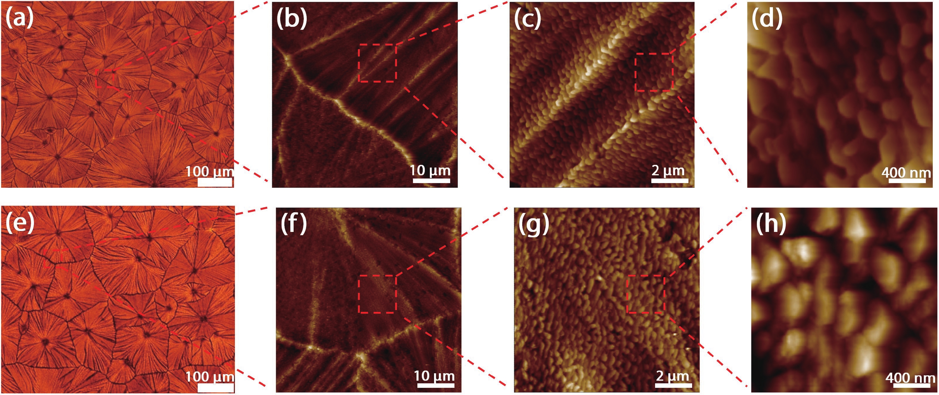
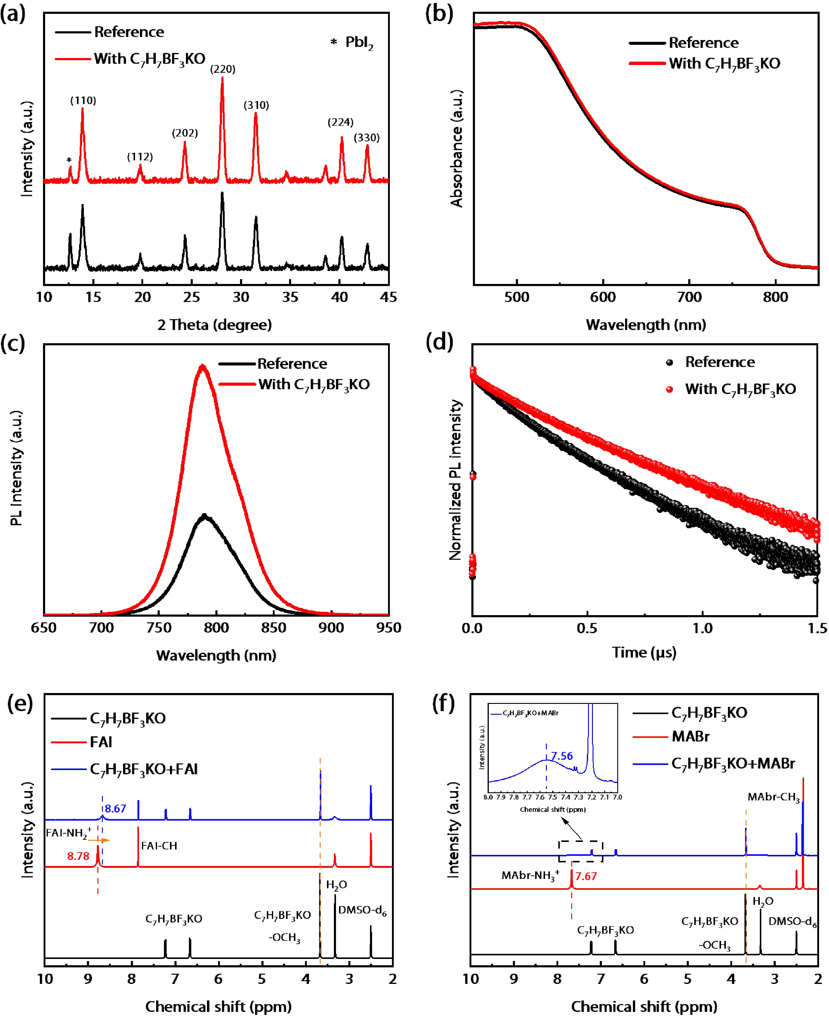
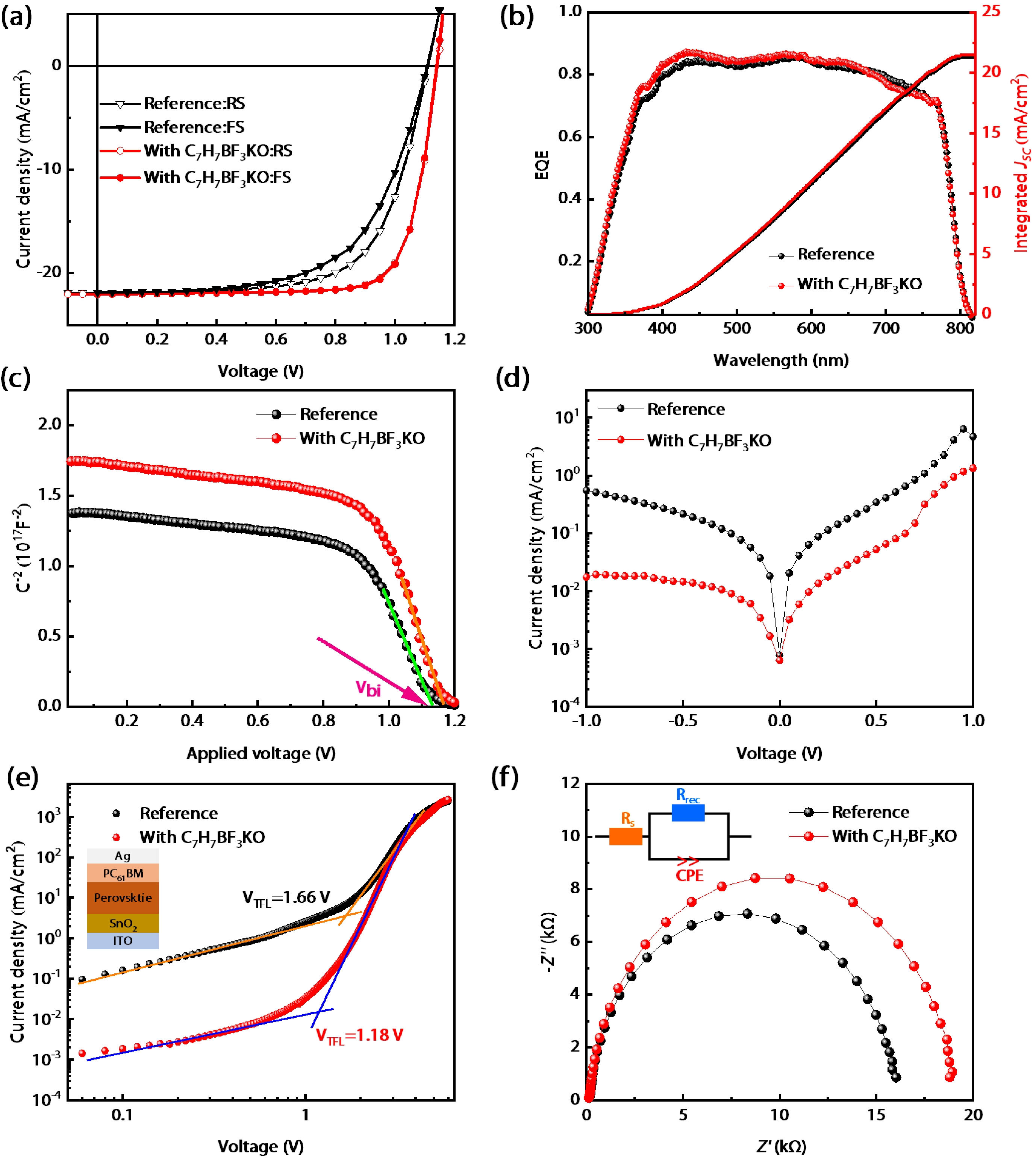
Table 1. The fitting parameters of TRPL for reference and C7H7BF3KO based spray-coated perovskite films.
| Additive | τ1 (ns) | A1 (%) | τ2 (ns) | A2 (%) | τave (ns) |
| w/o | 100 | 39 | 266 | 61 | 201 |
| C7H7BF3KO | 140 | 33 | 370 | 67 | 294 |
 DownLoad: CSV
Table 2. Summary of photovoltaic performance parameters of the reference and C7H7BF3KO based spray-coated PSCs.
| Additive | Scan direction | PCEmax (PCEave) (%) | FF (FFave) (%) | JSC (JSCave) (mA/cm2 ) | VOC (VOCave) (V) |
| w/o | reverse | 16.3 (14.7 ± 1.1) | 67.1 (62.0 ± 3.9) | 21.9 (21.6 ± 0.5) | 1.11 (1.09 ± 0.02) |
| forward | 14.9 (12.6 ± 1.2) | 61.6 (53.8 ± 4.5) | 21.9 (21.8 ± 0.5) | 1.11 (1.07 ± 0.02) | |
| C7H7BF3KO | reverse | 19.4 (17.6 ± 0.8) | 77.4 (72.4 ± 2.5) | 22.0 (21.8 ± 0.3) | 1.14 (1.11 ± 0.01) |
| forward | 19.5 (17.6 ± 0.9) | 77.8 (72.6 ± 3.1) | 22.0 (21.9 ± 0.3) | 1.14 (1.11 ± 0.01) |
DownLoad: CSV
Table 3. The fitting parameters of EIS for reference and C7H7BF3KO-based spray-coated perovskite devices.
| Additive | Rs (Ω·cm2) | Rrec (Ω·cm2) | CPE-T (F/cm2) | CPE-P |
| w/o | 156 | 15 886 | 9.80 × 10⁻⁹ | 0.93 |
| C7H7BF3KO | 136 | 18 972 | 7.62 × 10⁻⁹ | 0.93 |
DownLoad: CSV
| [1] |
Kojima A, Teshima K, Shirai Y, et al. Organometal halide perovskites as visible-light sensitizers for photovoltaic cells. J Am Chem Soc, 2009, 131, 6050 doi: 10.1021/ja809598r
|
| [2] |
NREL, Best Research-Cell Efficiency Chart. https://www.nrel.gov/pv/cell-efficiency.html (last access, January 26, 2022)
|
| [3] |
Zhao D W, Dai S J, Li M, et al. Improved efficiency and stability of perovskite solar cells using a difluorobenzothiadiazole-based interfacial material. ACS Appl Energy Mater, 2021, 4, 10646 doi: 10.1021/acsaem.1c01668
|
| [4] |
Zhang H K, Chen Z L, Qin M C, et al. Multifunctional crosslinking-enabled strain-regulating crystallization for stable, efficient α-FAPbI3-based perovskite solar cells. Adv Mater, 2021, 33, e2008487 doi: 10.1002/adma.202008487
|
| [5] |
Mo Y P, Wang C, Zheng X T, et al. Nitrogen-doped tin oxide electron transport layer for stable perovskite solar cells with efficiency over 23%. Interdiscip Mater, 2022, 1, 309 doi: 10.1002/idm2.12022
|
| [6] |
Zhang L X, Pan X Y, Liu L, et al. Star perovskite materials. J Semicond, 2022, 43, 030203 doi: 10.1088/1674-4926/43/3/030203
|
| [7] |
Cheng Y H, Xu X W, Xie Y M, et al. 18% high-efficiency air-processed perovskite solar cells made in a humid atmosphere of 70% RH. Sol RRL, 2017, 1, 1770131 doi: 10.1002/solr.201770131
|
| [8] |
Cheng Y H, So F, Tsang S W. Progress in air-processed perovskite solar cells: From crystallization to photovoltaic performance. Mater Horiz, 2019, 6, 1611 doi: 10.1039/C9MH00325H
|
| [9] |
Su J, Cai H K, Yang J T, et al. Perovskite ink with an ultrawide processing window for efficient and scalable perovskite solar cells in ambient air. ACS Appl Mater Interfaces, 2020, 12, 3531 doi: 10.1021/acsami.9b17141
|
| [10] |
Uličná S, Dou B J, Kim D H, et al. Scalable deposition of high-efficiency perovskite solar cells by spray-coating. ACS Appl Energy Mater, 2018, 1, 1853 doi: 10.1021/acsaem.8b00328
|
| [11] |
Zuo C T, Vak D, Angmo D C, et al. One-step roll-to-roll air processed high efficiency perovskite solar cells. Nano Energy, 2018, 46, 185 doi: 10.1016/j.nanoen.2018.01.037
|
| [12] |
Guo A Z, Chou L H, Yang S, et al. Ultrasonic spray-coatings: Multi-channel pumped ultrasonic spray-coating for high-throughput and scalable mixed halide perovskite solar cells. Adv Mater Interfaces, 2021, 8, 2170023 doi: 10.1002/admi.202170023
|
| [13] |
Bishop J E, Smith J A, Lidzey D G. Development of spray-coated perovskite solar cells. ACS Appl Mater Interfaces, 2020, 12, 48237 doi: 10.1021/acsami.0c14540
|
| [14] |
Su J, Cai H K, Ye X F, et al. Efficient perovskite solar cells prepared by hot air blowing to ultrasonic spraying in ambient air. ACS Appl Mater Interfaces, 2019, 11, 10689 doi: 10.1021/acsami.9b01843
|
| [15] |
Hilt F, Hovish M Q, Rolston N, et al. Rapid route to efficient, scalable, and robust perovskite photovoltaics in air. Energy Environ Sci, 2018, 11, 2102 doi: 10.1039/C8EE01065J
|
| [16] |
Bishop J E, Smith J A, Greenland C, et al. High-efficiency spray-coated perovskite solar cells utilizing vacuum-assisted solution processing. ACS Appl Mater Interfaces, 2018, 10, 39428 doi: 10.1021/acsami.8b14859
|
| [17] |
Cai H K, Liang X J, Ye X F, et al. High efficiency over 20% of perovskite solar cells by spray coating via a simple process. ACS Appl Energy Mater, 2020, 3, 9696 doi: 10.1021/acsaem.0c01129
|
| [18] |
Cassella E J, Spooner E L K, Thornber T, et al. Gas-assisted spray coating of perovskite solar cells incorporating sprayed self-assembled monolayers. Adv Sci, 2022, 9, e2104848 doi: 10.1002/advs.202104848
|
| [19] |
Zhang F, Zhu K. Additive engineering for efficient and stable perovskite solar cells. Adv Energy Mater, 2020, 10, 1902579 doi: 10.1002/aenm.201902579
|
| [20] |
Fu L, Li H, Wang L, et al. Defect passivation strategies in perovskites for an enhanced photovoltaic performance. Energy Environ Sci, 2020, 13, 4017 doi: 10.1039/D0EE01767A
|
| [21] |
Gao F, Zhao Y, Zhang X W, et al. Recent progresses on defect passivation toward efficient perovskite solar cells. Adv Energy Mater, 2020, 10, 1902650 doi: 10.1002/aenm.201902650
|
| [22] |
Chen B, Rudd P N, Yang S, et al. Imperfections and their passivation in halide perovskite solar cells. Chem Soc Rev, 2019, 48, 3842 doi: 10.1039/C8CS00853A
|
| [23] |
Byranvand M M, Saliba M. Defect passivation of perovskite films for highly efficient and stable solar cells. Sol RRL, 2021, 5, 2100295 doi: 10.1002/solr.202100295
|
| [24] |
Wu F, Pathak R, Qiao Q Q. Origin and alleviation of J-V hysteresis in perovskite solar cells: A short review. Catal Today, 2021, 374, 86 doi: 10.1016/j.cattod.2020.12.025
|
| [25] |
Liu P Y, Wang W, Liu S M, et al. Fundamental understanding of photocurrent hysteresis in perovskite solar cells. Adv Energy Mater, 2019, 9, 1803017 doi: 10.1002/aenm.201803017
|
| [26] |
Ren X X, Zhang L X, Yuan Y B, et al. Ion migration in perovskite solar cells. J Semicond, 2021, 42, 010201 doi: 10.1088/1674-4926/42/1/010201
|
| [27] |
Xiong S B, Hou Z Y, Zou S J, et al. Direct observation on p- to n-type transformation of perovskite surface region during defect passivation driving high photovoltaic efficiency. Joule, 2021, 5, 467 doi: 10.1016/j.joule.2020.12.009
|
| [28] |
Zhao Y C, Wei J, Li H, et al. A polymer scaffold for self-healing perovskite solar cells. Nat Commun, 2016, 7, 10228 doi: 10.1038/ncomms10228
|
| [29] |
Li X D, Ke S Z, Feng X X, et al. Enhancing the stability of perovskite solar cells through cross-linkable and hydrogen bonding multifunctional additives. J Mater Chem A, 2021, 9, 12684 doi: 10.1039/D1TA01572A
|
| [30] |
Li N X, Tao S X, Chen Y H, et al. Cation and anion immobilization through chemical bonding enhancement with fluorides for stable halide perovskite solar cells. Nat Energy, 2019, 4, 408 doi: 10.1038/s41560-019-0382-6
|
| [31] |
Abdi-Jalebi M, Andaji-Garmaroudi Z, Pearson A J, et al. Potassium- and rubidium-passivated alloyed perovskite films: Optoelectronic properties and moisture stability. ACS Energy Lett, 2018, 3, 2671 doi: 10.1021/acsenergylett.8b01504
|
| [32] |
Abdi-Jalebi M, Andaji-Garmaroudi Z, Cacovich S, et al. Maximizing and stabilizing luminescence from halide perovskites with potassium passivation. Nature, 2018, 555, 497 doi: 10.1038/nature25989
|
| [33] |
Zheng F, Chen W J, Bu T L, et al. Triggering the passivation effect of potassium doping in mixed-cation mixed-halide perovskite by light illumination. Adv Energy Mater, 2019, 9, 1901016 doi: 10.1002/aenm.201901016
|
| [34] |
Zhang M, Bing J M, Cho Y, et al. Synergistic effect of potassium and iodine from potassium triiodide complex additive on gas-quenched perovskite solar cells. Nano Energy, 2019, 63, 103853 doi: 10.1016/j.nanoen.2019.06.049
|
| [35] |
Bu T L, Li J, Li H Y, et al. Lead halide-templated crystallization of methylamine-free perovskite for efficient photovoltaic modules. Science, 2021, 372, 1327 doi: 10.1126/science.abh1035
|
| [36] |
Deng Y H, Zheng X P, Bai Y, et al. Surfactant-controlled ink drying enables high-speed deposition of perovskite films for efficient photovoltaic modules. Nat Energy, 2018, 3, 560 doi: 10.1038/s41560-018-0153-9
|
| [37] |
Gao C, Wang P, Wang H, et al. Binary additive engineering enables efficient perovskite solar cells via spray-coating in air. ACS Appl Energy Mater, 2021, 4, 11496 doi: 10.1021/acsaem.1c02235
|
| [38] |
Koo D, Cho Y, Kim U, et al. High-performance inverted perovskite solar cells with operational stability via n-type small molecule additive-assisted defect passivation. Adv Energy Mater, 2020, 10, 2001920 doi: 10.1002/aenm.202001920
|
| [39] |
Zhao M, Yan J, Yu G, et al. Grain boundary defects passivated with tert-butyl methacrylate for high-efficiency perovskite solar cells. ACS Appl Energy Mater, 2021, 4, 11298 doi: 10.1021/acsaem.1c02125
|
| [40] |
Wang H H, Wang Z W, Yang Z, et al. Ligand-modulated excess PbI2 nanosheets for highly efficient and stable perovskite solar cells. Adv Mater, 2020, 32, 2000865 doi: 10.1002/adma.202000865
|
| [41] |
Wang A L, Wang J W, Niu X B, et al. Inhibiting octahedral tilting for stable CsPbI2Br solar cells. InfoMat, 2022, 4, e12263 doi: 10.1002/inf2.12263
|
| [42] |
Hou M N, Xu Y Z, Zhou B, et al. Aryl diammonium iodide passivation for efficient and stable hybrid organ-inorganic perovskite solar cells. Adv Funct Mater, 2020, 30, 2002366 doi: 10.1002/adfm.202002366
|
| [43] |
Wu X Y, Jiang Y, Chen C, et al. Stable triple cation perovskite precursor for highly efficient perovskite solar cells enabled by interaction with 18C6 stabilizer. Adv Funct Mater, 2020, 30, 1908613 doi: 10.1002/adfm.201908613
|
| [44] |
Gao X X, Luo W, Zhang Y, et al. Stable and high-efficiency methylammonium-free perovskite solar cells. Adv Mater, 2020, 32, e1905502 doi: 10.1002/adma.201905502
|
| [45] |
Rao Y, Li Z P, Liu D C, et al. Dual-functional additive to simultaneously modify the interface and grain boundary for highly efficient and hysteresis-free perovskite solar cells. ACS Appl Mater Interfaces, 2021, 13, 20043 doi: 10.1021/acsami.1c01852
|
| [46] |
Chen Y L, Zuo X J, He Y Y, et al. Dual passivation of perovskite and SnO2 for high-efficiency MAPbI3 perovskite solar cells. Adv Sci, 2021, 8, 2001466 doi: 10.1002/advs.202001466
|
| [47] |
Sha Y M, Bi E B, Zhang Y, et al. A scalable integrated dopant-free heterostructure to stabilize perovskite solar cell modules. Adv Energy Mater, 2021, 11, 2003301 doi: 10.1002/aenm.202003301
|
| [48] |
Wang Y, Chen G Y, Ouyang D, et al. High phase stability in CsPbI3 enabled by Pb-I octahedra anchors for efficient inorganic perovskite photovoltaics. Adv Mater, 2020, 32, 2000186 doi: 10.1002/adma.202000186
|
| [49] |
Li X, Sheng W, Duan X, et al. Defect passivation effect of chemical groups on perovskite solar cells. ACS Appl Mater Interfaces, 2021, in press doi: 10.1021/acsami.1c08539
|
| [50] |
Liu X X, Cheng Y H, Tang B S, et al. Shallow defects levels and extract detrapped charges to stabilize highly efficient and hysteresis-free perovskite photovoltaic devices. Nano Energy, 2020, 71, 104556 doi: 10.1016/j.nanoen.2020.104556
|
| [51] |
Yuan J F, Bi C H, Wang S X, et al. Spray coating technologies: Spray-coated colloidal perovskite quantum dot films for highly efficient solar cells. Adv Funct Mater, 2019, 29, 1970337 doi: 10.1002/adfm.201970337
|
| [52] |
Dong Q F, Fang Y J, Shao Y C, et al. Solar cells. Electron-hole diffusion lengths > 175 μm in solution-grown CH3NH3PbI3 single crystals. Science, 2015, 347, 967 doi: 10.1126/science.aaa5760
|
| [53] |
Ye F H, Ma J J, Chen C, et al. Roles of MACl in sequentially deposited bromine-free perovskite absorbers for efficient solar cells. Adv Mater, 2021, 33, e2007126 doi: 10.1002/adma.202007126
|
| [54] |
Wang S J, Yang B W, Han J, et al. Polymeric room-temperature molten salt as a multifunctional additive toward highly efficient and stable inverted planar perovskite solar cells. Energy Environ Sci, 2020, 13, 5068 doi: 10.1039/D0EE02043E
|


Article views: 4294 Times PDF downloads: 132 Times Cited by: 0 Times
Received: 19 April 2022 Revised: 02 May 2022 Online: Uncorrected proof: 27 June 2022Published: 02 September 2022
| Citation: |
Chen Gao, Hui Wang, Pang Wang, Jinlong Cai, Yuandong Sun, Cong Yu, Teng Li, Xiaoshuai Zhang, Dan Liu, Tao Wang. Defect passivation with potassium trifluoroborate for efficient spray-coated perovskite solar cells in air[J]. Journal of Semiconductors, 2022, 43(9): 092201. doi: 10.1088/1674-4926/43/9/092201
****
C Gao, H Wang, P Wang, J L Cai, Y D Sun, C Yu, T Li, X S Zhang, D Liu, T Wang. Defect passivation with potassium trifluoroborate for efficient spray-coated perovskite solar cells in air[J]. J. Semicond, 2022, 43(9): 092201. doi: 10.1088/1674-4926/43/9/092201

|
| [1] |
Kojima A, Teshima K, Shirai Y, et al. Organometal halide perovskites as visible-light sensitizers for photovoltaic cells. J Am Chem Soc, 2009, 131, 6050 doi: 10.1021/ja809598r
|
| [2] |
NREL, Best Research-Cell Efficiency Chart. https://www.nrel.gov/pv/cell-efficiency.html (last access, January 26, 2022)
|
| [3] |
Zhao D W, Dai S J, Li M, et al. Improved efficiency and stability of perovskite solar cells using a difluorobenzothiadiazole-based interfacial material. ACS Appl Energy Mater, 2021, 4, 10646 doi: 10.1021/acsaem.1c01668
|
| [4] |
Zhang H K, Chen Z L, Qin M C, et al. Multifunctional crosslinking-enabled strain-regulating crystallization for stable, efficient α-FAPbI3-based perovskite solar cells. Adv Mater, 2021, 33, e2008487 doi: 10.1002/adma.202008487
|
| [5] |
Mo Y P, Wang C, Zheng X T, et al. Nitrogen-doped tin oxide electron transport layer for stable perovskite solar cells with efficiency over 23%. Interdiscip Mater, 2022, 1, 309 doi: 10.1002/idm2.12022
|
| [6] |
Zhang L X, Pan X Y, Liu L, et al. Star perovskite materials. J Semicond, 2022, 43, 030203 doi: 10.1088/1674-4926/43/3/030203
|
| [7] |
Cheng Y H, Xu X W, Xie Y M, et al. 18% high-efficiency air-processed perovskite solar cells made in a humid atmosphere of 70% RH. Sol RRL, 2017, 1, 1770131 doi: 10.1002/solr.201770131
|
| [8] |
Cheng Y H, So F, Tsang S W. Progress in air-processed perovskite solar cells: From crystallization to photovoltaic performance. Mater Horiz, 2019, 6, 1611 doi: 10.1039/C9MH00325H
|
| [9] |
Su J, Cai H K, Yang J T, et al. Perovskite ink with an ultrawide processing window for efficient and scalable perovskite solar cells in ambient air. ACS Appl Mater Interfaces, 2020, 12, 3531 doi: 10.1021/acsami.9b17141
|
| [10] |
Uličná S, Dou B J, Kim D H, et al. Scalable deposition of high-efficiency perovskite solar cells by spray-coating. ACS Appl Energy Mater, 2018, 1, 1853 doi: 10.1021/acsaem.8b00328
|
| [11] |
Zuo C T, Vak D, Angmo D C, et al. One-step roll-to-roll air processed high efficiency perovskite solar cells. Nano Energy, 2018, 46, 185 doi: 10.1016/j.nanoen.2018.01.037
|
| [12] |
Guo A Z, Chou L H, Yang S, et al. Ultrasonic spray-coatings: Multi-channel pumped ultrasonic spray-coating for high-throughput and scalable mixed halide perovskite solar cells. Adv Mater Interfaces, 2021, 8, 2170023 doi: 10.1002/admi.202170023
|
| [13] |
Bishop J E, Smith J A, Lidzey D G. Development of spray-coated perovskite solar cells. ACS Appl Mater Interfaces, 2020, 12, 48237 doi: 10.1021/acsami.0c14540
|
| [14] |
Su J, Cai H K, Ye X F, et al. Efficient perovskite solar cells prepared by hot air blowing to ultrasonic spraying in ambient air. ACS Appl Mater Interfaces, 2019, 11, 10689 doi: 10.1021/acsami.9b01843
|
| [15] |
Hilt F, Hovish M Q, Rolston N, et al. Rapid route to efficient, scalable, and robust perovskite photovoltaics in air. Energy Environ Sci, 2018, 11, 2102 doi: 10.1039/C8EE01065J
|
| [16] |
Bishop J E, Smith J A, Greenland C, et al. High-efficiency spray-coated perovskite solar cells utilizing vacuum-assisted solution processing. ACS Appl Mater Interfaces, 2018, 10, 39428 doi: 10.1021/acsami.8b14859
|
| [17] |
Cai H K, Liang X J, Ye X F, et al. High efficiency over 20% of perovskite solar cells by spray coating via a simple process. ACS Appl Energy Mater, 2020, 3, 9696 doi: 10.1021/acsaem.0c01129
|
| [18] |
Cassella E J, Spooner E L K, Thornber T, et al. Gas-assisted spray coating of perovskite solar cells incorporating sprayed self-assembled monolayers. Adv Sci, 2022, 9, e2104848 doi: 10.1002/advs.202104848
|
| [19] |
Zhang F, Zhu K. Additive engineering for efficient and stable perovskite solar cells. Adv Energy Mater, 2020, 10, 1902579 doi: 10.1002/aenm.201902579
|
| [20] |
Fu L, Li H, Wang L, et al. Defect passivation strategies in perovskites for an enhanced photovoltaic performance. Energy Environ Sci, 2020, 13, 4017 doi: 10.1039/D0EE01767A
|
| [21] |
Gao F, Zhao Y, Zhang X W, et al. Recent progresses on defect passivation toward efficient perovskite solar cells. Adv Energy Mater, 2020, 10, 1902650 doi: 10.1002/aenm.201902650
|
| [22] |
Chen B, Rudd P N, Yang S, et al. Imperfections and their passivation in halide perovskite solar cells. Chem Soc Rev, 2019, 48, 3842 doi: 10.1039/C8CS00853A
|
| [23] |
Byranvand M M, Saliba M. Defect passivation of perovskite films for highly efficient and stable solar cells. Sol RRL, 2021, 5, 2100295 doi: 10.1002/solr.202100295
|
| [24] |
Wu F, Pathak R, Qiao Q Q. Origin and alleviation of J-V hysteresis in perovskite solar cells: A short review. Catal Today, 2021, 374, 86 doi: 10.1016/j.cattod.2020.12.025
|
| [25] |
Liu P Y, Wang W, Liu S M, et al. Fundamental understanding of photocurrent hysteresis in perovskite solar cells. Adv Energy Mater, 2019, 9, 1803017 doi: 10.1002/aenm.201803017
|
| [26] |
Ren X X, Zhang L X, Yuan Y B, et al. Ion migration in perovskite solar cells. J Semicond, 2021, 42, 010201 doi: 10.1088/1674-4926/42/1/010201
|
| [27] |
Xiong S B, Hou Z Y, Zou S J, et al. Direct observation on p- to n-type transformation of perovskite surface region during defect passivation driving high photovoltaic efficiency. Joule, 2021, 5, 467 doi: 10.1016/j.joule.2020.12.009
|
| [28] |
Zhao Y C, Wei J, Li H, et al. A polymer scaffold for self-healing perovskite solar cells. Nat Commun, 2016, 7, 10228 doi: 10.1038/ncomms10228
|
| [29] |
Li X D, Ke S Z, Feng X X, et al. Enhancing the stability of perovskite solar cells through cross-linkable and hydrogen bonding multifunctional additives. J Mater Chem A, 2021, 9, 12684 doi: 10.1039/D1TA01572A
|
| [30] |
Li N X, Tao S X, Chen Y H, et al. Cation and anion immobilization through chemical bonding enhancement with fluorides for stable halide perovskite solar cells. Nat Energy, 2019, 4, 408 doi: 10.1038/s41560-019-0382-6
|
| [31] |
Abdi-Jalebi M, Andaji-Garmaroudi Z, Pearson A J, et al. Potassium- and rubidium-passivated alloyed perovskite films: Optoelectronic properties and moisture stability. ACS Energy Lett, 2018, 3, 2671 doi: 10.1021/acsenergylett.8b01504
|
| [32] |
Abdi-Jalebi M, Andaji-Garmaroudi Z, Cacovich S, et al. Maximizing and stabilizing luminescence from halide perovskites with potassium passivation. Nature, 2018, 555, 497 doi: 10.1038/nature25989
|
| [33] |
Zheng F, Chen W J, Bu T L, et al. Triggering the passivation effect of potassium doping in mixed-cation mixed-halide perovskite by light illumination. Adv Energy Mater, 2019, 9, 1901016 doi: 10.1002/aenm.201901016
|
| [34] |
Zhang M, Bing J M, Cho Y, et al. Synergistic effect of potassium and iodine from potassium triiodide complex additive on gas-quenched perovskite solar cells. Nano Energy, 2019, 63, 103853 doi: 10.1016/j.nanoen.2019.06.049
|
| [35] |
Bu T L, Li J, Li H Y, et al. Lead halide-templated crystallization of methylamine-free perovskite for efficient photovoltaic modules. Science, 2021, 372, 1327 doi: 10.1126/science.abh1035
|
| [36] |
Deng Y H, Zheng X P, Bai Y, et al. Surfactant-controlled ink drying enables high-speed deposition of perovskite films for efficient photovoltaic modules. Nat Energy, 2018, 3, 560 doi: 10.1038/s41560-018-0153-9
|
| [37] |
Gao C, Wang P, Wang H, et al. Binary additive engineering enables efficient perovskite solar cells via spray-coating in air. ACS Appl Energy Mater, 2021, 4, 11496 doi: 10.1021/acsaem.1c02235
|
| [38] |
Koo D, Cho Y, Kim U, et al. High-performance inverted perovskite solar cells with operational stability via n-type small molecule additive-assisted defect passivation. Adv Energy Mater, 2020, 10, 2001920 doi: 10.1002/aenm.202001920
|
| [39] |
Zhao M, Yan J, Yu G, et al. Grain boundary defects passivated with tert-butyl methacrylate for high-efficiency perovskite solar cells. ACS Appl Energy Mater, 2021, 4, 11298 doi: 10.1021/acsaem.1c02125
|
| [40] |
Wang H H, Wang Z W, Yang Z, et al. Ligand-modulated excess PbI2 nanosheets for highly efficient and stable perovskite solar cells. Adv Mater, 2020, 32, 2000865 doi: 10.1002/adma.202000865
|
| [41] |
Wang A L, Wang J W, Niu X B, et al. Inhibiting octahedral tilting for stable CsPbI2Br solar cells. InfoMat, 2022, 4, e12263 doi: 10.1002/inf2.12263
|
| [42] |
Hou M N, Xu Y Z, Zhou B, et al. Aryl diammonium iodide passivation for efficient and stable hybrid organ-inorganic perovskite solar cells. Adv Funct Mater, 2020, 30, 2002366 doi: 10.1002/adfm.202002366
|
| [43] |
Wu X Y, Jiang Y, Chen C, et al. Stable triple cation perovskite precursor for highly efficient perovskite solar cells enabled by interaction with 18C6 stabilizer. Adv Funct Mater, 2020, 30, 1908613 doi: 10.1002/adfm.201908613
|
| [44] |
Gao X X, Luo W, Zhang Y, et al. Stable and high-efficiency methylammonium-free perovskite solar cells. Adv Mater, 2020, 32, e1905502 doi: 10.1002/adma.201905502
|
| [45] |
Rao Y, Li Z P, Liu D C, et al. Dual-functional additive to simultaneously modify the interface and grain boundary for highly efficient and hysteresis-free perovskite solar cells. ACS Appl Mater Interfaces, 2021, 13, 20043 doi: 10.1021/acsami.1c01852
|
| [46] |
Chen Y L, Zuo X J, He Y Y, et al. Dual passivation of perovskite and SnO2 for high-efficiency MAPbI3 perovskite solar cells. Adv Sci, 2021, 8, 2001466 doi: 10.1002/advs.202001466
|
| [47] |
Sha Y M, Bi E B, Zhang Y, et al. A scalable integrated dopant-free heterostructure to stabilize perovskite solar cell modules. Adv Energy Mater, 2021, 11, 2003301 doi: 10.1002/aenm.202003301
|
| [48] |
Wang Y, Chen G Y, Ouyang D, et al. High phase stability in CsPbI3 enabled by Pb-I octahedra anchors for efficient inorganic perovskite photovoltaics. Adv Mater, 2020, 32, 2000186 doi: 10.1002/adma.202000186
|
| [49] |
Li X, Sheng W, Duan X, et al. Defect passivation effect of chemical groups on perovskite solar cells. ACS Appl Mater Interfaces, 2021, in press doi: 10.1021/acsami.1c08539
|
| [50] |
Liu X X, Cheng Y H, Tang B S, et al. Shallow defects levels and extract detrapped charges to stabilize highly efficient and hysteresis-free perovskite photovoltaic devices. Nano Energy, 2020, 71, 104556 doi: 10.1016/j.nanoen.2020.104556
|
| [51] |
Yuan J F, Bi C H, Wang S X, et al. Spray coating technologies: Spray-coated colloidal perovskite quantum dot films for highly efficient solar cells. Adv Funct Mater, 2019, 29, 1970337 doi: 10.1002/adfm.201970337
|
| [52] |
Dong Q F, Fang Y J, Shao Y C, et al. Solar cells. Electron-hole diffusion lengths > 175 μm in solution-grown CH3NH3PbI3 single crystals. Science, 2015, 347, 967 doi: 10.1126/science.aaa5760
|
| [53] |
Ye F H, Ma J J, Chen C, et al. Roles of MACl in sequentially deposited bromine-free perovskite absorbers for efficient solar cells. Adv Mater, 2021, 33, e2007126 doi: 10.1002/adma.202007126
|
| [54] |
Wang S J, Yang B W, Han J, et al. Polymeric room-temperature molten salt as a multifunctional additive toward highly efficient and stable inverted planar perovskite solar cells. Energy Environ Sci, 2020, 13, 5068 doi: 10.1039/D0EE02043E
|
 2022092201suppl.pdf
|

|

 WeChat ID
Journal of Semiconductors © 2017 All Rights Reserved 京ICP备05085259号-2


