J. Semicond. > 2013, Volume 34 > Issue 2 > 025004

SEMICONDUCTOR INTEGRATED CIRCUITS

A 14-bit 1-GS/s DAC with a programmable interpolation filter in 65 nm CMOS

Qi Zhao1, Ran Li1, Dong Qiu1, Ting Yi1, , Yang Liu Bill2 and Zhiliang Hong1

+ Author Affiliations

 Corresponding author: Yi Ting, Email:yiting@fudan.edu.cn

DOI: 10.1088/1674-4926/34/2/025004

PDF

Abstract: A programmable 14-bit 1-GS/s current-steering digital-to-analog converter is presented. It features a selectable interpolation rate (2x/4x/8x) with a programmable interpolation filter. To improve the high-frequency performance, a "fast switching" technique that adds additional biasing to the current-switch is adopted. The data-dependent clock loading effect is also minimized with an improved switch control by using a double latch. This DAC is implemented in 65 nm CMOS technology with an active area of 1.56 mm2. The measured SFDRs are 70.05 dB at 250 MS/s for 120.65 MHz input sine-wave signal and 64.24 dB at 960 MS/s for 56.3 MHz input sine-wave signal, respectively.

Key words: DAChigh speedhigh resolutionprogrammable

Digital signal processing of analog function by connecting the data converter directly to the terminals is becoming a trend, which requires very high bandwidth and sampling speed. Meanwhile, the evolution towards high levels of integration in communication systems also drives the demands for high-speed and high-resolution digital-to-analog converters (DACs). For example, in a communication base station, the IEEE 802.3an 10GBASE-T Ethernet standard requires a 1 GS/s transmit DAC while driving a 50 $\Omega $ load with an amplitude of 2.5 V.

In recent years, various high speed and high resolution DAC designs have been published[1-9]. Some designs concentrate on obtaining good low-frequency performance and adopt techniques like calibration or dynamic element matching[1, 2], but these methods will not improve high-frequency performance since high frequency matching is no longer the only limiting factor. Although the return-to-zero (RZ) method is used in some other designs to improve high-frequency performance[3, 4], use of this method loses half of the signal power and limits its application fields. In this paper, a segmented current-steering DAC which aims at achieving good SFDR at high frequency without adopting the RZ method is proposed. Meanwhile, a programmable interpolation filter is used to improve energy efficiency with different data rates.

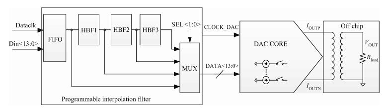
The block diagram of the proposed DAC is depicted in Fig. 1. It is mainly composed of a programmable digital interpolation filter and the DAC core. The programmable digital interpolation filter consists of a FIFO, three half-band filters (HBF1, HBF2 and HBF3) each with an interpolation factor of 2, and a MUX. The input signal to the DAC core (DATA < 13:0 > ) can have the same update rate as the input to the DAC (Din < 13:0 > ) or an update rate 2/4/8 times of the input to the DAC depending on the selection input SEL < 1:0 > to the MUX. The mode to be selected is determined by the DAC core update rate, and the programmable DAC works under non-interpolation mode, 2x-interpolation mode, 4x-interpolation mode or 8x-interpolation mode with the core update rate at 0–250 MS/s, 250–500 MS/s, 500–800 MS/s or 800–1000 GS/s, respectively.

Figure  1.  Block diagram of the proposed DAC.

For an interpolation filter with an interpolation factor of $I$, the output sequence $x_{I}(n)$ is:

$x_I (n)=\sum\limits_{m, =, 0}^N {h\left( {{\rm m}I+(n)_I } \right)} x\left( { {\frac{n}{I}}} \right),$

(1)

where $N$ is the filter order, $h(m)$ is the filter coefficient, and $x(n)$ is the input sequence. $I$ is 2 here as each half-band filter doubles the sampling rate.

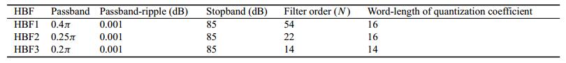
HBF1, HBF2 and HBF3 are half-band low-pass filters and because a half-band filter has 50 percent of its coefficients being zero, it outperforms other types in low power design. The filter order $N$ and the quantized coefficients can be obtained by using the MATLAB FDA tool. The performance of each half-band filter is listed in Table 1, and their frequency responses are plotted in Fig. 2.

Table  1.  Performance of each filter.
DownLoad: CSV  | Show Table
Figure  2.  Frequency response of (a) HBF1, (b) HBF2 and (c) HBF3.

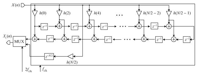
In the hardware implementation, several measures are taken to reduce the area and power consumption of the interpolation filters HBF1, HBF2 and HBF3. Firstly, the ploy-phase structure is adopted to reduce the hardware consumption, as shown in Fig. 3. Besides that, the filter is realized in transposed form which has the advantage of hardware reuse and also has the shortest critical path compared to other kinds of filter realization. Moreover, shift-and-add operations are used instead of dedicated multipliers to realize multiplication. Finally, a canonic sign digit (CSD) representation is adopted to express the coefficients. In this way, the coefficients can be represented with the fewest non-zero bits, which means minimal addition and subtraction operations.

Figure  3.  Block diagram of the interpolation filter HBF.

The block diagram of the DAC core is depicted in Fig. 4. The current-steering architecture adopted here is the best choice for fast-sampling DAC so far. In consideration of simplicity, compactness and reducing differential nonlinearity (DNL) and glitch energy, a 5-5-4 segmented structure is used, which consists of 5 thermometer coded most significant bits (5 MSB), 5 thermometer coded upper least significant bits (5 ULSB), and 4 binary coded lower least significant bits (4 LLSB). Most of the design effort is focused on the MSB and the ULSB as these two sections determine the overall performance of the DAC. As shown in Fig. 4, cells in the MSB and the ULSB are driven by row-and-column thermometer decoders, which are easy to design and area efficient. The input signal is separated into two channels (D and DB) with complementary clocks (CLK and CLKB), so signal D is half a clock before signal DB. Although it doubles the digital part area, the high-frequency performance will be greatly improved with a proper switching sequence.

Figure  4.  Block diagram of the DAC core.

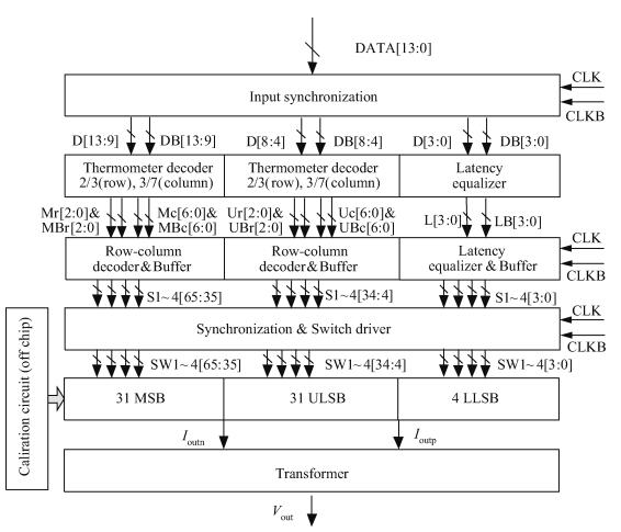
To meet the requirement of 2.5 V output amplitude, an off-chip transformer connects the DAC to the load. The impedance equals 100 $\Omega$ on both sides of the transformer, while the effective impedance to the DAC equals 50 $\Omega$.

A simple model for the current cell is shown in Fig. 5.

Figure  5.  Ideal switched current cell and simple model for analysis.

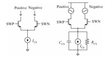
In this model, the current cell contains an ideal current cell and a pair of switches which determine the output current path and the differential voltage between the positive and negative output node. The major non-ideal effect of the current source is the finite frequency-dependent output impedance, which is modeled by $R_{\rm cs}$ and $C_{\rm cs}$ in Fig. 5. The spectral impurity of the DAC caused by the non-ideal current cell under different frequencies is discussed under this model.

Transistor mismatch of the current sources is a main source of nonlinearity. To meet the INL requirement of the DAC, the relationship between DAC INL_yield and the required accuracy on the current sources can be expressed as[5]:

$\frac{\sigma (I)}{I}\leqslant \frac{1}{\sqrt {2^N C}}, \quad C={\rm inv\_norm}\left(0.5+\frac{{\rm INL\_yield}}{2}\right),$

(2)

where $\sigma (I)/I$ is the relative standard deviation of a unit current source, $N$ is the resolution of the DAC, inv_norm is the reverse cumulative normal distribution and INL_yield is the relative number of DAC yield with INL < 0.5 LSB. A 14-bit converter with 99.7% yield specification at INL < 0.5 LSB requires a current error standard deviation of less than 0.125%. The minimal area of current cell can be expressed as:

$WL = \left[ {\frac{{4A_{{\rm{VT}}}^2}}{{{{\left( {{V_{{\rm{GS}}}} - {V_{{\rm{TH}}}}} \right)}^2}}} + A_\beta ^2} \right]/{\left( {\frac{{\sigma (I)}}{I}} \right)^2}_,$

(3)

in which $A_\beta$ and $A_{\rm VT}$ are technology parameter, $WL$ represents the area of the matched transistors, and $V_{\rm GS}-V_{\rm TH}$ is the gate overdrive voltage. According to Eqs. (2) and (3), the required area of the current sources can be determined.

The other factor that causes distortion at low frequency is the finite output impedance of DAC current cell $R_{\rm cs}$. As has been pointed out in other studies[6, 7], with the load resistor $R_{\rm load}$ and the total number of unit current sources $N$, the influence of the cell impedance $R_{\rm cs}$ on the third-order distortion of the converter can be described as:

${\rm HD}_3 =\left[R_{\rm load} N/ R_{\rm cs} \right]^2.$

(4)

From Eq. (4), it can be seen that the low frequency SFDR can be improved by increasing $R_{\rm cs}$. In order to improve the low frequency SFDR performance, the cascode current source structure is generally used.

Additional performance-degrading effects start to work when the sampling frequency gets high. An assumption of the output impedance can be modeled by the parallel connection of a resistor and a capacitor, and the expression for HD3 can be described as:

${\rm HD}_3 =\left[R_{\rm load} N/Z_{\rm cs} \right]^2.$

(5)

For the current sources of 5-bit MSB, to get HD$_{3}$ < –75 dB with a load resistance of 50 $\Omega$, $Z_{\rm cs}$ should be over 100 k$\Omega$, which is very difficult to reach at 1 GHz output frequency. Therefore, the output parasitic capacitance should be very small. For a cascode current source structure, the cascode transistors and switches need to be small to minimize parasitic capacitance.

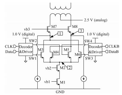
The cascode current source structure is adopted in this design as depicted in Fig. 6. The area of the current cell M1 is determined in a similar way to that described above and the cascode transistor M2 and the switches M3–M6 are minimized to reduce the high-frequency distortion. In addition, a fast switching method is used to reduce the parasitic capacitance[6].

Figure  6.  Current source structure.

Although a three-cascode-transistor structure can guarantee high impedance at low frequency, M7 and M8 could still cause large parasitic capacitance due to their large size. Therefore, two additional current paths are added to the sources of M7–M8, in which way these two transistors will not be completely switched off and the voltage of node 1 and node 3 will be much more stable. The parasitic capacitor $C_{\rm gs}$ of M7–M8 and $C_{\rm gd}$ of M3–M6 cannot be observed from the output node, and these capacitors will not contribute to distortion. The first observable capacitor due to switching is the capacitor $C_{\rm gs}$ of M3–M6, but their effect on finite output impedance will be reduced by the intrinsic gain of both M3–M6 and M7–M8 by a factor of ($g_{\rm m} r_{\rm out})$$^{2}$. The number of the current switches is four instead of two. Although they bring in more parasitic capacitors, it can improve high-frequency performance.

Any latch topology presents a load to the buffer that drives the clock input of the latch[8], which depends on whether the state of the latch is about to change or not. This effect will be significant when a large number of latches change with different states. It also becomes one of the most important limitations for high-frequency operation. So here, several circuits are implemented to minimize this effect.

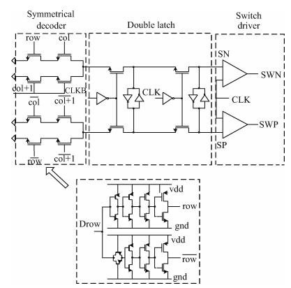
As mentioned in the DAC architecture, row-and-column decoders are used to reduce design complexity and save power. Furthermore, a symmetrical decoding method is adopted, as shown in Fig. 7 to minimize the decoding feed-through effect.

Figure  7.  Double latches with symmetrical decoding.

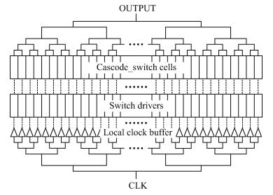
The latch shown in Fig. 7 is adopted to implement the synchronization of the switch-control signals, because it has the shortest clock-to-Q delay and the steepest transition. Although the transition of digital signals still has a finite settling effect at the end of the clock period, it is solved with the double-latch structure. To minimize the sensitivity of the driver to the data-dependent clock load, the clock is local buffered, thus it can enhance the strength of clock signal. Besides that, to minimize the intersymbol interference between successive input codes for achieving low distortion, the input data is also locally converted into a differential equivalent and buffered through a successively scaled buffer, as shown in Fig. 7, in which way it can also improve the switching speed.

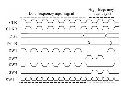
To further reduce the data-dependent clock loading effect, a four-switch method[9] is implemented as shown in Fig. 6 (M3–M6). In this method, two of the four switches change their states, while the other two remain off when the DAC is operating. The input data determines whether the output current flows to one output terminal or the other. It can be seen from Fig. 8 that regardless of whether the input signal is at low frequency or high frequency, the clock has the same load and node 2 in Fig. 6 suffers the same disturbances all the time.

Figure  8.  Current cell switch timing.

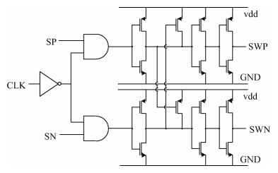
Meanwhile, the crossing point of the switch-control signals is also important. To prevent NMOS switch transistors from turning off at the same time, high crossing switch-control signals are needed, which are provided by the circuit shown in Fig. 9.

Figure  9.  Switch driver circuit.

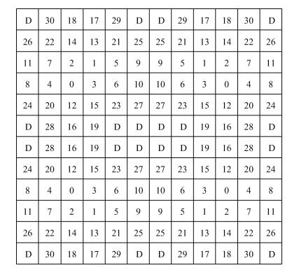
In the DAC design, the matching problem of the layout will have great influence on the chip performance when the DAC is fabricated. In order to ensure transistor-matching, a special layout technique called 'INL bounded switching sequences'[10] is adopted to cancel both the linear and quadratic gradient errors. The layout arrangement of the MSB and ULSB current sources is depicted in Fig. 10.

Figure  10.  Floor plan for MSB and ULSB current sources.

Another layout consideration is routing. According to Ref. [7], the delay differences caused by clock signal and output signal routing will degrade SFDR performance at high-speed operation. So a very tight control over relative timing is necessary. As shown in Fig. 11, binary tree routing method for the clock signal and output signal is adopted here.

Figure  11.  Clock signal and output signal routing.

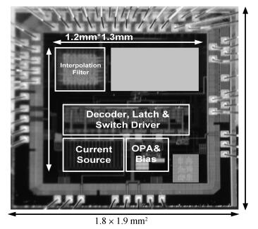
The DAC was fabricated in TSMC 65 nm CMOS technology. Figure 12 is the chip microphotograph, which shows that the core area is 1.2 $\times$ 1.3 mm$^{2}$. The measured DNL and INL plots are shown in Fig. 13 in which the measured DNL is $+$1.59 LSB/–1.26 LSB and the measured INL is $+$2.5 LSB/–1.06 LSB with off-chip calibration on. It can be seen that INL is not symmetrical. That is because current mirrors cause mismatch and the switching of full ULSB to MSB also causes mismatch. Getting ULSB through a current divider from MSB, instead of a current mirror, may achieve better performance.

Figure  12.  Microphotograph of the proposed DAC.
Figure  13.  DNL & INL.

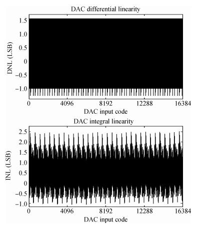
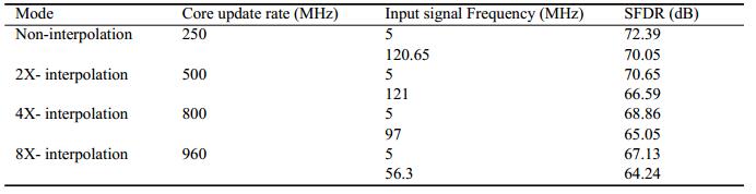
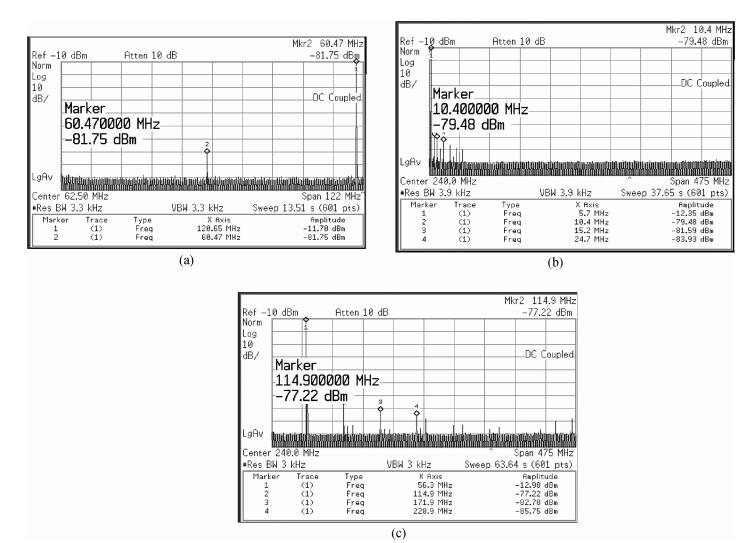
With the programmable digital interpolation filter, the DAC can work under 4 different modes, which are non-interpolation mode, 2x-interpolation mode, 4x-interpolation mode, and 8x-interpolation mode depending on the core update rate. Figure 14(a) shows that the measured SFDR is 70.05 dB for 120.65 MHz input signal when the update rate is 250 MS/s (non-interpolation mode). Under the 8x-interpolation mode, the output spectrum for 5 MHz input signal at 960 MS/s and 56.3 MHz input signal at 960 MS/s are shown in Figs. 14(b) and 14(c), and the SFDRs are 67.13 dB and 64.24 dB, respectively. As can be seen from Fig. 14, SFDR performance is limited by the second-order harmonic distortion. That is because fabrication will cause mismatch and layout and routing are not perfectly symmetrical. To minimize the effect, a better layout technique will be needed.

Figure  14.  Output spectra at (a) $f_{\rm sample}$ $=$ 250 MHz, $f_{\rm in}$ $=$ 120.65 MHz, (b) $f_{\rm sample}$ $=$ 960 MHz, $f_{\rm in}$ $=$ 5 MHz, and (c) $f_{\rm sample}$ $=$ 960 MHz, $f_{\rm in}$ $=$ 56.3 MHz.

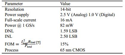
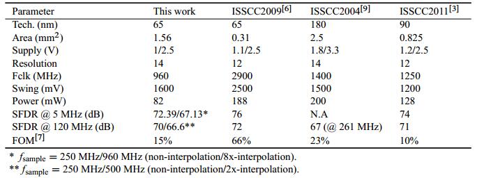
A summarized performance of the programmable DAC and a comparison between this work and other works are listed in Tables 2, 3 and 4. The analog part of the DAC consumes 42 mW from 2.5 V power supply while providing 16 mA full scale current and the digital part consumes 40 mW when the sampling frequency is 1 GHz.

Table  2.  DAC performance summary.
DownLoad: CSV  | Show Table
Table  3.  SFDR performance summary.
DownLoad: CSV  | Show Table
Table  4.  DAC performance comparison.
DownLoad: CSV  | Show Table

This paper presents a programmable 14-bit 1 GS/s DAC, which features a selectable interpolation rate (2x/4x/8x). A "fast switching" technique is adopted to reduce parasitic capacitance at high input frequency and the data-dependent clock loading effect is minimized by various methods such as symmetrical decoding, double-latch, local buffered clock and switch sequence control. The layout techniques for the current source transistors, the clock binary tree and the output signal binary tree are implemented to further improve SFDR at high frequency. The full-scale output current is 16 mA and the power consumption is 82 mW at 1 GS/s. The converter is designed in TSMC 65 nm technology and has a core area of 1.56 mm$^{2}$.


[1]
Huang Q, Francese P A, Martelli C, et al. A 200 MS/s 14 b 97 mW DAC in 0.18μm CMOS. ISSCC Dig Tech Papers, 2004:364 doi: 10.1007/978-3-642-31229-8_6/fulltext.html
[2]
Chan K L, Galton L. A 14 b 100 MS/s DAC with fully segmented dynamic element matching. ISSCC Dig Tech Papers, 2006:582
[3]
Tseng W H. A 12 b 1.25 GS/s DAC in 90 nm CMOS with >70 dB SFDR up to 500 MHz. ISSCC Dig Tech Papers, 2011:192 http://www.wenkuxiazai.com/doc/1ae59ba226fff705cd170a3f.html
[4]
Tseng W H, Wu J T, Chu Y C. A CMOS 8-bit 1.6-GS/s DAC with digital random return to zero. IEEE Trans Circuits Syst I, 2011, 58(1):1 doi: 10.1109/TCSI.2010.2097652
[5]
Van den Bosch A, Borremans M A F, Steyaert M S J, et al. A 10-ewpage bit 1-GSample/s Nyquist current-steering CMOS D/A converter. IEEE J Solid-State Circuits, 2001, 36(3):315 doi: 10.1109/4.910469
[6]
Lin C H, van der Goes F M L, Westra J R, et al. A 12 bit 2.9 GS/s DAC with IM3<-60 dBc beyond 1 GHz in 65 nm CMOS. IEEE J Solid-State Circuits, 2009, 44(12):3285 doi: 10.1109/JSSC.2009.2032624
[7]
Palimers P, Steyaert M S J. A 10-bit 1.6-GS/s 27-mW current-steering D/A converter with 550-MHz 54-dB SFDR bandwidth in 130-nm CMOS. IEEE Trans Circuits Syst I, 2010, 57(11):2870 doi: 10.1109/TCSI.2010.2052491
[8]
Mercer D A. Low-power approaches to high-speed current-steering digital-to-analog converters in 0.18μm CMOS. IEEE J Solid-State Circuits, 2007, 42(8):1688 doi: 10.1109/JSSC.2007.900279
[9]
Schafferer B, Adams R. A 3 V CMOS 400 mW 14 b 1.4 GS/s DAC for multi-carrier applications. ISSCC Dig Tech Papers, 2004:360 doi: 10.1007/978-3-642-31600-5_60
[10]
Cong Y, Geiger R L. Switching sequence optimization for gradient error compensation in thermometer-decoded DAC arrays. IEEE Trans Circuits Syst I, 2000, 47(7):589 http://www.oalib.com/paper/1520860
Fig. 1.  Block diagram of the proposed DAC.

Fig. 2.  Frequency response of (a) HBF1, (b) HBF2 and (c) HBF3.

Fig. 3.  Block diagram of the interpolation filter HBF.

Fig. 4.  Block diagram of the DAC core.

Fig. 5.  Ideal switched current cell and simple model for analysis.

Fig. 6.  Current source structure.

Fig. 7.  Double latches with symmetrical decoding.

Fig. 8.  Current cell switch timing.

Fig. 9.  Switch driver circuit.

Fig. 10.  Floor plan for MSB and ULSB current sources.

Fig. 11.  Clock signal and output signal routing.

Fig. 12.  Microphotograph of the proposed DAC.

Fig. 13.  DNL & INL.

Fig. 14.  Output spectra at (a) $f_{\rm sample}$ $=$ 250 MHz, $f_{\rm in}$ $=$ 120.65 MHz, (b) $f_{\rm sample}$ $=$ 960 MHz, $f_{\rm in}$ $=$ 5 MHz, and (c) $f_{\rm sample}$ $=$ 960 MHz, $f_{\rm in}$ $=$ 56.3 MHz.

Table 1.   Performance of each filter.

Table 2.   DAC performance summary.

Table 3.   SFDR performance summary.

Table 4.   DAC performance comparison.

[1]
Huang Q, Francese P A, Martelli C, et al. A 200 MS/s 14 b 97 mW DAC in 0.18μm CMOS. ISSCC Dig Tech Papers, 2004:364 doi: 10.1007/978-3-642-31229-8_6/fulltext.html
[2]
Chan K L, Galton L. A 14 b 100 MS/s DAC with fully segmented dynamic element matching. ISSCC Dig Tech Papers, 2006:582
[3]
Tseng W H. A 12 b 1.25 GS/s DAC in 90 nm CMOS with >70 dB SFDR up to 500 MHz. ISSCC Dig Tech Papers, 2011:192 http://www.wenkuxiazai.com/doc/1ae59ba226fff705cd170a3f.html
[4]
Tseng W H, Wu J T, Chu Y C. A CMOS 8-bit 1.6-GS/s DAC with digital random return to zero. IEEE Trans Circuits Syst I, 2011, 58(1):1 doi: 10.1109/TCSI.2010.2097652
[5]
Van den Bosch A, Borremans M A F, Steyaert M S J, et al. A 10-ewpage bit 1-GSample/s Nyquist current-steering CMOS D/A converter. IEEE J Solid-State Circuits, 2001, 36(3):315 doi: 10.1109/4.910469
[6]
Lin C H, van der Goes F M L, Westra J R, et al. A 12 bit 2.9 GS/s DAC with IM3<-60 dBc beyond 1 GHz in 65 nm CMOS. IEEE J Solid-State Circuits, 2009, 44(12):3285 doi: 10.1109/JSSC.2009.2032624
[7]
Palimers P, Steyaert M S J. A 10-bit 1.6-GS/s 27-mW current-steering D/A converter with 550-MHz 54-dB SFDR bandwidth in 130-nm CMOS. IEEE Trans Circuits Syst I, 2010, 57(11):2870 doi: 10.1109/TCSI.2010.2052491
[8]
Mercer D A. Low-power approaches to high-speed current-steering digital-to-analog converters in 0.18μm CMOS. IEEE J Solid-State Circuits, 2007, 42(8):1688 doi: 10.1109/JSSC.2007.900279
[9]
Schafferer B, Adams R. A 3 V CMOS 400 mW 14 b 1.4 GS/s DAC for multi-carrier applications. ISSCC Dig Tech Papers, 2004:360 doi: 10.1007/978-3-642-31600-5_60
[10]
Cong Y, Geiger R L. Switching sequence optimization for gradient error compensation in thermometer-decoded DAC arrays. IEEE Trans Circuits Syst I, 2000, 47(7):589 http://www.oalib.com/paper/1520860
1

Silicon-integrated high-speed mode and polarization switch-and-selector

Yihang Dong, Yong Zhang, Jian Shen, Zihan Xu, Xihua Zou, et al.

Journal of Semiconductors, 2022, 43(2): 022301. doi: 10.1088/1674-4926/43/2/022301

2

A survey of high-speed high-resolution current steering DACs

Xing Li, Lei Zhou

Journal of Semiconductors, 2020, 41(11): 111404. doi: 10.1088/1674-4926/41/11/111404

3

Study of the effect of switching speed of the a-SiC/c-Si (p)-based, thyristor-like, ultra-high-speed switches, using two-dimensional simulation techniques

Evangelos I. Dimitriadis, Nikolaos Georgoulas

Journal of Semiconductors, 2017, 38(5): 054001. doi: 10.1088/1674-4926/38/5/054001

4

High-resolution 1 MS/s sub-2 radix split-capacitor SAR ADC

Chao Cao, Zhangming Zhu

Journal of Semiconductors, 2017, 38(10): 105008. doi: 10.1088/1674-4926/38/10/105008

5

A CMOS high resolution, process/temperature variation tolerant RSSI for WIA-PA transceiver

Tao Yang, Yu Jiang, Jie Li, Jiangfei Guo, Hua Chen, et al.

Journal of Semiconductors, 2015, 36(8): 085005. doi: 10.1088/1674-4926/36/8/085005

6

A high-speed avalanche photodiode

Bin Li, Xiaohong Yang, Weihong Yin, Qianqian Lü, Rong Cui, et al.

Journal of Semiconductors, 2014, 35(7): 074009. doi: 10.1088/1674-4926/35/7/074009

7

A high speed low power low offset dynamic comparator used in SHA-less pipelined ADC

Shubin Liu, Zhangming Zhu, Yintang Yang, Lianxi Liu

Journal of Semiconductors, 2014, 35(5): 055008. doi: 10.1088/1674-4926/35/5/055008

8

The architecture design of a 2mW 18-bit high speed weight voltage type DAC based on dual weight resistance chain

Qixing Chen, Qiyu Luo

Journal of Semiconductors, 2013, 34(3): 035010. doi: 10.1088/1674-4926/34/3/035010

9

Robust design of a 500-MS/s 10-bit triple-channel current-steering DAC in 40 nm CMOS

Long Cheng, Yu Zhu, Kai Zhu, Chixiao Chen, Junyan Ren, et al.

Journal of Semiconductors, 2013, 34(10): 105007. doi: 10.1088/1674-4926/34/10/105007

10

A low-power high-speed driving circuit for spatial light modulators

Zhu Minghao, Zhu Congyi, Li Wenjiang, Zhang Yaohui

Journal of Semiconductors, 2012, 33(2): 025013. doi: 10.1088/1674-4926/33/2/025013

11

A current-steering self-calibration 14-bit 100-MSPs DAC

Qiu Dong, Fang Sheng, Li Ran, Xie Renzhong, Yi Ting, et al.

Journal of Semiconductors, 2010, 31(12): 125007. doi: 10.1088/1674-4926/31/12/125007

12

Design of high speed LVDS transceiver ICs

Xu Jian, Wang Zhigong, Niu Xiaokang

Journal of Semiconductors, 2010, 31(7): 075014. doi: 10.1088/1674-4926/31/7/075014

13

Ultra high-speed InP/InGaAs DHBTs with ft of 203 GHz

Su Yongbo, Jin Zhi, Cheng Wei, Liu Xinyu, Xu Anhuai, et al.

Journal of Semiconductors, 2009, 30(1): 014002. doi: 10.1088/1674-4926/30/1/014002

14

A direct digital frequency synthesizer with high-speed current-steering DAC

Yu Jinshan, Fu Dongbing, Li Ruzhang, Yao Yafeng, Yan Gang, et al.

Journal of Semiconductors, 2009, 30(10): 105006. doi: 10.1088/1674-4926/30/10/105006

15

A high speed direct digital frequency synthesizer realized by a segmented nonlinear DAC

Yuan Ling, Ni Weining, Hao Zhikun, Shi Yin, Li Wenchang, et al.

Journal of Semiconductors, 2009, 30(9): 095003. doi: 10.1088/1674-4926/30/9/095003

16

A high precision programmable bandgap voltage reference design for high resolution ADC

Zhu Tiancheng, Yao Suying, Li Binqiao

Journal of Semiconductors, 2009, 30(7): 075005. doi: 10.1088/1674-4926/30/7/075005

17

Multiplexer Design Applied to High-Speed Signal Transmission

Cao Hanmei, Yang Yintang, Cai Wei, Lu Tiejun, Wang Zongmin, et al.

Journal of Semiconductors, 2008, 29(6): 1040-1043.

18

Design of a High-Speed Low-Power 9-Port Register File

Cong Gaojian, Qi Jiayue

Chinese Journal of Semiconductors , 2007, 28(4): 614-618.

19

A High Speed,12-Channel Parallel,Monolithic IntegratedCMOS OEIC Receiver

Zhu Haobo, Mao Luhong, Yu Changliang, Chen Hongda, Tang Jun, et al.

Chinese Journal of Semiconductors , 2007, 28(9): 1341-1345.

20

High-Speed,Robust CMOS Dynamic Circuit Design

Lai Lianzhang, Tang Tingao, Lin Yinyin

Chinese Journal of Semiconductors , 2006, 27(6): 1006-1011.

  • Search

    Advanced Search >>

    GET CITATION

    Qi Zhao, Ran Li, Dong Qiu, Ting Yi, Yang Liu Bill, Zhiliang Hong. A 14-bit 1-GS/s DAC with a programmable interpolation filter in 65 nm CMOS[J]. Journal of Semiconductors, 2013, 34(2): 025004. doi: 10.1088/1674-4926/34/2/025004
    Q Zhao, R Li, D Qiu, T Yi, Y L Bill, Z L Hong. A 14-bit 1-GS/s DAC with a programmable interpolation filter in 65 nm CMOS[J]. J. Semicond., 2013, 34(2): 025004. doi: 10.1088/1674-4926/34/2/025004.
    shu

    Export: BibTex EndNote

    Article Metrics

    Article views: 2841 Times PDF downloads: 27 Times Cited by: 0 Times

    History

    Received: 19 June 2012 Revised: 06 September 2012 Online: Published: 01 February 2013

    Catalog

      Email This Article

      User name:
      Email:*请输入正确邮箱
      Code:*验证码错误
      Qi Zhao, Ran Li, Dong Qiu, Ting Yi, Yang Liu Bill, Zhiliang Hong. A 14-bit 1-GS/s DAC with a programmable interpolation filter in 65 nm CMOS[J]. Journal of Semiconductors, 2013, 34(2): 025004. doi: 10.1088/1674-4926/34/2/025004 ****Q Zhao, R Li, D Qiu, T Yi, Y L Bill, Z L Hong. A 14-bit 1-GS/s DAC with a programmable interpolation filter in 65 nm CMOS[J]. J. Semicond., 2013, 34(2): 025004. doi: 10.1088/1674-4926/34/2/025004.
      Citation:
      Qi Zhao, Ran Li, Dong Qiu, Ting Yi, Yang Liu Bill, Zhiliang Hong. A 14-bit 1-GS/s DAC with a programmable interpolation filter in 65 nm CMOS[J]. Journal of Semiconductors, 2013, 34(2): 025004. doi: 10.1088/1674-4926/34/2/025004 ****
      Q Zhao, R Li, D Qiu, T Yi, Y L Bill, Z L Hong. A 14-bit 1-GS/s DAC with a programmable interpolation filter in 65 nm CMOS[J]. J. Semicond., 2013, 34(2): 025004. doi: 10.1088/1674-4926/34/2/025004.

      A 14-bit 1-GS/s DAC with a programmable interpolation filter in 65 nm CMOS

      DOI: 10.1088/1674-4926/34/2/025004
      Funds:

      Project supported by the National High Technology Research and Development Program of China (No. 2009AA011605) and the National Natural Science Foundation of China (No. 61076027)

      the National Natural Science Foundation of China 61076027

      the National High Technology Research and Development Program of China 2009AA011605

      More Information
      • Corresponding author: Yi Ting, Email:yiting@fudan.edu.cn
      • Received Date: 2012-06-19
      • Revised Date: 2012-09-06
      • Published Date: 2013-02-01

      Catalog

        /

        DownLoad:  Full-Size Img  PowerPoint
        Return
        Return