


Fig1.
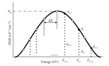
The discretization of deep Gaussian DOS for the analysis of the trap charge concentration.
SEMICONDUCTOR DEVICES
Corresponding author: Yao Ruohe,Email:gzu_jyuan@163.com
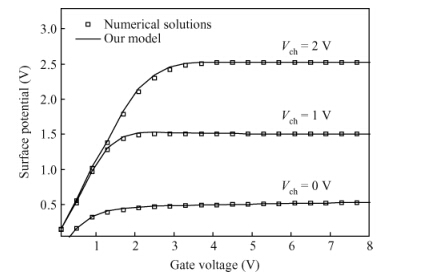
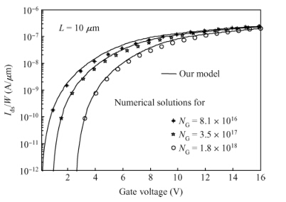
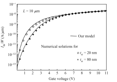
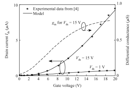
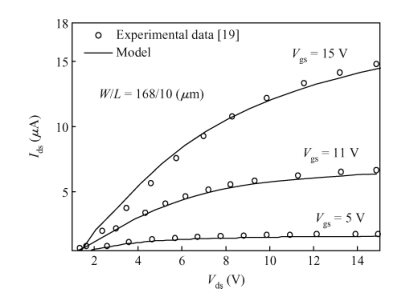
Abstract: Accounting for the deep Gaussian and tail exponential distribution of the density of states, a physical approximation for potentials of amorphous silicon thin-film transistors using a symmetric dual gate(sDG a-Si:H TFT) has been presented. The proposed scheme provides a complete solution of the potentials at the surface and center of the layer without solving any transcendental equations. A channel current model incorporating features of gate voltage-dependent mobility and coupling factor is derived. We show the parameters required for accurately describing the current-voltage(I-V) characteristics of DG a-Si:H TFT and just how sensitively these parameters affect TFT current. Particularly, the parameters' dependence on the I-V characteristics with respect to the density of deep state and channel thickness has been investigated in detail. The resulting scheme and model are successively verified through comparison with numerical simulations as well as the available experimental data.
Key words: amorphous silicon thin-film transistor, dual gate, surface potential, density of states, Gaussian deep states, drain current
| [1] | |
| [2] | |
| [3] | |
| [4] | |
| [5] | |
| [6] | |
| [7] | |
| [8] | |
| [9] | |
| [10] | |
| [11] | |
| [12] | |
| [13] | |
| [14] | |
| [15] | |
| [16] | |
| [17] | |
| [18] | |
| [19] | |
| [20] | |
| [21] | |
| [22] | |
| [23] | |
| [24] | |
| [25] | |
| [26] | |
| [27] | |
| [28] | |
| [29] |


Article views: 3766 Times PDF downloads: 23 Times Cited by: 0 Times
Received: 21 May 2015 Revised: Online: Published: 01 December 2015
| Citation: |
Jian Qin, Ruohe Yao. Modeling of current-voltage characteristics for dual-gate amorphous silicon thin-film transistors considering deep Gaussian density-of-state distribution[J]. Journal of Semiconductors, 2015, 36(12): 124005. doi: 10.1088/1674-4926/36/12/124005
****
J Qin, R H Yao. Modeling of current-voltage characteristics for dual-gate amorphous silicon thin-film transistors considering deep Gaussian density-of-state distribution[J]. J. Semicond., 2015, 36(12): 124005. doi: 10.1088/1674-4926/36/12/124005.

|
| [1] | |
| [2] | |
| [3] | |
| [4] | |
| [5] | |
| [6] | |
| [7] | |
| [8] | |
| [9] | |
| [10] | |
| [11] | |
| [12] | |
| [13] | |
| [14] | |
| [15] | |
| [16] | |
| [17] | |
| [18] | |
| [19] | |
| [20] | |
| [21] | |
| [22] | |
| [23] | |
| [24] | |
| [25] | |
| [26] | |
| [27] | |
| [28] | |
| [29] |

 WeChat ID
Journal of Semiconductors © 2017 All Rights Reserved 京ICP备05085259号-2

 DownLoad:


