Fig. 1.
(Color online) Timeline showing key development by polymer-assisted deposition. Metal oxides; metal nitrides; metal carbides; glassy-graphene; MoS2; MoS2/glassy-graphene heterostructure.
REVIEWS
Hongtao Ren1, 2, Yachao Liu1, Lei Zhang1, and Kai Liu2,
Corresponding author: Lei Zhang, Emails: zhangleio@xjtu.edu.cn; Kai Liu, Emails: liuk@tsinghua.edu.cn
Abstract: Two-dimensional (2D) materials have attracted considerable attention because of their novel and tunable electronic, optical, ferromagnetic, and chemical properties. Compared to mechanical exfoliation and chemical vapor deposition, polymer-assisted deposition (PAD) is more suitable for mass production of 2D materials owing to its good reproducibility and reliability. In this review, we summarize the recent development of PAD on syntheses of 2D materials. First, we introduce principles and processing steps of PAD. Second, 2D materials, including graphene, MoS2, and MoS2/glassy-graphene heterostructures, are presented to illustrate the power of PAD and provide readers with the opportunity to assess the method. Last, we discuss the future prospects and challenges in this research field. This review provides a novel technique for preparing 2D layered materials and may inspire new applications of 2D layered materials.
Keywords: polymer-assisted deposition, layered composite materials, glassy-graphene, MoS2, heterostructures
| [1] |
Jia Q X, McCleskey T M, Burrell A K, et al. Polymer-assisted deposition of metal-oxide films. Nat Mater, 2004, 3, 529 doi: 10.1038/nmat1163
|
| [2] |
Feng Q, Mao N, Wu J, et al. Growth of MoS2(1– x)Se2x (x = 0.41–1.00) monolayer alloys with controlled morphology by physical vapor deposition. ACS Nano, 2015, 9(7), 7450 doi: 10.1021/acsnano.5b02506
|
| [3] |
Feng Q, Zhu Y, Hong J, et al. Growth of large-area 2D MoS2(1– x)- Se2x semiconductor alloys. Adv Mater, 2014, 26(17), 2648 doi: 10.1002/adma.201306095
|
| [4] |
Hou J, Wang X, Fu D, et al. Modulating photoluminescence of monolayer molybdenum disulfide by metal-insulator phase transition in active substrates. Small, 2016, 12(29), 3976 doi: 10.1002/smll.v12.29
|
| [5] |
Kang K, Xie S, Huang L, et al. High-mobility three-atom-thick semiconducting films with wafer-scale homogeneity. Nature, 2015, 520, 656 doi: 10.1038/nature14417
|
| [6] |
Dumcenco D, Ovchinnikov D, Marinov K, et al. Large-area epitaxial monolayer MoS2. ACS Nano, 2015, 9(4), 4611 doi: 10.1021/acsnano.5b01281
|
| [7] |
Kochat V, Apte A, Hachtel J A, et al. Re doping in 2D transition metal dichalcogenides as a new route to tailor structural phases and induced magnetism. Adv Mater, 2017, 29(43), 1703754 doi: 10.1002/adma.201703754
|
| [8] |
Shukla P, Lin Y, Minogue E M, et al. Polymer assisted deposition (PAD) of thin metal films: A new technique to the preparation of metal oxides and reduced metal films. Actinides 2005-Basic Science, Applications and Technology, 2006, 893
|
| [9] |
Cao Y, Dai X, Zhang K, et al. One-step aqueous solution route toward depositing transparent carbon film onto different quartize substrate. Mater Lett, 2016, 185, 135 doi: 10.1016/j.matlet.2016.07.142
|
| [10] |
Bauer E, Mueller A H, Usov I, et al. Chemical solution route to conformal phosphor coatings on nanostructures. Adv Mater, 2008, 20(24), 4704 doi: 10.1002/adma.v20:24
|
| [11] |
Luo H, Wang H, Bi Z, et al. Highly conductive films of layered ternary transition-metal nitrides. Angew Chem Int Edit, 2009, 48(8), 1490 doi: 10.1002/anie.v48:8
|
| [12] |
Novoselov K S, Geim A K, Morozov S V, et al. Electric field effect in atomically thin carbon films. Science, 2004, 306(5696), 666 doi: 10.1126/science.1102896
|
| [13] |
Liu K, Wu J. Mechanical properties of two-dimensional materials and heterostructures. J Mater Res, 2015, 31(7), 832 doi: 10.1557/jmr.2015.324
|
| [14] |
Sun Y, Wang R, Liu K. Substrate induced changes in atomically thin 2-dimensional semiconductors: fundamentals, engineering, and applications. Appl Phys Rev, 2017, 4(1), 011301 doi: 10.1063/1.4974072
|
| [15] |
Yuan Z, Hou J, Liu K. Interfacing 2D semiconductors with functional oxides: fundamentals, properties, and applications. Crystals, 2017, 7(9), 265 doi: 10.3390/cryst7090265
|
| [16] |
Ren H, Xiong Z, Wang E, et al. Watching dynamic self-assembly of web buckles in strained MoS2 thin films. ACS Nano, 2019, 13, 3106 doi: 10.1021/acsnano.8b08411
|
| [17] |
Sun Y, Liu K. Strain engineering in functional 2-dimensional materials. J Appl Phys, 2019, 125(8), 082402 doi: 10.1063/1.5053795
|
| [18] |
Sun Y, Pan J, Zhang Z, et al. Elastic properties and fracture behaviors of biaxially deformed, polymorphic MoTe2. Nano Lett, 2019, 19(2), 761 doi: 10.1021/acs.nanolett.8b03833
|
| [19] |
Wang X, Fan W, Fan Z, et al. Substrate modified thermal stability of mono- and few-layer MoS2. Nanoscale, 2018, 10(7), 3540 doi: 10.1039/C7NR08941D
|
| [20] |
Hong S, Fu D, Hou J, et al. Robust photoluminescence energy of MoS2/graphene heterostructure against electron irradiation. Sci China Mater, 2018, 61(2095–8226), 1351 doi: 10.1007/s40843-018-9255-9
|
| [21] |
Lin Y, Xie J, Wang H, et al. Green luminescent zinc oxide films prepared by polymer-assisted deposition with rapid thermal process. Thin Solid Films, 2005, 492(1/2), 101 doi: 10.1016/j.tsf.2005.06.060
|
| [22] |
Ren H, Xiang G, Gu G, et al. Zinc vacancy-induced room-temperature ferromagnetism in undoped ZnO thin films. J Nanomater, 2012, 6, 295358 doi: 10.1155/2012/295358
|
| [23] |
Ren H, Xiang G, Gu G, et al. Enhancement of ferromagnetism of ZnO:Co nanocrystals by post-annealing treatment: The role of oxygen interstitials and zinc vacancies. Mater Lett, 2014, 122, 256 doi: 10.1016/j.matlet.2014.02.063
|
| [24] |
Ren H, Xiang G, Luo J, et al. Direct catalyst-free self-assembly of large area of horizontal ferromagnetic ZnO nanowire arrays. Mater Lett, 2019, 234, 384 doi: 10.1016/j.matlet.2018.09.145
|
| [25] |
Luo H, Lin Y, Wang H, et al. Epitaxial GaN thin films prepared by polymer-assisted deposition. J Phys Chem C, 2008, 112(51), 20535 doi: 10.1021/jp807793p
|
| [26] |
Zou G, Jain M, Zhou H, et al. Ultrathin epitaxial superconducting niobium nitride films grown by a chemical solution technique. Chem Commun, 2008(45), 6022 doi: 10.1039/b815066d
|
| [27] |
Luo H, Wang H, Bi Z, et al. Epitaxial ternary nitride thin films prepared by a chemical solution method. J Am Chem Soc, 2008, 130(46), 15224 doi: 10.1021/ja803544c
|
| [28] |
Luo H, Lin Y, Wang H, et al. A chemical solution approach to epitaxial metal nitride thin films. Adv Mater, 2009, 21(2), 193 doi: 10.1002/adma.v21:2
|
| [29] |
Luo H, Zou G, Wang H, et al. Controlling crystal structure and oxidation state in molybdenum nitrides through epitaxial stabilization. J Phys Chem C, 2011, 115(36), 17880 doi: 10.1021/jp2048376
|
| [30] |
Zhang Y, Haberkorn N, Ronning F, et al. Epitaxial superconducting delta-MoN films grown by a chemical solution method. J Am Chem Soc, 2011, 133(51), 20735 doi: 10.1021/ja208868k
|
| [31] |
Haberkorn N, Zhang Y Y, Kim J, et al. Upper critical magnetic field and vortex-free state in very thin epitaxial delta-MoN films grown by polymer-assisted deposition. Supercond Sci Tech, 2013, 26(10), 105023 doi: 10.1088/0953-2048/26/10/105023
|
| [32] |
Pan T S, Zhang Y, Huang J, et al. Particle size effect on thermal conductivity of AlN films with embedded diamond particles. Appl Phys A, 2014, 114(3), 973 doi: 10.1007/s00339-013-8045-0
|
| [33] |
Zou G, Wang H, Mara N, et al. Chemical solution deposition of epitaxial carbide films. J Am Chem Soc, 2010, 132(8), 2516 doi: 10.1021/ja9102315
|
| [34] |
Zou G, Luo H, Zhang Y, et al. A chemical solution approach for superconducting and hard epitaxial NbC film. Chem Commun, 2010, 46(41), 7837 doi: 10.1039/c0cc01295e
|
| [35] |
Yi Q, Dai X, Zhao J, et al. Enhanced mechanical strength and electrical conductivity of carbon-nanotube/TiC hybrid fibers. Nanoscale, 2013, 5(15), 6923 doi: 10.1039/c3nr01857a
|
| [36] |
Zou G F, Luo H M, Ronning F, et al. Facile chemical solution deposition of high-mobility epitaxial germanium films on silicon. Angew Chem Int Edit, 2010, 49(10), 1782 doi: 10.1002/anie.v49:10
|
| [37] |
Dai X, Wu J, Qian Z, et al. Ultra-smooth glassy graphene thin films for flexible transparent circuits. Sci Adv, 2016, 2(11), e1601574 doi: 10.1126/sciadv.1601574
|
| [38] |
Xu H, Han X, Dai X, et al. High detectivity and transparent few-layer MoS2/glassy-graphene heterostructure photodetectors. Adv Mater, 2018, 30(13), e1706561 doi: 10.1002/adma.201706561
|
| [39] |
Yang H, Giri A, Moon S, et al. Highly scalable synthesis of MoS2 thin films with precise thickness control via polymer-assisted deposition. Chem Mater, 2017, 29(14), 5772 doi: 10.1021/acs.chemmater.7b01605
|
| [40] |
Zhu J T, Wu J, Sun Y H, et al. Thickness-dependent bandgap tunable molybdenum disulfide films for optoelectronics. Rsc Adv, 2016, 6(112), 110604 doi: 10.1039/C6RA22496B
|
| [41] |
Lin Y, Wang H, Hawley M E, et al. Epitaxial growth of Eu2O3 thin films on LaAlO3 substrates by polymer-assisted deposition. Appl Phys Lett, 2004, 85(16), 3426 doi: 10.1063/1.1806265
|
| [42] |
Garcia M A, Ali M N, Parsons-Moss T, et al. Metal oxide films produced by polymer-assisted deposition (PAD) for nuclear science applications. Thin Solid Films, 2008, 516(18), 6261 doi: 10.1016/j.tsf.2007.11.127
|
| [43] |
Ali M N, Garcia M A, Parsons-Moss T, et al. Polymer-assisted deposition of homogeneous metal oxide films to produce nuclear targets. Nat Protoc, 2010, 5(8), 1440 doi: 10.1038/nprot.2010.105
|
| [44] |
Garcia M A, Ali M N, Chang N N, et al. Metal oxide targets produced by the polymer-assisted deposition method. Nucl Instrum Meth A, 2010, 613(3), 396 doi: 10.1016/j.nima.2009.09.084
|
| [45] |
Jain M, Shukla P, Li Y, et al. Manipulating magnetoresistance near room temperature in La0.67Sr0.33MnO3/La0.67Ca0.33MnO3 films prepared by polymer assisted deposition. Adv Mater, 2006, 18(20), 2695 doi: 10.1002/(ISSN)1521-4095
|
| [46] |
McCleskey T M, Bauer E, Jia Q, et al. Optical band gap of NpO2 and PuO2 from optical absorbance of epitaxial films. J Appl Phys, 2013, 113(1), 013515 doi: 10.1063/1.4772595
|
| [47] |
Wen X D, Loeble M W, Batista E R, et al. Electronic structure and O K-edge XAS spectroscopy of U3O8. J Electron Spectrosc, 2014, 194, 81 doi: 10.1016/j.elspec.2014.03.005
|
| [48] |
Jain M, Li Y, Hundley M F, et al. Magnetoresistance in polymer-assisted deposited Sr- and Ca-doped lanthanum manganite films. Appl Phys Lett, 2006, 88(23), 232510 doi: 10.1063/1.2207497
|
| [49] |
Luo H M, Jain M, Baily S A, et al. Structural and ferromagnetic properties of epitaxial SrRuO3 thin films obtained by polymer-assisted deposition. J Phys Chem B, 2007, 111(26), 7497 doi: 10.1021/jp0718451
|
| [50] |
Jain M, Lin Y, Shukla P, et al. Ferroic metal-oxide films grown by polymer assisted deposition. Thin Solid Films, 2007, 515(16), 6411 doi: 10.1016/j.tsf.2006.11.144
|
| [51] |
Luo H, Yang H, Bally S A, et al. Self-assembled epitaxial nanocomposite BaTiO3–NiFe2O4 films prepared by polymer-assisted deposition. J Am Chem Soc, 2007, 129(46), 14132 doi: 10.1021/ja075764u
|
| [52] |
Jain M, Bauer E, Lin Y, et al. BaTiO3-related ferroelectric thin fflms by polymer assisted deposition. Integr Ferroelectr, 2008, 100, 132 doi: 10.1080/10584580802540645
|
| [53] |
Lucas I, Vila-Fungueirino J M, Jimenez-Cavero P, et al. Tunnel conduction in epitaxial bilayers of ferromagnetic LaCoO3/La2/3Sr1/3MnO3 deposited by a chemical solution method. ACS Appl Mater Inter, 2014, 6(23), 21279 doi: 10.1021/am506259p
|
| [54] |
Yi Q, Wang H, Cong S, et al. Self-cleaning glass of photocatalytic anatase TiO2@carbon nanotubes thin film by polymer-assisted approach. Nanoscale Res Lett, 2016, 11, 457 doi: 10.1186/s11671-016-1674-4
|
| [55] |
Shukla P, Minogue E M, McCleskey T M, et al. Conformal coating of nanoscale features of microporous AnodiscTM membranes with zirconium and titanium oxides. Chem Commun, 2006(8), 847 doi: 10.1039/b513410b
|
| [56] |
Gillman E S, Costello D, Moreno M, et al. Polymer-assisted conformal coating of TiO2 thin films. J Appl Phys, 2010, 108(4), 044310 doi: 10.1063/1.3443574
|
| [57] |
Lin Y, Zeng B, Ji Y, et al. Nucleation dynamics of nanostructural TiO2 films with controllable phases on (001) LaAlO3. Nanotechnology, 2014, 25(1), 014014 doi: 10.1088/0957-4484/25/1/014014
|
| [58] |
Yi Q H, Cong S, Wang H, et al. High-stability Ti4+ precursor for the TiO2 compact layer of dye-sensitized solar cells. Appl Surf Sci, 2015, 356, 587 doi: 10.1016/j.apsusc.2015.08.050
|
| [59] |
Ji Y, Zhang Y, Gao M, et al. Role of microstructures on the M1–M2 phase transition in epitaxial VO2 thin films. Sci Rep-UK, 2014, 4, 4854 doi: 10.1038/srep04854
|
| [60] |
Ji Y, Zhang Y, Gao M, et al. Growth and physical properties of vanadium oxide thin films with controllable phases. MRS Proceedings, 2013, 1547, 21
|
| [61] |
Yue F, Huang W, Shi Q, et al. Phase transition properties of vanadium oxide films deposited by polymer-assisted deposition. J Sol-Gel Sci Techn, 2014, 72(3), 565 doi: 10.1007/s10971-014-3474-6
|
| [62] |
Breckenfeld E, Kim H, Gorzkowski E P, et al. Laser-processing of VO2 thin films synthesized by polymer-assisted-deposition. Appl Surf Sci, 2017, 397, 152 doi: 10.1016/j.apsusc.2016.11.113
|
| [63] |
Gao M, Qi Z, Lu C, et al. Interplay between extra charge injection and lattice evolution in VO2/CH3NH3 PbI3 heterostructure. Phys Status Solidi R, 2018, 1700416 doi: 10.1002/pssr.201700416
|
| [64] |
Liang W, Gao M, Lu C, et al. Enhanced metal-insulator transition performance in scalable vanadium dioxide thin films prepared using a moisture-assisted chemical solution approach. ACS Appl Mater Inter, 2018, 10(9), 8341 doi: 10.1021/acsami.7b18533
|
| [65] |
Lin Y, Lee J S, Wang H, et al. Structural and dielectric properties of epitaxial Ba1−xSrxTiO3 films grown on LaAlO3 substrates by polymer-assisted deposition. Appl Phys Lett, 2004, 85(21), 5007 doi: 10.1063/1.1827927
|
| [66] |
Jain M, Bauer E, Ronning F, et al. Mixed-valence perovskite thin films by polymer-assisted deposition. J Am Ceram Soc, 2008, 91(6), 1858 doi: 10.1111/j.1551-2916.2008.02396.x
|
| [67] |
Yao G, Ji Y, Liang W, et al. Influence of the vicinal surface on the anisotropic dielectric properties of highly epitaxial Ba0.7Sr0.3TiO3 thin films. Nanoscale, 2017, 9(9), 3068 doi: 10.1039/C6NR09044C
|
| [68] |
Luo H, Jain M, McCleskey T M, et al. Optical and structural properties of single phase epitaxial p-type transparent oxide thin films. Adv Mater, 2007, 19(21), 3604 doi: 10.1002/adma.200700528
|
| [69] |
Luo H, Mueller A H, McCleskey T M, et al. Structural and photoelectrochemical properties of BiVO4 thin films. J Phys Chem C, 2008, 112(15), 6099 doi: 10.1021/jp7113187
|
| [70] |
Xu Y, Chen G, Fu E, et al. Nickel substituted LiMn2O4 cathode with durable high-rate capability for Li-ion batteries. Rsc Adv, 2013, 3(40), 18441 doi: 10.1039/c3ra42223b
|
| [71] |
Yuan C Z, Li J Y, Hou L R, et al. Polymer-assisted synthesis of a 3D hierarchical porous network-like spinel NiCo2O4 framework towards high-performance electrochemical capacitors. J Mater Chem A, 2013, 1(37), 11145 doi: 10.1039/c3ta11949a
|
| [72] |
Mos R B, Petrisor T Jr, Nasui M, et al. Enhanced structural and morphological properties of Gd-doped CeO2 thin films obtained by polymer-assisted deposition. Mater Lett, 2014, 124, 306 doi: 10.1016/j.matlet.2014.03.119
|
| [73] |
Chuai Y H, Shen H Z, Li Y, et al. Epitaxial growth of highly infrared-transparent and conductive CuScO2 thin film by polymer-assisted-deposition method. Rsc Adv, 2015, 5(61), 49301 doi: 10.1039/C5RA07743E
|
| [74] |
Lin Y, Feng D Y, Gao M, et al. Reducing dielectric loss in CaCu3Ti4O12 thin films by high-pressure oxygen annealing. J Mater Chem C, 2015, 3(14), 3438 doi: 10.1039/C5TC00197H
|
| [75] |
Gao M, Feng D, Yao G, et al. Chemical and mechanical strains tuned dielectric properties in Zr-doped CaCu3Ti4O12 highly epitaxial thin films. Rsc Adv, 2015, 5(113), 92958 doi: 10.1039/C5RA18149F
|
| [76] |
Xie C, Shi L, Zhou S, et al. Structural characteristics, magnetic properties of Re2NiMnO6 (Re = La, Pr, Nd, Sm, Y) thin films on (001) LaAlO3 by simple polymer assisted deposition. Surf Coat Tech, 2015, 277, 222 doi: 10.1016/j.surfcoat.2015.07.056
|
| [77] |
Yao D, Shi L, Zhou S, et al. Tuning the metal–insulator transition via epitaxial strain and Co doping in NdNiO3 thin films grown by polymer-assisted deposition. J Appl Phys, 2016, 119(3), 035303 doi: 10.1063/1.4940393
|
| [78] |
Chuai Y, Wang X, Zheng C, et al. Highly infrared-transparent and p-type conductive CuSc(1– x)Sn( x)O2 thin films and a p-CuScO2: Sn/n-ZnO heterojunction fabricated by the polymer-assisted deposition method. Rsc Adv, 2016, 6(38), 31726 doi: 10.1039/C6RA00919K
|
| [79] |
Lei M, Zhang Y, Zhao Y. Coating conditions of SCO single buffer layer via Slot-Die technique. IEEE T Appl Supercon, 2016, 26(3), 1 doi: 10.1109/tasc.2016.2542271
|
| [80] |
Lucas I, Jiménez-Cavero P, Vila-Fungueiriño J M, et al. Chemical solution synthesis and ferromagnetic resonance of epitaxial thin films of yttrium iron garnet. Phys Rev Mater, 2017, 1(7), 074407 doi: 10.1103/PhysRevMaterials.1.074407
|
| [81] |
Scott B L, Joyce J J, Durakiewicz T D, et al. High quality epitaxial thin films of actinide oxides, carbides, and nitrides: Advancing understanding of electronic structure of f-element materials. Coordin Chem Rev, 2014, 266, 137 doi: 10.1016/j.ccr.2013.09.019
|
| [82] |
Jilek R E, Bauer E, Burrell A K, et al. Preparation of epitaxial uranium dicarbide thin films by polymer-assisted deposition. Chem Mater, 2013, 25(21), 4373 doi: 10.1021/cm402655p
|
| [83] |
Elbaz L, Kreller C R, Henson N J, et al. Electrocatalysis of oxygen reduction with platinum supported on molybdenum carbide-carbon composite. J Electroanal Chem, 2014, 720, 34 doi: 10.1016/j.jelechem.2014.02.023
|
| [84] |
Cobas R, Muñoz-Perez S, Cadogan J M, et al. Magnetoresistance in epitaxial thin films of La0.85Ag0.15MnO3 produced by polymer assisted deposition. Appl Phys Lett, 2011, 99(8), 083113 doi: 10.1063/1.3629993
|
| [85] |
Kim Y Y, Hwang J S, Kim J K, et al. Electrical and optical properties of hydrogen plasma treated molybdenum doped indium oxide films synthesized by polymer-assisted deposition method. Ceram Int, 2017, 43, S506 doi: 10.1016/j.ceramint.2017.05.256
|
| [86] |
Yi Q, Wu J, Zhao J, et al. Tuning bandgap of p-type Cu2Zn(Sn, Ge)(S, Se)4 semiconductor thin films via aqueous polymer-assisted deposition. ACS Appl Mater Inter, 2017, 9(2), 1602 doi: 10.1021/acsami.6b13683
|
| [87] |
Hong S J, Jun H, Lee J S. Nanocrystalline WO3 film with high photo-electrochemical activity prepared by polymer-assisted direct deposition. Scripta Mater, 2010, 63(7), 757 doi: 10.1016/j.scriptamat.2010.05.021
|
| [88] |
Luo H, Lin Y, Wang H, et al. Amorphous silica nanoparticles embedded in epitaxial SrTiO3 and CoFe2O4 matrices. Angew Chem Int Edit, 2008, 47(31), 5768 doi: 10.1002/anie.v47:31
|
| [89] |
Burrell A K, McCleskey T M, Shukla P, et al. Controlling oxidation states in uranium oxides through epitaxial stabilization. Adv Mater, 2007, 19(21), 3559 doi: 10.1002/adma.200701157
|
| [90] |
Vishwanath S K, An T, Jin W Y, et al. The optoelectronic properties of tungsten-doped indium oxide thin films prepared by polymer-assisted solution processing for use in organic solar cells. J Mater Chem C, 2017, 5(39), 10295 doi: 10.1039/C7TC03662K
|
| [91] |
Hwang J S, Lee J M, Vishwanath S K, et al. Effects of H2 plasma treatment on the electrical properties of titanium-doped indium oxide films prepared by polymer-assisted deposition. J Vac Sci Technol A, 2015, 33(4), 041402 doi: 10.1116/1.4922289
|
| [92] |
Tao L, Chen K, Chen Z, et al. Centimeter-scale CVD growth of highly crystalline single-layer MoS2 film with spatial homogeneity and the visualization of grain boundaries. ACS Appl Mater Inter, 2017, 9(13), 12073 doi: 10.1021/acsami.7b00420
|
| [93] |
Jurca T, Moody M J, Henning A, et al. Low-temperature atomic layer deposition of MoS2 films. Angew Chem Int Edit, 2017, 56(18), 4991 doi: 10.1002/anie.201611838
|
| [94] |
Shi Y, Zhou Y, Yang D R, et al. Energy level engineering of MoS2 by transition-metal doping for accelerating hydrogen evolution reaction. J Am Chem Soc, 2017, 139(43), 15479 doi: 10.1021/jacs.7b08881
|
| [95] |
Suh J, Tan T L, Zhao W, et al. Reconfiguring crystal and electronic structures of MoS2 by substitutional doping. Nat Commun, 2018, 9(1), 199 doi: 10.1038/s41467-017-02631-9
|
| [96] |
Tan H, Hu W, Wang C, et al. Intrinsic ferromagnetism in Mn-substituted MoS2 nanosheets achieved by supercritical hydrothermal reaction. Small, 2017, 13(39), 1701389 doi: 10.1002/smll.v13.39
|
| [97] |
Xiang Z, Zhang Z, Xu X, et al. Room-temperature ferromagnetism in Co doped MoS2 sheets. Phys Chem Chem Phys, 2015, 17(24), 15822 doi: 10.1039/C5CP01509J
|
| [98] |
Cheng Y C, Zhu Z Y, Mi W B, et al. Prediction of two-dimensional diluted magnetic semiconductors: Doped monolayer MoS2 systems. Phys Rev B, 2013, 87(10), 100401 doi: 10.1103/PhysRevB.87.100401
|
| [99] |
Liu G, Robertson A W, Li M M, et al. MoS2 monolayer catalyst doped with isolated Co atoms for the hydrodeoxygenation reaction. Nat Chem, 2017, 9(8), 810 doi: 10.1038/nchem.2740
|
| [100] |
Li B, Xing T, Zhong M Z, et al. A two-dimensional Fe-doped SnS2 magnetic semiconductor. Nat Commun, 2017, 8, 1958 doi: 10.1038/s41467-017-02077-z
|
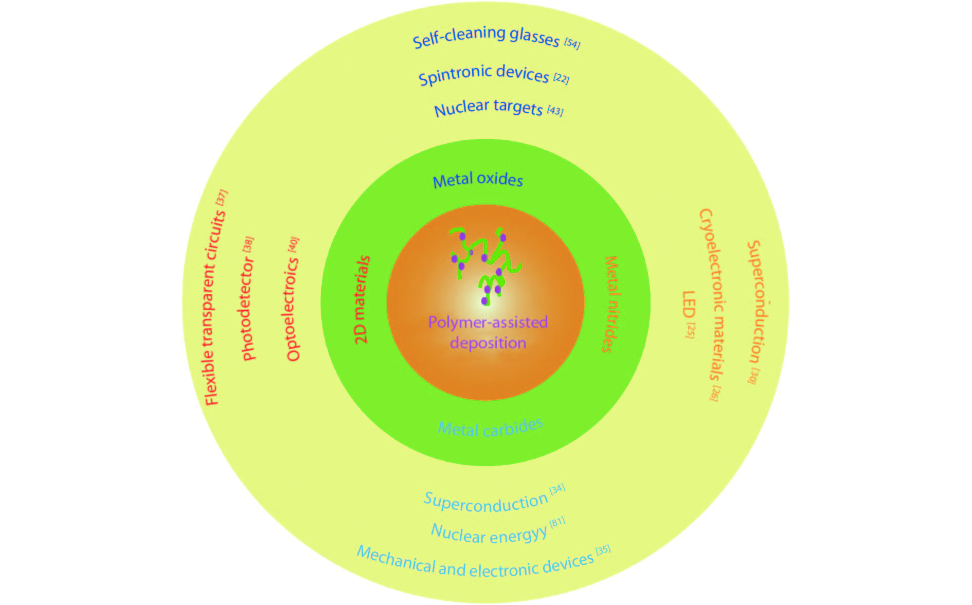
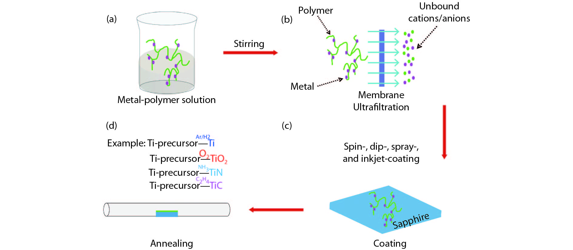
Table 1. Elements in the magenta boxes coordinated with polymer to form a stable complex. The elements shown in red font were bound with the polymer in the previous reports.
 |
 DownLoad: CSV
Table 2. Summary of various metal elements binded by polymers.
| Element | Metal precursor | Polymer | Element | Metal precursor | Polymer |
| Li[70] | LiNO3 | PEI + EDTA | Ru[49] | RuCl3 | PAA |
| C[37] | C6H12O6 | PEI | Ag[84] | AgNO3 | PEI + C6H8O7 |
| Al[68] | Al(NO3)3 | PEI + HF | In[85] | In(NO3)3 | PEI |
| Ca[45] | Ca(OH)2 | PEI | Sn[86] | SnCl2 | PEIC |
| Sc[73] | Sc(NO3)3 | PEI + EDTA | Ba[65] | Ba(NO3)2 | PEI + EDTA |
| Ti[1] | Ti(cat)3(NH4)2 | PEI | Hf[42] | HfCl4 | PEI |
| V [10] | VOSO4 | PEI + EDTA | Ta[33] | TaCl5 | PEI + HF |
| Mn[45] | MnCl2 | PEI + EDTA | W[87] | (NH4)2WO4 | PEI |
| Fe[88] | FeCl3 | PEI | Bi[10] | Bi(NO3)3 | PEI + EDTA |
| Co[88] | CoCl2 | PEI | La[45] | La(NO3)3 | PEI + EDTA |
| Ni[51] | Ni(NO3)2 | PEI + EDTA | Ce[72] | Ce(NO3)3 | PEI + EDTA |
| Cu[68] | Cu(NO3)2 | PEI | Pr[76] | Pr(NO3)3 | PEI + EDTA |
| Zn[22] | Zn(NO3)2 | PEI | Nd[76] | Nd(NO3)3 | PEI + EDTA |
| Ga[25] | GaCl5 | PEI | Sm[76] | Sm(NO3)3 | PEI + EDTA |
| Ge[36] | GeO2 | PEI + EDTA | Eu[42] | EuCl3 | PEI |
| Sr[1] | Sr(NO3)2 | PEI + EDTA | Gd[72] | Gd(NO3)3 | PEI + EDTA |
| Y[10] | Y(NO3)3 | PEI + EDTA | Tm[42] | TmCl3 | PEI |
| Zr[55] | ZrO(NO3)2 | PEI + EDTA | U[89] | UO2(oAc)2 | PEI |
| Nb[26] | NbCl5 | PEI + HF | Np[46] | 239Np solution | PEI + EDTA |
| Mo[16] | (NH4)6Mo7O24 | PEI + EDTA | Pu[46] | 239Pu solution | PEI + EDTA |
DownLoad: CSV
Table 3. Comparison of three different methods to synthesize MoS2 and MoS2 field-effect transistor structures.
| Method | Precursor gas | Temperature (°C) | Crystalization | Conformal | Size | Mobility (cm2/(V·s)) | Response time | Ion/Ioff ratio |
| CVD | Ar | 1000 | Single-crystal | No | ~cm2 | 9.6 | – | 105[92] |
| Ar | 850 | Single-crystal | No | – | 50 | – | 106[92] | |
| ALD | H2S; Ar | 60 | Amorphous | Yes | – | 0.23 | – | 102[93] |
| PAD | Ar + H2 | 850 | Polycrystalline | Yes | ~cm2 | – | 0.3 ms | 3[40] |
| Ar + H2 | 700 | Polycrystalline | Yes | 6-inch | – | 1.0 ms | 104[39] | |
| Ar + H2 | 550 | Amorphous | Yes | ~cm2 | – | – | –[16] |
DownLoad: CSV
| [1] |
Jia Q X, McCleskey T M, Burrell A K, et al. Polymer-assisted deposition of metal-oxide films. Nat Mater, 2004, 3, 529 doi: 10.1038/nmat1163
|
| [2] |
Feng Q, Mao N, Wu J, et al. Growth of MoS2(1– x)Se2x (x = 0.41–1.00) monolayer alloys with controlled morphology by physical vapor deposition. ACS Nano, 2015, 9(7), 7450 doi: 10.1021/acsnano.5b02506
|
| [3] |
Feng Q, Zhu Y, Hong J, et al. Growth of large-area 2D MoS2(1– x)- Se2x semiconductor alloys. Adv Mater, 2014, 26(17), 2648 doi: 10.1002/adma.201306095
|
| [4] |
Hou J, Wang X, Fu D, et al. Modulating photoluminescence of monolayer molybdenum disulfide by metal-insulator phase transition in active substrates. Small, 2016, 12(29), 3976 doi: 10.1002/smll.v12.29
|
| [5] |
Kang K, Xie S, Huang L, et al. High-mobility three-atom-thick semiconducting films with wafer-scale homogeneity. Nature, 2015, 520, 656 doi: 10.1038/nature14417
|
| [6] |
Dumcenco D, Ovchinnikov D, Marinov K, et al. Large-area epitaxial monolayer MoS2. ACS Nano, 2015, 9(4), 4611 doi: 10.1021/acsnano.5b01281
|
| [7] |
Kochat V, Apte A, Hachtel J A, et al. Re doping in 2D transition metal dichalcogenides as a new route to tailor structural phases and induced magnetism. Adv Mater, 2017, 29(43), 1703754 doi: 10.1002/adma.201703754
|
| [8] |
Shukla P, Lin Y, Minogue E M, et al. Polymer assisted deposition (PAD) of thin metal films: A new technique to the preparation of metal oxides and reduced metal films. Actinides 2005-Basic Science, Applications and Technology, 2006, 893
|
| [9] |
Cao Y, Dai X, Zhang K, et al. One-step aqueous solution route toward depositing transparent carbon film onto different quartize substrate. Mater Lett, 2016, 185, 135 doi: 10.1016/j.matlet.2016.07.142
|
| [10] |
Bauer E, Mueller A H, Usov I, et al. Chemical solution route to conformal phosphor coatings on nanostructures. Adv Mater, 2008, 20(24), 4704 doi: 10.1002/adma.v20:24
|
| [11] |
Luo H, Wang H, Bi Z, et al. Highly conductive films of layered ternary transition-metal nitrides. Angew Chem Int Edit, 2009, 48(8), 1490 doi: 10.1002/anie.v48:8
|
| [12] |
Novoselov K S, Geim A K, Morozov S V, et al. Electric field effect in atomically thin carbon films. Science, 2004, 306(5696), 666 doi: 10.1126/science.1102896
|
| [13] |
Liu K, Wu J. Mechanical properties of two-dimensional materials and heterostructures. J Mater Res, 2015, 31(7), 832 doi: 10.1557/jmr.2015.324
|
| [14] |
Sun Y, Wang R, Liu K. Substrate induced changes in atomically thin 2-dimensional semiconductors: fundamentals, engineering, and applications. Appl Phys Rev, 2017, 4(1), 011301 doi: 10.1063/1.4974072
|
| [15] |
Yuan Z, Hou J, Liu K. Interfacing 2D semiconductors with functional oxides: fundamentals, properties, and applications. Crystals, 2017, 7(9), 265 doi: 10.3390/cryst7090265
|
| [16] |
Ren H, Xiong Z, Wang E, et al. Watching dynamic self-assembly of web buckles in strained MoS2 thin films. ACS Nano, 2019, 13, 3106 doi: 10.1021/acsnano.8b08411
|
| [17] |
Sun Y, Liu K. Strain engineering in functional 2-dimensional materials. J Appl Phys, 2019, 125(8), 082402 doi: 10.1063/1.5053795
|
| [18] |
Sun Y, Pan J, Zhang Z, et al. Elastic properties and fracture behaviors of biaxially deformed, polymorphic MoTe2. Nano Lett, 2019, 19(2), 761 doi: 10.1021/acs.nanolett.8b03833
|
| [19] |
Wang X, Fan W, Fan Z, et al. Substrate modified thermal stability of mono- and few-layer MoS2. Nanoscale, 2018, 10(7), 3540 doi: 10.1039/C7NR08941D
|
| [20] |
Hong S, Fu D, Hou J, et al. Robust photoluminescence energy of MoS2/graphene heterostructure against electron irradiation. Sci China Mater, 2018, 61(2095–8226), 1351 doi: 10.1007/s40843-018-9255-9
|
| [21] |
Lin Y, Xie J, Wang H, et al. Green luminescent zinc oxide films prepared by polymer-assisted deposition with rapid thermal process. Thin Solid Films, 2005, 492(1/2), 101 doi: 10.1016/j.tsf.2005.06.060
|
| [22] |
Ren H, Xiang G, Gu G, et al. Zinc vacancy-induced room-temperature ferromagnetism in undoped ZnO thin films. J Nanomater, 2012, 6, 295358 doi: 10.1155/2012/295358
|
| [23] |
Ren H, Xiang G, Gu G, et al. Enhancement of ferromagnetism of ZnO:Co nanocrystals by post-annealing treatment: The role of oxygen interstitials and zinc vacancies. Mater Lett, 2014, 122, 256 doi: 10.1016/j.matlet.2014.02.063
|
| [24] |
Ren H, Xiang G, Luo J, et al. Direct catalyst-free self-assembly of large area of horizontal ferromagnetic ZnO nanowire arrays. Mater Lett, 2019, 234, 384 doi: 10.1016/j.matlet.2018.09.145
|
| [25] |
Luo H, Lin Y, Wang H, et al. Epitaxial GaN thin films prepared by polymer-assisted deposition. J Phys Chem C, 2008, 112(51), 20535 doi: 10.1021/jp807793p
|
| [26] |
Zou G, Jain M, Zhou H, et al. Ultrathin epitaxial superconducting niobium nitride films grown by a chemical solution technique. Chem Commun, 2008(45), 6022 doi: 10.1039/b815066d
|
| [27] |
Luo H, Wang H, Bi Z, et al. Epitaxial ternary nitride thin films prepared by a chemical solution method. J Am Chem Soc, 2008, 130(46), 15224 doi: 10.1021/ja803544c
|
| [28] |
Luo H, Lin Y, Wang H, et al. A chemical solution approach to epitaxial metal nitride thin films. Adv Mater, 2009, 21(2), 193 doi: 10.1002/adma.v21:2
|
| [29] |
Luo H, Zou G, Wang H, et al. Controlling crystal structure and oxidation state in molybdenum nitrides through epitaxial stabilization. J Phys Chem C, 2011, 115(36), 17880 doi: 10.1021/jp2048376
|
| [30] |
Zhang Y, Haberkorn N, Ronning F, et al. Epitaxial superconducting delta-MoN films grown by a chemical solution method. J Am Chem Soc, 2011, 133(51), 20735 doi: 10.1021/ja208868k
|
| [31] |
Haberkorn N, Zhang Y Y, Kim J, et al. Upper critical magnetic field and vortex-free state in very thin epitaxial delta-MoN films grown by polymer-assisted deposition. Supercond Sci Tech, 2013, 26(10), 105023 doi: 10.1088/0953-2048/26/10/105023
|
| [32] |
Pan T S, Zhang Y, Huang J, et al. Particle size effect on thermal conductivity of AlN films with embedded diamond particles. Appl Phys A, 2014, 114(3), 973 doi: 10.1007/s00339-013-8045-0
|
| [33] |
Zou G, Wang H, Mara N, et al. Chemical solution deposition of epitaxial carbide films. J Am Chem Soc, 2010, 132(8), 2516 doi: 10.1021/ja9102315
|
| [34] |
Zou G, Luo H, Zhang Y, et al. A chemical solution approach for superconducting and hard epitaxial NbC film. Chem Commun, 2010, 46(41), 7837 doi: 10.1039/c0cc01295e
|
| [35] |
Yi Q, Dai X, Zhao J, et al. Enhanced mechanical strength and electrical conductivity of carbon-nanotube/TiC hybrid fibers. Nanoscale, 2013, 5(15), 6923 doi: 10.1039/c3nr01857a
|
| [36] |
Zou G F, Luo H M, Ronning F, et al. Facile chemical solution deposition of high-mobility epitaxial germanium films on silicon. Angew Chem Int Edit, 2010, 49(10), 1782 doi: 10.1002/anie.v49:10
|
| [37] |
Dai X, Wu J, Qian Z, et al. Ultra-smooth glassy graphene thin films for flexible transparent circuits. Sci Adv, 2016, 2(11), e1601574 doi: 10.1126/sciadv.1601574
|
| [38] |
Xu H, Han X, Dai X, et al. High detectivity and transparent few-layer MoS2/glassy-graphene heterostructure photodetectors. Adv Mater, 2018, 30(13), e1706561 doi: 10.1002/adma.201706561
|
| [39] |
Yang H, Giri A, Moon S, et al. Highly scalable synthesis of MoS2 thin films with precise thickness control via polymer-assisted deposition. Chem Mater, 2017, 29(14), 5772 doi: 10.1021/acs.chemmater.7b01605
|
| [40] |
Zhu J T, Wu J, Sun Y H, et al. Thickness-dependent bandgap tunable molybdenum disulfide films for optoelectronics. Rsc Adv, 2016, 6(112), 110604 doi: 10.1039/C6RA22496B
|
| [41] |
Lin Y, Wang H, Hawley M E, et al. Epitaxial growth of Eu2O3 thin films on LaAlO3 substrates by polymer-assisted deposition. Appl Phys Lett, 2004, 85(16), 3426 doi: 10.1063/1.1806265
|
| [42] |
Garcia M A, Ali M N, Parsons-Moss T, et al. Metal oxide films produced by polymer-assisted deposition (PAD) for nuclear science applications. Thin Solid Films, 2008, 516(18), 6261 doi: 10.1016/j.tsf.2007.11.127
|
| [43] |
Ali M N, Garcia M A, Parsons-Moss T, et al. Polymer-assisted deposition of homogeneous metal oxide films to produce nuclear targets. Nat Protoc, 2010, 5(8), 1440 doi: 10.1038/nprot.2010.105
|
| [44] |
Garcia M A, Ali M N, Chang N N, et al. Metal oxide targets produced by the polymer-assisted deposition method. Nucl Instrum Meth A, 2010, 613(3), 396 doi: 10.1016/j.nima.2009.09.084
|
| [45] |
Jain M, Shukla P, Li Y, et al. Manipulating magnetoresistance near room temperature in La0.67Sr0.33MnO3/La0.67Ca0.33MnO3 films prepared by polymer assisted deposition. Adv Mater, 2006, 18(20), 2695 doi: 10.1002/(ISSN)1521-4095
|
| [46] |
McCleskey T M, Bauer E, Jia Q, et al. Optical band gap of NpO2 and PuO2 from optical absorbance of epitaxial films. J Appl Phys, 2013, 113(1), 013515 doi: 10.1063/1.4772595
|
| [47] |
Wen X D, Loeble M W, Batista E R, et al. Electronic structure and O K-edge XAS spectroscopy of U3O8. J Electron Spectrosc, 2014, 194, 81 doi: 10.1016/j.elspec.2014.03.005
|
| [48] |
Jain M, Li Y, Hundley M F, et al. Magnetoresistance in polymer-assisted deposited Sr- and Ca-doped lanthanum manganite films. Appl Phys Lett, 2006, 88(23), 232510 doi: 10.1063/1.2207497
|
| [49] |
Luo H M, Jain M, Baily S A, et al. Structural and ferromagnetic properties of epitaxial SrRuO3 thin films obtained by polymer-assisted deposition. J Phys Chem B, 2007, 111(26), 7497 doi: 10.1021/jp0718451
|
| [50] |
Jain M, Lin Y, Shukla P, et al. Ferroic metal-oxide films grown by polymer assisted deposition. Thin Solid Films, 2007, 515(16), 6411 doi: 10.1016/j.tsf.2006.11.144
|
| [51] |
Luo H, Yang H, Bally S A, et al. Self-assembled epitaxial nanocomposite BaTiO3–NiFe2O4 films prepared by polymer-assisted deposition. J Am Chem Soc, 2007, 129(46), 14132 doi: 10.1021/ja075764u
|
| [52] |
Jain M, Bauer E, Lin Y, et al. BaTiO3-related ferroelectric thin fflms by polymer assisted deposition. Integr Ferroelectr, 2008, 100, 132 doi: 10.1080/10584580802540645
|
| [53] |
Lucas I, Vila-Fungueirino J M, Jimenez-Cavero P, et al. Tunnel conduction in epitaxial bilayers of ferromagnetic LaCoO3/La2/3Sr1/3MnO3 deposited by a chemical solution method. ACS Appl Mater Inter, 2014, 6(23), 21279 doi: 10.1021/am506259p
|
| [54] |
Yi Q, Wang H, Cong S, et al. Self-cleaning glass of photocatalytic anatase TiO2@carbon nanotubes thin film by polymer-assisted approach. Nanoscale Res Lett, 2016, 11, 457 doi: 10.1186/s11671-016-1674-4
|
| [55] |
Shukla P, Minogue E M, McCleskey T M, et al. Conformal coating of nanoscale features of microporous AnodiscTM membranes with zirconium and titanium oxides. Chem Commun, 2006(8), 847 doi: 10.1039/b513410b
|
| [56] |
Gillman E S, Costello D, Moreno M, et al. Polymer-assisted conformal coating of TiO2 thin films. J Appl Phys, 2010, 108(4), 044310 doi: 10.1063/1.3443574
|
| [57] |
Lin Y, Zeng B, Ji Y, et al. Nucleation dynamics of nanostructural TiO2 films with controllable phases on (001) LaAlO3. Nanotechnology, 2014, 25(1), 014014 doi: 10.1088/0957-4484/25/1/014014
|
| [58] |
Yi Q H, Cong S, Wang H, et al. High-stability Ti4+ precursor for the TiO2 compact layer of dye-sensitized solar cells. Appl Surf Sci, 2015, 356, 587 doi: 10.1016/j.apsusc.2015.08.050
|
| [59] |
Ji Y, Zhang Y, Gao M, et al. Role of microstructures on the M1–M2 phase transition in epitaxial VO2 thin films. Sci Rep-UK, 2014, 4, 4854 doi: 10.1038/srep04854
|
| [60] |
Ji Y, Zhang Y, Gao M, et al. Growth and physical properties of vanadium oxide thin films with controllable phases. MRS Proceedings, 2013, 1547, 21
|
| [61] |
Yue F, Huang W, Shi Q, et al. Phase transition properties of vanadium oxide films deposited by polymer-assisted deposition. J Sol-Gel Sci Techn, 2014, 72(3), 565 doi: 10.1007/s10971-014-3474-6
|
| [62] |
Breckenfeld E, Kim H, Gorzkowski E P, et al. Laser-processing of VO2 thin films synthesized by polymer-assisted-deposition. Appl Surf Sci, 2017, 397, 152 doi: 10.1016/j.apsusc.2016.11.113
|
| [63] |
Gao M, Qi Z, Lu C, et al. Interplay between extra charge injection and lattice evolution in VO2/CH3NH3 PbI3 heterostructure. Phys Status Solidi R, 2018, 1700416 doi: 10.1002/pssr.201700416
|
| [64] |
Liang W, Gao M, Lu C, et al. Enhanced metal-insulator transition performance in scalable vanadium dioxide thin films prepared using a moisture-assisted chemical solution approach. ACS Appl Mater Inter, 2018, 10(9), 8341 doi: 10.1021/acsami.7b18533
|
| [65] |
Lin Y, Lee J S, Wang H, et al. Structural and dielectric properties of epitaxial Ba1−xSrxTiO3 films grown on LaAlO3 substrates by polymer-assisted deposition. Appl Phys Lett, 2004, 85(21), 5007 doi: 10.1063/1.1827927
|
| [66] |
Jain M, Bauer E, Ronning F, et al. Mixed-valence perovskite thin films by polymer-assisted deposition. J Am Ceram Soc, 2008, 91(6), 1858 doi: 10.1111/j.1551-2916.2008.02396.x
|
| [67] |
Yao G, Ji Y, Liang W, et al. Influence of the vicinal surface on the anisotropic dielectric properties of highly epitaxial Ba0.7Sr0.3TiO3 thin films. Nanoscale, 2017, 9(9), 3068 doi: 10.1039/C6NR09044C
|
| [68] |
Luo H, Jain M, McCleskey T M, et al. Optical and structural properties of single phase epitaxial p-type transparent oxide thin films. Adv Mater, 2007, 19(21), 3604 doi: 10.1002/adma.200700528
|
| [69] |
Luo H, Mueller A H, McCleskey T M, et al. Structural and photoelectrochemical properties of BiVO4 thin films. J Phys Chem C, 2008, 112(15), 6099 doi: 10.1021/jp7113187
|
| [70] |
Xu Y, Chen G, Fu E, et al. Nickel substituted LiMn2O4 cathode with durable high-rate capability for Li-ion batteries. Rsc Adv, 2013, 3(40), 18441 doi: 10.1039/c3ra42223b
|
| [71] |
Yuan C Z, Li J Y, Hou L R, et al. Polymer-assisted synthesis of a 3D hierarchical porous network-like spinel NiCo2O4 framework towards high-performance electrochemical capacitors. J Mater Chem A, 2013, 1(37), 11145 doi: 10.1039/c3ta11949a
|
| [72] |
Mos R B, Petrisor T Jr, Nasui M, et al. Enhanced structural and morphological properties of Gd-doped CeO2 thin films obtained by polymer-assisted deposition. Mater Lett, 2014, 124, 306 doi: 10.1016/j.matlet.2014.03.119
|
| [73] |
Chuai Y H, Shen H Z, Li Y, et al. Epitaxial growth of highly infrared-transparent and conductive CuScO2 thin film by polymer-assisted-deposition method. Rsc Adv, 2015, 5(61), 49301 doi: 10.1039/C5RA07743E
|
| [74] |
Lin Y, Feng D Y, Gao M, et al. Reducing dielectric loss in CaCu3Ti4O12 thin films by high-pressure oxygen annealing. J Mater Chem C, 2015, 3(14), 3438 doi: 10.1039/C5TC00197H
|
| [75] |
Gao M, Feng D, Yao G, et al. Chemical and mechanical strains tuned dielectric properties in Zr-doped CaCu3Ti4O12 highly epitaxial thin films. Rsc Adv, 2015, 5(113), 92958 doi: 10.1039/C5RA18149F
|
| [76] |
Xie C, Shi L, Zhou S, et al. Structural characteristics, magnetic properties of Re2NiMnO6 (Re = La, Pr, Nd, Sm, Y) thin films on (001) LaAlO3 by simple polymer assisted deposition. Surf Coat Tech, 2015, 277, 222 doi: 10.1016/j.surfcoat.2015.07.056
|
| [77] |
Yao D, Shi L, Zhou S, et al. Tuning the metal–insulator transition via epitaxial strain and Co doping in NdNiO3 thin films grown by polymer-assisted deposition. J Appl Phys, 2016, 119(3), 035303 doi: 10.1063/1.4940393
|
| [78] |
Chuai Y, Wang X, Zheng C, et al. Highly infrared-transparent and p-type conductive CuSc(1– x)Sn( x)O2 thin films and a p-CuScO2: Sn/n-ZnO heterojunction fabricated by the polymer-assisted deposition method. Rsc Adv, 2016, 6(38), 31726 doi: 10.1039/C6RA00919K
|
| [79] |
Lei M, Zhang Y, Zhao Y. Coating conditions of SCO single buffer layer via Slot-Die technique. IEEE T Appl Supercon, 2016, 26(3), 1 doi: 10.1109/tasc.2016.2542271
|
| [80] |
Lucas I, Jiménez-Cavero P, Vila-Fungueiriño J M, et al. Chemical solution synthesis and ferromagnetic resonance of epitaxial thin films of yttrium iron garnet. Phys Rev Mater, 2017, 1(7), 074407 doi: 10.1103/PhysRevMaterials.1.074407
|
| [81] |
Scott B L, Joyce J J, Durakiewicz T D, et al. High quality epitaxial thin films of actinide oxides, carbides, and nitrides: Advancing understanding of electronic structure of f-element materials. Coordin Chem Rev, 2014, 266, 137 doi: 10.1016/j.ccr.2013.09.019
|
| [82] |
Jilek R E, Bauer E, Burrell A K, et al. Preparation of epitaxial uranium dicarbide thin films by polymer-assisted deposition. Chem Mater, 2013, 25(21), 4373 doi: 10.1021/cm402655p
|
| [83] |
Elbaz L, Kreller C R, Henson N J, et al. Electrocatalysis of oxygen reduction with platinum supported on molybdenum carbide-carbon composite. J Electroanal Chem, 2014, 720, 34 doi: 10.1016/j.jelechem.2014.02.023
|
| [84] |
Cobas R, Muñoz-Perez S, Cadogan J M, et al. Magnetoresistance in epitaxial thin films of La0.85Ag0.15MnO3 produced by polymer assisted deposition. Appl Phys Lett, 2011, 99(8), 083113 doi: 10.1063/1.3629993
|
| [85] |
Kim Y Y, Hwang J S, Kim J K, et al. Electrical and optical properties of hydrogen plasma treated molybdenum doped indium oxide films synthesized by polymer-assisted deposition method. Ceram Int, 2017, 43, S506 doi: 10.1016/j.ceramint.2017.05.256
|
| [86] |
Yi Q, Wu J, Zhao J, et al. Tuning bandgap of p-type Cu2Zn(Sn, Ge)(S, Se)4 semiconductor thin films via aqueous polymer-assisted deposition. ACS Appl Mater Inter, 2017, 9(2), 1602 doi: 10.1021/acsami.6b13683
|
| [87] |
Hong S J, Jun H, Lee J S. Nanocrystalline WO3 film with high photo-electrochemical activity prepared by polymer-assisted direct deposition. Scripta Mater, 2010, 63(7), 757 doi: 10.1016/j.scriptamat.2010.05.021
|
| [88] |
Luo H, Lin Y, Wang H, et al. Amorphous silica nanoparticles embedded in epitaxial SrTiO3 and CoFe2O4 matrices. Angew Chem Int Edit, 2008, 47(31), 5768 doi: 10.1002/anie.v47:31
|
| [89] |
Burrell A K, McCleskey T M, Shukla P, et al. Controlling oxidation states in uranium oxides through epitaxial stabilization. Adv Mater, 2007, 19(21), 3559 doi: 10.1002/adma.200701157
|
| [90] |
Vishwanath S K, An T, Jin W Y, et al. The optoelectronic properties of tungsten-doped indium oxide thin films prepared by polymer-assisted solution processing for use in organic solar cells. J Mater Chem C, 2017, 5(39), 10295 doi: 10.1039/C7TC03662K
|
| [91] |
Hwang J S, Lee J M, Vishwanath S K, et al. Effects of H2 plasma treatment on the electrical properties of titanium-doped indium oxide films prepared by polymer-assisted deposition. J Vac Sci Technol A, 2015, 33(4), 041402 doi: 10.1116/1.4922289
|
| [92] |
Tao L, Chen K, Chen Z, et al. Centimeter-scale CVD growth of highly crystalline single-layer MoS2 film with spatial homogeneity and the visualization of grain boundaries. ACS Appl Mater Inter, 2017, 9(13), 12073 doi: 10.1021/acsami.7b00420
|
| [93] |
Jurca T, Moody M J, Henning A, et al. Low-temperature atomic layer deposition of MoS2 films. Angew Chem Int Edit, 2017, 56(18), 4991 doi: 10.1002/anie.201611838
|
| [94] |
Shi Y, Zhou Y, Yang D R, et al. Energy level engineering of MoS2 by transition-metal doping for accelerating hydrogen evolution reaction. J Am Chem Soc, 2017, 139(43), 15479 doi: 10.1021/jacs.7b08881
|
| [95] |
Suh J, Tan T L, Zhao W, et al. Reconfiguring crystal and electronic structures of MoS2 by substitutional doping. Nat Commun, 2018, 9(1), 199 doi: 10.1038/s41467-017-02631-9
|
| [96] |
Tan H, Hu W, Wang C, et al. Intrinsic ferromagnetism in Mn-substituted MoS2 nanosheets achieved by supercritical hydrothermal reaction. Small, 2017, 13(39), 1701389 doi: 10.1002/smll.v13.39
|
| [97] |
Xiang Z, Zhang Z, Xu X, et al. Room-temperature ferromagnetism in Co doped MoS2 sheets. Phys Chem Chem Phys, 2015, 17(24), 15822 doi: 10.1039/C5CP01509J
|
| [98] |
Cheng Y C, Zhu Z Y, Mi W B, et al. Prediction of two-dimensional diluted magnetic semiconductors: Doped monolayer MoS2 systems. Phys Rev B, 2013, 87(10), 100401 doi: 10.1103/PhysRevB.87.100401
|
| [99] |
Liu G, Robertson A W, Li M M, et al. MoS2 monolayer catalyst doped with isolated Co atoms for the hydrodeoxygenation reaction. Nat Chem, 2017, 9(8), 810 doi: 10.1038/nchem.2740
|
| [100] |
Li B, Xing T, Zhong M Z, et al. A two-dimensional Fe-doped SnS2 magnetic semiconductor. Nat Commun, 2017, 8, 1958 doi: 10.1038/s41467-017-02077-z
|


Article views: 6736 Times PDF downloads: 141 Times Cited by: 0 Times
Received: 31 March 2019 Revised: 29 April 2019 Online: Accepted Manuscript: 15 May 2019Uncorrected proof: 16 May 2019Published: 05 June 2019
| Citation: |
Hongtao Ren, Yachao Liu, Lei Zhang, Kai Liu. Synthesis, properties, and applications of large-scale two-dimensional materials by polymer-assisted deposition[J]. Journal of Semiconductors, 2019, 40(6): 061003. doi: 10.1088/1674-4926/40/6/061003
****
H T Ren, Y C Liu, L Zhang, K Liu, Synthesis, properties, and applications of large-scale two-dimensional materials by polymer-assisted deposition[J]. J. Semicond., 2019, 40(6): 061003. doi: 10.1088/1674-4926/40/6/061003.

|
| [1] |
Jia Q X, McCleskey T M, Burrell A K, et al. Polymer-assisted deposition of metal-oxide films. Nat Mater, 2004, 3, 529 doi: 10.1038/nmat1163
|
| [2] |
Feng Q, Mao N, Wu J, et al. Growth of MoS2(1– x)Se2x (x = 0.41–1.00) monolayer alloys with controlled morphology by physical vapor deposition. ACS Nano, 2015, 9(7), 7450 doi: 10.1021/acsnano.5b02506
|
| [3] |
Feng Q, Zhu Y, Hong J, et al. Growth of large-area 2D MoS2(1– x)- Se2x semiconductor alloys. Adv Mater, 2014, 26(17), 2648 doi: 10.1002/adma.201306095
|
| [4] |
Hou J, Wang X, Fu D, et al. Modulating photoluminescence of monolayer molybdenum disulfide by metal-insulator phase transition in active substrates. Small, 2016, 12(29), 3976 doi: 10.1002/smll.v12.29
|
| [5] |
Kang K, Xie S, Huang L, et al. High-mobility three-atom-thick semiconducting films with wafer-scale homogeneity. Nature, 2015, 520, 656 doi: 10.1038/nature14417
|
| [6] |
Dumcenco D, Ovchinnikov D, Marinov K, et al. Large-area epitaxial monolayer MoS2. ACS Nano, 2015, 9(4), 4611 doi: 10.1021/acsnano.5b01281
|
| [7] |
Kochat V, Apte A, Hachtel J A, et al. Re doping in 2D transition metal dichalcogenides as a new route to tailor structural phases and induced magnetism. Adv Mater, 2017, 29(43), 1703754 doi: 10.1002/adma.201703754
|
| [8] |
Shukla P, Lin Y, Minogue E M, et al. Polymer assisted deposition (PAD) of thin metal films: A new technique to the preparation of metal oxides and reduced metal films. Actinides 2005-Basic Science, Applications and Technology, 2006, 893
|
| [9] |
Cao Y, Dai X, Zhang K, et al. One-step aqueous solution route toward depositing transparent carbon film onto different quartize substrate. Mater Lett, 2016, 185, 135 doi: 10.1016/j.matlet.2016.07.142
|
| [10] |
Bauer E, Mueller A H, Usov I, et al. Chemical solution route to conformal phosphor coatings on nanostructures. Adv Mater, 2008, 20(24), 4704 doi: 10.1002/adma.v20:24
|
| [11] |
Luo H, Wang H, Bi Z, et al. Highly conductive films of layered ternary transition-metal nitrides. Angew Chem Int Edit, 2009, 48(8), 1490 doi: 10.1002/anie.v48:8
|
| [12] |
Novoselov K S, Geim A K, Morozov S V, et al. Electric field effect in atomically thin carbon films. Science, 2004, 306(5696), 666 doi: 10.1126/science.1102896
|
| [13] |
Liu K, Wu J. Mechanical properties of two-dimensional materials and heterostructures. J Mater Res, 2015, 31(7), 832 doi: 10.1557/jmr.2015.324
|
| [14] |
Sun Y, Wang R, Liu K. Substrate induced changes in atomically thin 2-dimensional semiconductors: fundamentals, engineering, and applications. Appl Phys Rev, 2017, 4(1), 011301 doi: 10.1063/1.4974072
|
| [15] |
Yuan Z, Hou J, Liu K. Interfacing 2D semiconductors with functional oxides: fundamentals, properties, and applications. Crystals, 2017, 7(9), 265 doi: 10.3390/cryst7090265
|
| [16] |
Ren H, Xiong Z, Wang E, et al. Watching dynamic self-assembly of web buckles in strained MoS2 thin films. ACS Nano, 2019, 13, 3106 doi: 10.1021/acsnano.8b08411
|
| [17] |
Sun Y, Liu K. Strain engineering in functional 2-dimensional materials. J Appl Phys, 2019, 125(8), 082402 doi: 10.1063/1.5053795
|
| [18] |
Sun Y, Pan J, Zhang Z, et al. Elastic properties and fracture behaviors of biaxially deformed, polymorphic MoTe2. Nano Lett, 2019, 19(2), 761 doi: 10.1021/acs.nanolett.8b03833
|
| [19] |
Wang X, Fan W, Fan Z, et al. Substrate modified thermal stability of mono- and few-layer MoS2. Nanoscale, 2018, 10(7), 3540 doi: 10.1039/C7NR08941D
|
| [20] |
Hong S, Fu D, Hou J, et al. Robust photoluminescence energy of MoS2/graphene heterostructure against electron irradiation. Sci China Mater, 2018, 61(2095–8226), 1351 doi: 10.1007/s40843-018-9255-9
|
| [21] |
Lin Y, Xie J, Wang H, et al. Green luminescent zinc oxide films prepared by polymer-assisted deposition with rapid thermal process. Thin Solid Films, 2005, 492(1/2), 101 doi: 10.1016/j.tsf.2005.06.060
|
| [22] |
Ren H, Xiang G, Gu G, et al. Zinc vacancy-induced room-temperature ferromagnetism in undoped ZnO thin films. J Nanomater, 2012, 6, 295358 doi: 10.1155/2012/295358
|
| [23] |
Ren H, Xiang G, Gu G, et al. Enhancement of ferromagnetism of ZnO:Co nanocrystals by post-annealing treatment: The role of oxygen interstitials and zinc vacancies. Mater Lett, 2014, 122, 256 doi: 10.1016/j.matlet.2014.02.063
|
| [24] |
Ren H, Xiang G, Luo J, et al. Direct catalyst-free self-assembly of large area of horizontal ferromagnetic ZnO nanowire arrays. Mater Lett, 2019, 234, 384 doi: 10.1016/j.matlet.2018.09.145
|
| [25] |
Luo H, Lin Y, Wang H, et al. Epitaxial GaN thin films prepared by polymer-assisted deposition. J Phys Chem C, 2008, 112(51), 20535 doi: 10.1021/jp807793p
|
| [26] |
Zou G, Jain M, Zhou H, et al. Ultrathin epitaxial superconducting niobium nitride films grown by a chemical solution technique. Chem Commun, 2008(45), 6022 doi: 10.1039/b815066d
|
| [27] |
Luo H, Wang H, Bi Z, et al. Epitaxial ternary nitride thin films prepared by a chemical solution method. J Am Chem Soc, 2008, 130(46), 15224 doi: 10.1021/ja803544c
|
| [28] |
Luo H, Lin Y, Wang H, et al. A chemical solution approach to epitaxial metal nitride thin films. Adv Mater, 2009, 21(2), 193 doi: 10.1002/adma.v21:2
|
| [29] |
Luo H, Zou G, Wang H, et al. Controlling crystal structure and oxidation state in molybdenum nitrides through epitaxial stabilization. J Phys Chem C, 2011, 115(36), 17880 doi: 10.1021/jp2048376
|
| [30] |
Zhang Y, Haberkorn N, Ronning F, et al. Epitaxial superconducting delta-MoN films grown by a chemical solution method. J Am Chem Soc, 2011, 133(51), 20735 doi: 10.1021/ja208868k
|
| [31] |
Haberkorn N, Zhang Y Y, Kim J, et al. Upper critical magnetic field and vortex-free state in very thin epitaxial delta-MoN films grown by polymer-assisted deposition. Supercond Sci Tech, 2013, 26(10), 105023 doi: 10.1088/0953-2048/26/10/105023
|
| [32] |
Pan T S, Zhang Y, Huang J, et al. Particle size effect on thermal conductivity of AlN films with embedded diamond particles. Appl Phys A, 2014, 114(3), 973 doi: 10.1007/s00339-013-8045-0
|
| [33] |
Zou G, Wang H, Mara N, et al. Chemical solution deposition of epitaxial carbide films. J Am Chem Soc, 2010, 132(8), 2516 doi: 10.1021/ja9102315
|
| [34] |
Zou G, Luo H, Zhang Y, et al. A chemical solution approach for superconducting and hard epitaxial NbC film. Chem Commun, 2010, 46(41), 7837 doi: 10.1039/c0cc01295e
|
| [35] |
Yi Q, Dai X, Zhao J, et al. Enhanced mechanical strength and electrical conductivity of carbon-nanotube/TiC hybrid fibers. Nanoscale, 2013, 5(15), 6923 doi: 10.1039/c3nr01857a
|
| [36] |
Zou G F, Luo H M, Ronning F, et al. Facile chemical solution deposition of high-mobility epitaxial germanium films on silicon. Angew Chem Int Edit, 2010, 49(10), 1782 doi: 10.1002/anie.v49:10
|
| [37] |
Dai X, Wu J, Qian Z, et al. Ultra-smooth glassy graphene thin films for flexible transparent circuits. Sci Adv, 2016, 2(11), e1601574 doi: 10.1126/sciadv.1601574
|
| [38] |
Xu H, Han X, Dai X, et al. High detectivity and transparent few-layer MoS2/glassy-graphene heterostructure photodetectors. Adv Mater, 2018, 30(13), e1706561 doi: 10.1002/adma.201706561
|
| [39] |
Yang H, Giri A, Moon S, et al. Highly scalable synthesis of MoS2 thin films with precise thickness control via polymer-assisted deposition. Chem Mater, 2017, 29(14), 5772 doi: 10.1021/acs.chemmater.7b01605
|
| [40] |
Zhu J T, Wu J, Sun Y H, et al. Thickness-dependent bandgap tunable molybdenum disulfide films for optoelectronics. Rsc Adv, 2016, 6(112), 110604 doi: 10.1039/C6RA22496B
|
| [41] |
Lin Y, Wang H, Hawley M E, et al. Epitaxial growth of Eu2O3 thin films on LaAlO3 substrates by polymer-assisted deposition. Appl Phys Lett, 2004, 85(16), 3426 doi: 10.1063/1.1806265
|
| [42] |
Garcia M A, Ali M N, Parsons-Moss T, et al. Metal oxide films produced by polymer-assisted deposition (PAD) for nuclear science applications. Thin Solid Films, 2008, 516(18), 6261 doi: 10.1016/j.tsf.2007.11.127
|
| [43] |
Ali M N, Garcia M A, Parsons-Moss T, et al. Polymer-assisted deposition of homogeneous metal oxide films to produce nuclear targets. Nat Protoc, 2010, 5(8), 1440 doi: 10.1038/nprot.2010.105
|
| [44] |
Garcia M A, Ali M N, Chang N N, et al. Metal oxide targets produced by the polymer-assisted deposition method. Nucl Instrum Meth A, 2010, 613(3), 396 doi: 10.1016/j.nima.2009.09.084
|
| [45] |
Jain M, Shukla P, Li Y, et al. Manipulating magnetoresistance near room temperature in La0.67Sr0.33MnO3/La0.67Ca0.33MnO3 films prepared by polymer assisted deposition. Adv Mater, 2006, 18(20), 2695 doi: 10.1002/(ISSN)1521-4095
|
| [46] |
McCleskey T M, Bauer E, Jia Q, et al. Optical band gap of NpO2 and PuO2 from optical absorbance of epitaxial films. J Appl Phys, 2013, 113(1), 013515 doi: 10.1063/1.4772595
|
| [47] |
Wen X D, Loeble M W, Batista E R, et al. Electronic structure and O K-edge XAS spectroscopy of U3O8. J Electron Spectrosc, 2014, 194, 81 doi: 10.1016/j.elspec.2014.03.005
|
| [48] |
Jain M, Li Y, Hundley M F, et al. Magnetoresistance in polymer-assisted deposited Sr- and Ca-doped lanthanum manganite films. Appl Phys Lett, 2006, 88(23), 232510 doi: 10.1063/1.2207497
|
| [49] |
Luo H M, Jain M, Baily S A, et al. Structural and ferromagnetic properties of epitaxial SrRuO3 thin films obtained by polymer-assisted deposition. J Phys Chem B, 2007, 111(26), 7497 doi: 10.1021/jp0718451
|
| [50] |
Jain M, Lin Y, Shukla P, et al. Ferroic metal-oxide films grown by polymer assisted deposition. Thin Solid Films, 2007, 515(16), 6411 doi: 10.1016/j.tsf.2006.11.144
|
| [51] |
Luo H, Yang H, Bally S A, et al. Self-assembled epitaxial nanocomposite BaTiO3–NiFe2O4 films prepared by polymer-assisted deposition. J Am Chem Soc, 2007, 129(46), 14132 doi: 10.1021/ja075764u
|
| [52] |
Jain M, Bauer E, Lin Y, et al. BaTiO3-related ferroelectric thin fflms by polymer assisted deposition. Integr Ferroelectr, 2008, 100, 132 doi: 10.1080/10584580802540645
|
| [53] |
Lucas I, Vila-Fungueirino J M, Jimenez-Cavero P, et al. Tunnel conduction in epitaxial bilayers of ferromagnetic LaCoO3/La2/3Sr1/3MnO3 deposited by a chemical solution method. ACS Appl Mater Inter, 2014, 6(23), 21279 doi: 10.1021/am506259p
|
| [54] |
Yi Q, Wang H, Cong S, et al. Self-cleaning glass of photocatalytic anatase TiO2@carbon nanotubes thin film by polymer-assisted approach. Nanoscale Res Lett, 2016, 11, 457 doi: 10.1186/s11671-016-1674-4
|
| [55] |
Shukla P, Minogue E M, McCleskey T M, et al. Conformal coating of nanoscale features of microporous AnodiscTM membranes with zirconium and titanium oxides. Chem Commun, 2006(8), 847 doi: 10.1039/b513410b
|
| [56] |
Gillman E S, Costello D, Moreno M, et al. Polymer-assisted conformal coating of TiO2 thin films. J Appl Phys, 2010, 108(4), 044310 doi: 10.1063/1.3443574
|
| [57] |
Lin Y, Zeng B, Ji Y, et al. Nucleation dynamics of nanostructural TiO2 films with controllable phases on (001) LaAlO3. Nanotechnology, 2014, 25(1), 014014 doi: 10.1088/0957-4484/25/1/014014
|
| [58] |
Yi Q H, Cong S, Wang H, et al. High-stability Ti4+ precursor for the TiO2 compact layer of dye-sensitized solar cells. Appl Surf Sci, 2015, 356, 587 doi: 10.1016/j.apsusc.2015.08.050
|
| [59] |
Ji Y, Zhang Y, Gao M, et al. Role of microstructures on the M1–M2 phase transition in epitaxial VO2 thin films. Sci Rep-UK, 2014, 4, 4854 doi: 10.1038/srep04854
|
| [60] |
Ji Y, Zhang Y, Gao M, et al. Growth and physical properties of vanadium oxide thin films with controllable phases. MRS Proceedings, 2013, 1547, 21
|
| [61] |
Yue F, Huang W, Shi Q, et al. Phase transition properties of vanadium oxide films deposited by polymer-assisted deposition. J Sol-Gel Sci Techn, 2014, 72(3), 565 doi: 10.1007/s10971-014-3474-6
|
| [62] |
Breckenfeld E, Kim H, Gorzkowski E P, et al. Laser-processing of VO2 thin films synthesized by polymer-assisted-deposition. Appl Surf Sci, 2017, 397, 152 doi: 10.1016/j.apsusc.2016.11.113
|
| [63] |
Gao M, Qi Z, Lu C, et al. Interplay between extra charge injection and lattice evolution in VO2/CH3NH3 PbI3 heterostructure. Phys Status Solidi R, 2018, 1700416 doi: 10.1002/pssr.201700416
|
| [64] |
Liang W, Gao M, Lu C, et al. Enhanced metal-insulator transition performance in scalable vanadium dioxide thin films prepared using a moisture-assisted chemical solution approach. ACS Appl Mater Inter, 2018, 10(9), 8341 doi: 10.1021/acsami.7b18533
|
| [65] |
Lin Y, Lee J S, Wang H, et al. Structural and dielectric properties of epitaxial Ba1−xSrxTiO3 films grown on LaAlO3 substrates by polymer-assisted deposition. Appl Phys Lett, 2004, 85(21), 5007 doi: 10.1063/1.1827927
|
| [66] |
Jain M, Bauer E, Ronning F, et al. Mixed-valence perovskite thin films by polymer-assisted deposition. J Am Ceram Soc, 2008, 91(6), 1858 doi: 10.1111/j.1551-2916.2008.02396.x
|
| [67] |
Yao G, Ji Y, Liang W, et al. Influence of the vicinal surface on the anisotropic dielectric properties of highly epitaxial Ba0.7Sr0.3TiO3 thin films. Nanoscale, 2017, 9(9), 3068 doi: 10.1039/C6NR09044C
|
| [68] |
Luo H, Jain M, McCleskey T M, et al. Optical and structural properties of single phase epitaxial p-type transparent oxide thin films. Adv Mater, 2007, 19(21), 3604 doi: 10.1002/adma.200700528
|
| [69] |
Luo H, Mueller A H, McCleskey T M, et al. Structural and photoelectrochemical properties of BiVO4 thin films. J Phys Chem C, 2008, 112(15), 6099 doi: 10.1021/jp7113187
|
| [70] |
Xu Y, Chen G, Fu E, et al. Nickel substituted LiMn2O4 cathode with durable high-rate capability for Li-ion batteries. Rsc Adv, 2013, 3(40), 18441 doi: 10.1039/c3ra42223b
|
| [71] |
Yuan C Z, Li J Y, Hou L R, et al. Polymer-assisted synthesis of a 3D hierarchical porous network-like spinel NiCo2O4 framework towards high-performance electrochemical capacitors. J Mater Chem A, 2013, 1(37), 11145 doi: 10.1039/c3ta11949a
|
| [72] |
Mos R B, Petrisor T Jr, Nasui M, et al. Enhanced structural and morphological properties of Gd-doped CeO2 thin films obtained by polymer-assisted deposition. Mater Lett, 2014, 124, 306 doi: 10.1016/j.matlet.2014.03.119
|
| [73] |
Chuai Y H, Shen H Z, Li Y, et al. Epitaxial growth of highly infrared-transparent and conductive CuScO2 thin film by polymer-assisted-deposition method. Rsc Adv, 2015, 5(61), 49301 doi: 10.1039/C5RA07743E
|
| [74] |
Lin Y, Feng D Y, Gao M, et al. Reducing dielectric loss in CaCu3Ti4O12 thin films by high-pressure oxygen annealing. J Mater Chem C, 2015, 3(14), 3438 doi: 10.1039/C5TC00197H
|
| [75] |
Gao M, Feng D, Yao G, et al. Chemical and mechanical strains tuned dielectric properties in Zr-doped CaCu3Ti4O12 highly epitaxial thin films. Rsc Adv, 2015, 5(113), 92958 doi: 10.1039/C5RA18149F
|
| [76] |
Xie C, Shi L, Zhou S, et al. Structural characteristics, magnetic properties of Re2NiMnO6 (Re = La, Pr, Nd, Sm, Y) thin films on (001) LaAlO3 by simple polymer assisted deposition. Surf Coat Tech, 2015, 277, 222 doi: 10.1016/j.surfcoat.2015.07.056
|
| [77] |
Yao D, Shi L, Zhou S, et al. Tuning the metal–insulator transition via epitaxial strain and Co doping in NdNiO3 thin films grown by polymer-assisted deposition. J Appl Phys, 2016, 119(3), 035303 doi: 10.1063/1.4940393
|
| [78] |
Chuai Y, Wang X, Zheng C, et al. Highly infrared-transparent and p-type conductive CuSc(1– x)Sn( x)O2 thin films and a p-CuScO2: Sn/n-ZnO heterojunction fabricated by the polymer-assisted deposition method. Rsc Adv, 2016, 6(38), 31726 doi: 10.1039/C6RA00919K
|
| [79] |
Lei M, Zhang Y, Zhao Y. Coating conditions of SCO single buffer layer via Slot-Die technique. IEEE T Appl Supercon, 2016, 26(3), 1 doi: 10.1109/tasc.2016.2542271
|
| [80] |
Lucas I, Jiménez-Cavero P, Vila-Fungueiriño J M, et al. Chemical solution synthesis and ferromagnetic resonance of epitaxial thin films of yttrium iron garnet. Phys Rev Mater, 2017, 1(7), 074407 doi: 10.1103/PhysRevMaterials.1.074407
|
| [81] |
Scott B L, Joyce J J, Durakiewicz T D, et al. High quality epitaxial thin films of actinide oxides, carbides, and nitrides: Advancing understanding of electronic structure of f-element materials. Coordin Chem Rev, 2014, 266, 137 doi: 10.1016/j.ccr.2013.09.019
|
| [82] |
Jilek R E, Bauer E, Burrell A K, et al. Preparation of epitaxial uranium dicarbide thin films by polymer-assisted deposition. Chem Mater, 2013, 25(21), 4373 doi: 10.1021/cm402655p
|
| [83] |
Elbaz L, Kreller C R, Henson N J, et al. Electrocatalysis of oxygen reduction with platinum supported on molybdenum carbide-carbon composite. J Electroanal Chem, 2014, 720, 34 doi: 10.1016/j.jelechem.2014.02.023
|
| [84] |
Cobas R, Muñoz-Perez S, Cadogan J M, et al. Magnetoresistance in epitaxial thin films of La0.85Ag0.15MnO3 produced by polymer assisted deposition. Appl Phys Lett, 2011, 99(8), 083113 doi: 10.1063/1.3629993
|
| [85] |
Kim Y Y, Hwang J S, Kim J K, et al. Electrical and optical properties of hydrogen plasma treated molybdenum doped indium oxide films synthesized by polymer-assisted deposition method. Ceram Int, 2017, 43, S506 doi: 10.1016/j.ceramint.2017.05.256
|
| [86] |
Yi Q, Wu J, Zhao J, et al. Tuning bandgap of p-type Cu2Zn(Sn, Ge)(S, Se)4 semiconductor thin films via aqueous polymer-assisted deposition. ACS Appl Mater Inter, 2017, 9(2), 1602 doi: 10.1021/acsami.6b13683
|
| [87] |
Hong S J, Jun H, Lee J S. Nanocrystalline WO3 film with high photo-electrochemical activity prepared by polymer-assisted direct deposition. Scripta Mater, 2010, 63(7), 757 doi: 10.1016/j.scriptamat.2010.05.021
|
| [88] |
Luo H, Lin Y, Wang H, et al. Amorphous silica nanoparticles embedded in epitaxial SrTiO3 and CoFe2O4 matrices. Angew Chem Int Edit, 2008, 47(31), 5768 doi: 10.1002/anie.v47:31
|
| [89] |
Burrell A K, McCleskey T M, Shukla P, et al. Controlling oxidation states in uranium oxides through epitaxial stabilization. Adv Mater, 2007, 19(21), 3559 doi: 10.1002/adma.200701157
|
| [90] |
Vishwanath S K, An T, Jin W Y, et al. The optoelectronic properties of tungsten-doped indium oxide thin films prepared by polymer-assisted solution processing for use in organic solar cells. J Mater Chem C, 2017, 5(39), 10295 doi: 10.1039/C7TC03662K
|
| [91] |
Hwang J S, Lee J M, Vishwanath S K, et al. Effects of H2 plasma treatment on the electrical properties of titanium-doped indium oxide films prepared by polymer-assisted deposition. J Vac Sci Technol A, 2015, 33(4), 041402 doi: 10.1116/1.4922289
|
| [92] |
Tao L, Chen K, Chen Z, et al. Centimeter-scale CVD growth of highly crystalline single-layer MoS2 film with spatial homogeneity and the visualization of grain boundaries. ACS Appl Mater Inter, 2017, 9(13), 12073 doi: 10.1021/acsami.7b00420
|
| [93] |
Jurca T, Moody M J, Henning A, et al. Low-temperature atomic layer deposition of MoS2 films. Angew Chem Int Edit, 2017, 56(18), 4991 doi: 10.1002/anie.201611838
|
| [94] |
Shi Y, Zhou Y, Yang D R, et al. Energy level engineering of MoS2 by transition-metal doping for accelerating hydrogen evolution reaction. J Am Chem Soc, 2017, 139(43), 15479 doi: 10.1021/jacs.7b08881
|
| [95] |
Suh J, Tan T L, Zhao W, et al. Reconfiguring crystal and electronic structures of MoS2 by substitutional doping. Nat Commun, 2018, 9(1), 199 doi: 10.1038/s41467-017-02631-9
|
| [96] |
Tan H, Hu W, Wang C, et al. Intrinsic ferromagnetism in Mn-substituted MoS2 nanosheets achieved by supercritical hydrothermal reaction. Small, 2017, 13(39), 1701389 doi: 10.1002/smll.v13.39
|
| [97] |
Xiang Z, Zhang Z, Xu X, et al. Room-temperature ferromagnetism in Co doped MoS2 sheets. Phys Chem Chem Phys, 2015, 17(24), 15822 doi: 10.1039/C5CP01509J
|
| [98] |
Cheng Y C, Zhu Z Y, Mi W B, et al. Prediction of two-dimensional diluted magnetic semiconductors: Doped monolayer MoS2 systems. Phys Rev B, 2013, 87(10), 100401 doi: 10.1103/PhysRevB.87.100401
|
| [99] |
Liu G, Robertson A W, Li M M, et al. MoS2 monolayer catalyst doped with isolated Co atoms for the hydrodeoxygenation reaction. Nat Chem, 2017, 9(8), 810 doi: 10.1038/nchem.2740
|
| [100] |
Li B, Xing T, Zhong M Z, et al. A two-dimensional Fe-doped SnS2 magnetic semiconductor. Nat Commun, 2017, 8, 1958 doi: 10.1038/s41467-017-02077-z
|

 WeChat ID
Journal of Semiconductors © 2017 All Rights Reserved 京ICP备05085259号-2