1. Introduction
Wide bandgap GaN-based heterojunction devices,especially in the form of high electron mobility transistors (HEMTs),are capable of delivering superior performance in high-frequency power amplifiers and high-voltage power switchers[1-7]. In order to suppress the leakage current and increase the breakdown voltage,various methods have been designed. Field plated structure is the main means to improve the breakdown voltage nowadays,however,metallic field plates can introduce an additional gate capacitance between the field plate and AlGaN layer. The partial stepped recess structure and the MIS structure were also used to improve the breakdown voltage [8, 9]. The improvement of breakdown voltage by using F-based plasma treatment was achieved by simulation and experiment[10-12]. Meanwhile,the improving breakdown voltages were achieved by using the structure of low-density drain and no additional capacitances were introduced. Di Song et,al. reported that the breakdown voltage of normally off AlGaN/GaN LDD-HEMT can be improved by 50% without changing the device physical dimensions[13],but the effect of fluorine ions dose and LLDD were not reported. Furthermore,a significant instability of F- ions takes place in a high temperature[14, 15],so that the effect of high temperature annealing should be considered for an LDD-HEMT[16].
In this paper,LDD-HEMTs with different F- plasma treatment power and LLDD were investigated,and both the conventional AlGaN/GaN HEMT and the LDD-HEMT were fabricated for comparison. DC characteristics and breakdown characteristics of these devices are analyzed,respectively. The annealing experiments were carried out at 400 ℃ for 2 min in ambient N2 to confirm the temperature instability of the LDD-HEMT. A comprehensive discussion about the physical mechanisms and experiment results were presented.
2. Device fabrication
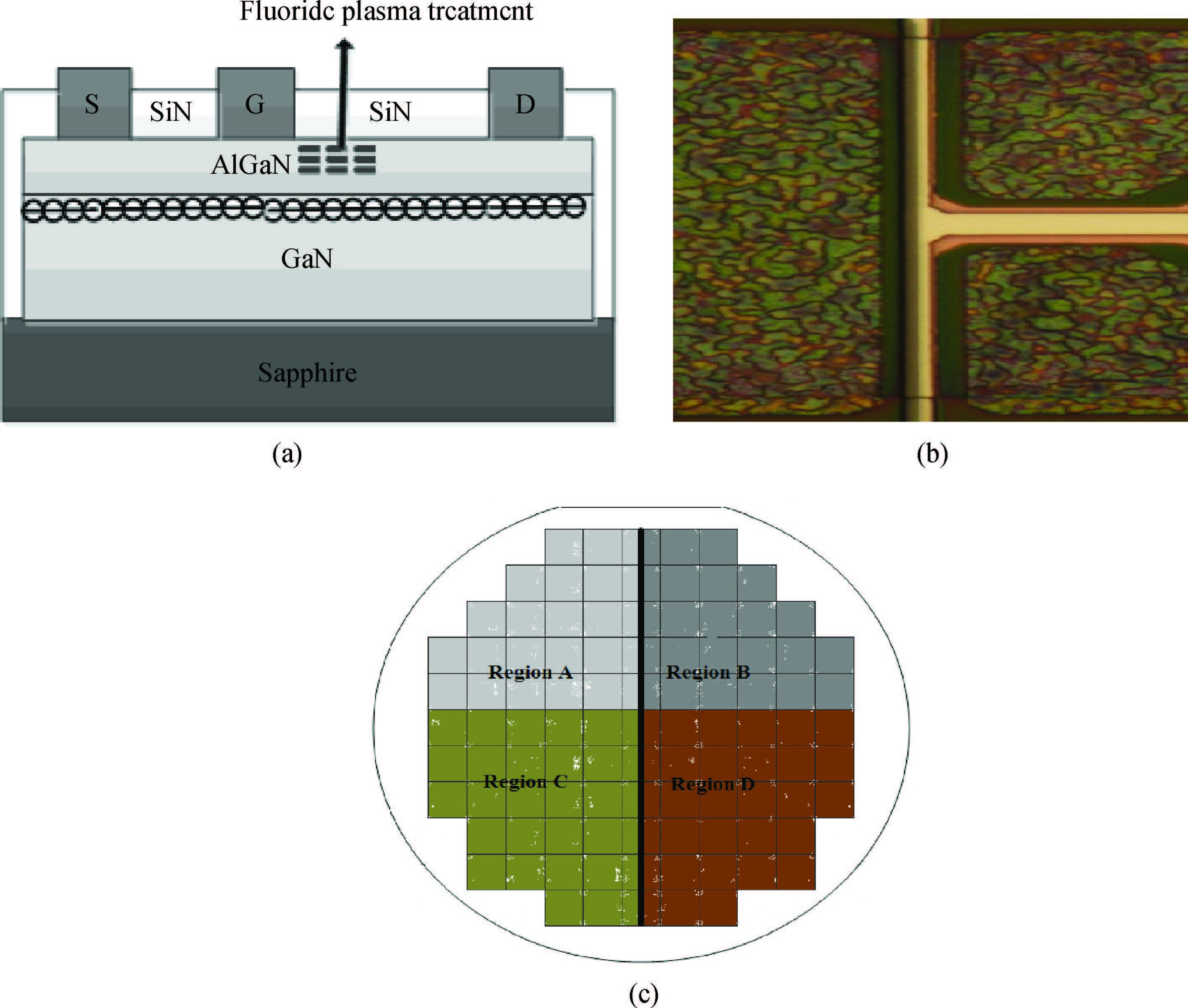
The AlGaN/GaN HEMT used in this paper was grown on a (0001) sapphire substrate in a metal organic chemical vapour deposition (MOCVD) system. The HEMT structure consists of a low-temperature GaN nucleation layer,a 1.8-μm-thick unintentionally doped GaN buffer layer and an 18-nm undoped AlGaN barrier layer. Room temperature Hall measurements of the structure yielded an electron sheet density of 1.22 × 1013cm-2 and an electron mobility of 1726 cm2(V⋅s). Figure 1 shows the schematic and microscopic image of LDD-HEMT under study in this paper.

Device mesa was formed by using Cl2/Ar plasma dry etching in a reactive ion etching (RIE) system,followed by the source/drain ohmic contact formation with Ti/Al/Ni/Au (30/180/55/45 nm) annealed at 850 ℃ for 30 s. In the same wafer,followed by the deposition of Ni/Au (30 nm/200 nm) by electron-beam evaporation,the four different areas of A,B,C,D were partitioned by stepper lithography machine shown as Figure 1(c). The region A was conventional AlGaN/GaN HEMT. F-based plasma treatment using CF4 capacitive coupled plasma (CCP) RIE apparatus was performed on the region B,C,D for 120 s with different RF power at 50,100 and 150 W,respectively. The flow rate of CF4 was 20 sccm at a pressure of 50 mT. Except for the F- plasma treatment process,the four different areas of the wafer had the same device processes. After SiN deposition of 60 nm on the device's surface by plasma-enhanced chemical vapor deposition (PECVD),the interconnection metal was fabricated. The gate length,gate width and source drain distance were 1,100 and 6 μm,respectively. The device electrical characteristics were measured by using the Keithley 4200 semiconductor parameter analyzer.
3. Results and analysis
In order to validate the feasibility of the LDD-HEMT,Silvaco software is used to simulate the off-state electric field distributions of LDD-HEMT and the conventional HEMT,respectively. Because of the crowding effect on the drain-side gate edge[17],there was a peak electric field at the gate edge. The peak electric field of LDD-HEMT was effectively reduced in the simulation results. The F- ions incorporated in the AlGaN layer of the LDD provide negatively fixed charges which can cause an upward bending of the conduction band,especially in the AlGaN barrier. It yields an additional barrier height[18],which can modulate the surface electric field and the 2DEG density,enable the redistribution of the E-field and reduce the peak field[19]. Therefore,LDD-HEMT shows lower 2DEG density and smaller output current.
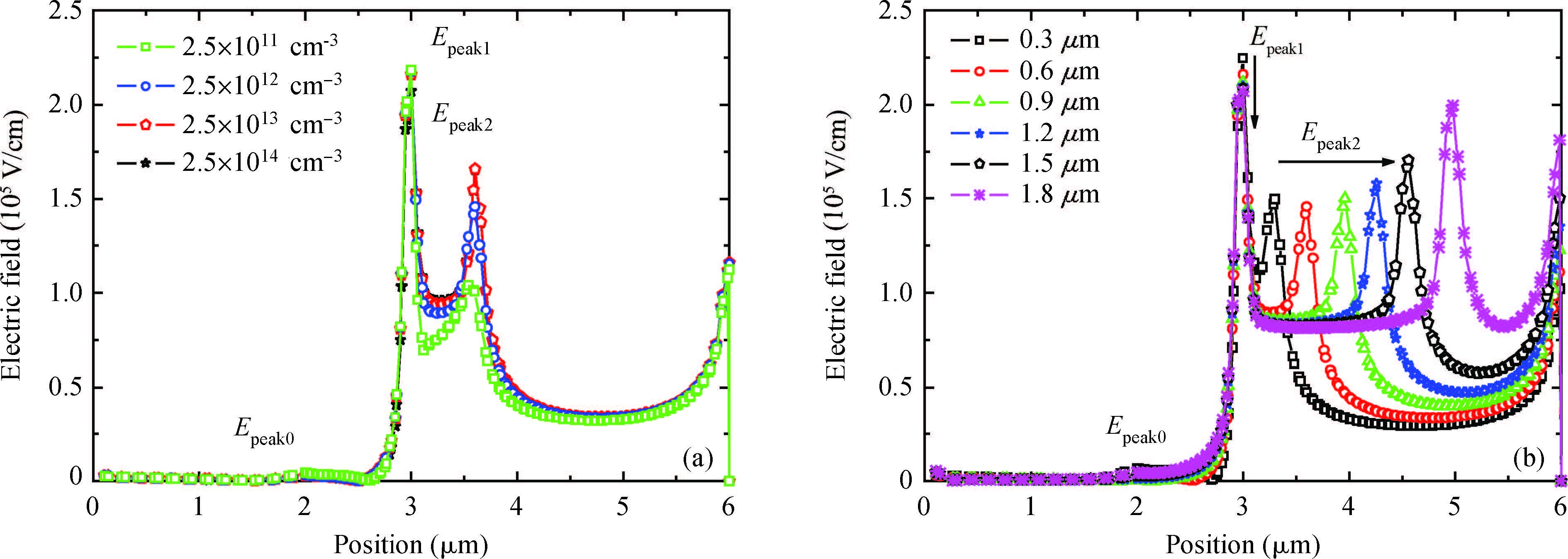
Different F- ions implantation dose and length were simulated by using Silvaco software,as shown in Figure 2. The source and drain side were respectively located at 0 and 6 μm in x-axis,while the gate located from 2 to 3 μm. Figure 2 shows that an additional electric field peak Epeak2 was introduced at the LDD edge. With the increase of F- ions implantation dose and length,Epeak2 increased gradually. Meanwhile,Epeak1,the peak electric field at the drain-side gate edge,decreased obviously. Especially in Figure 2(b),as F- ions implantation region was close to drain side,Epeak2 rightly had a movement toward drain side. With an area exposed to plasma treatment,the depletion region was expanded laterally rather than vertically in the barrier layer of the LDD device. The depletion region of the LDD HEMTs eased the concentrated electric field at the gate edge,and the uniform field distribution decreased the peak of the field at gate edge,therefore,the breakdown voltage of LDD-HEMT was improved.

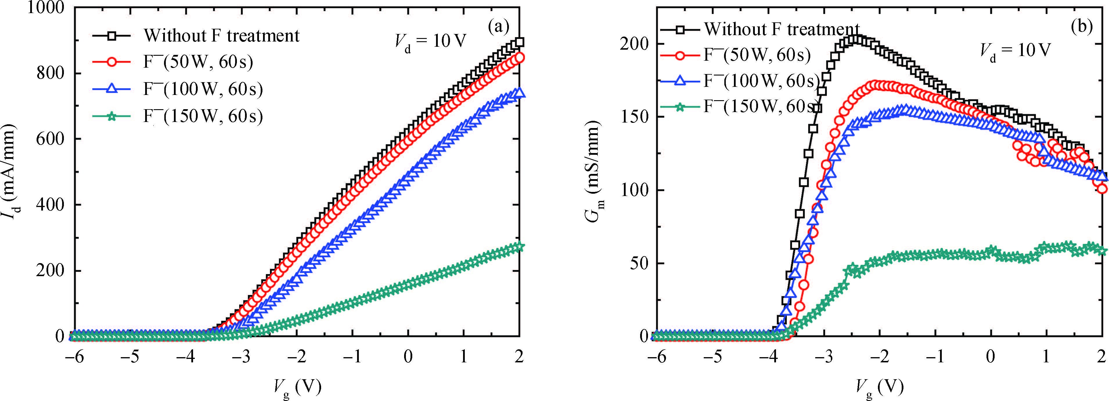
LDD-HEMTs with different F- plasma treatment power were investigated in experimentation. Figure 3 shows transfer characteristics of LDD-HEMT with different fluorine plasma treatment power. The LDD region was kept 0.6 μm in length.

The output current of the HEMTs without any fluorine plasma treatment reached about 900 mA. However,with the increase of the plasma treatment power in the LDD region,the output current of the HEMTs decreased. This phenomenon indicates that the 2DEG in the barrier layer has been partly depleted by the introduced F- ions. With the increased power,it also had an impact on the carrier mobility,so the transconductance decreased from 200 to 50 mS after 150 W fluorine plasma treatment,as shown in Figure 3(b). With the F- plasma treatment power increasing,the threshold voltage showed a slightly positive floating.
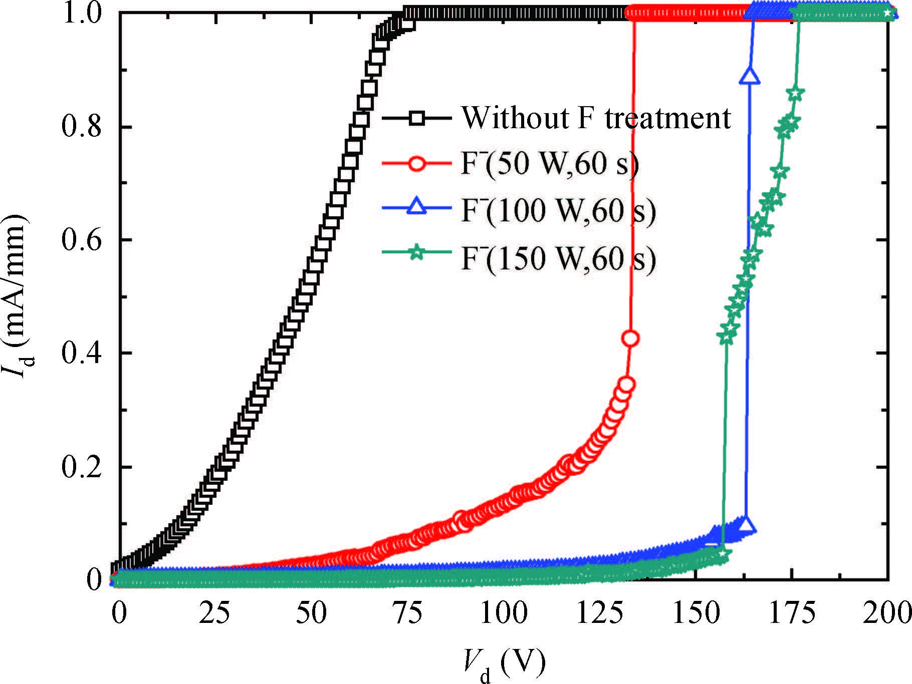
In this paper,the breakdown voltage is defined at drain current of 1 mA/mm,and it was measured at the off-state at VGS=-6 V. The breakdown characteristics with different F- plasma treatment power are shown in Figure 4. LDD region was still kept 0.6 μm in length. The breakdown voltage of the HEMT without any F- plasma treatment was 70 V,while those of LDD-HEMTs with 50,100 W F- plasma treatment power increased to 135,165 V,respectively. The main breakdown mechanism of the HEMTs was the avalanche breakdown,and the breakdown voltage was dominated by gate reverse leakage current[12],however,the gate reverse leakage current was impacted by the peak electric field at the gate edge,and the peak electric field were decreased in LDD-HEMTs. Increasing the plasma treatment power to 150 W,no further increase of the breakdown voltage was observed. The plasma damage on the surface of the AlGaN layer can be induced in high F- plasma treatment power,and the leakage current can be increased by trap-assisted tunnelling effect,so the effect of field modulation in LDD-HEMTs structure were reduced.

The breakdown characteristics of LDD-HEMT with different F- plasma treatment length and fixed F- plasma treatment power at 100 W are shown in Figure 5. It is clear that with LLDD increasing,the breakdown voltage increased obviously. The distance between the two peak fields increased with LLDD increasing,so that the distribution of electric field was dispersed,and the breakdown voltage can be improved with increased LLDD. Cho reported that the breakdown voltage of LDD HEMTs with gate-drain space of 10 μm enhanced from 1000 to 1400 V after F-based plasma treatment on the drain-side gate edge. A larger area was treated on the device with gate-drain space of 10 μm,so the breakdown voltage improved obviously.
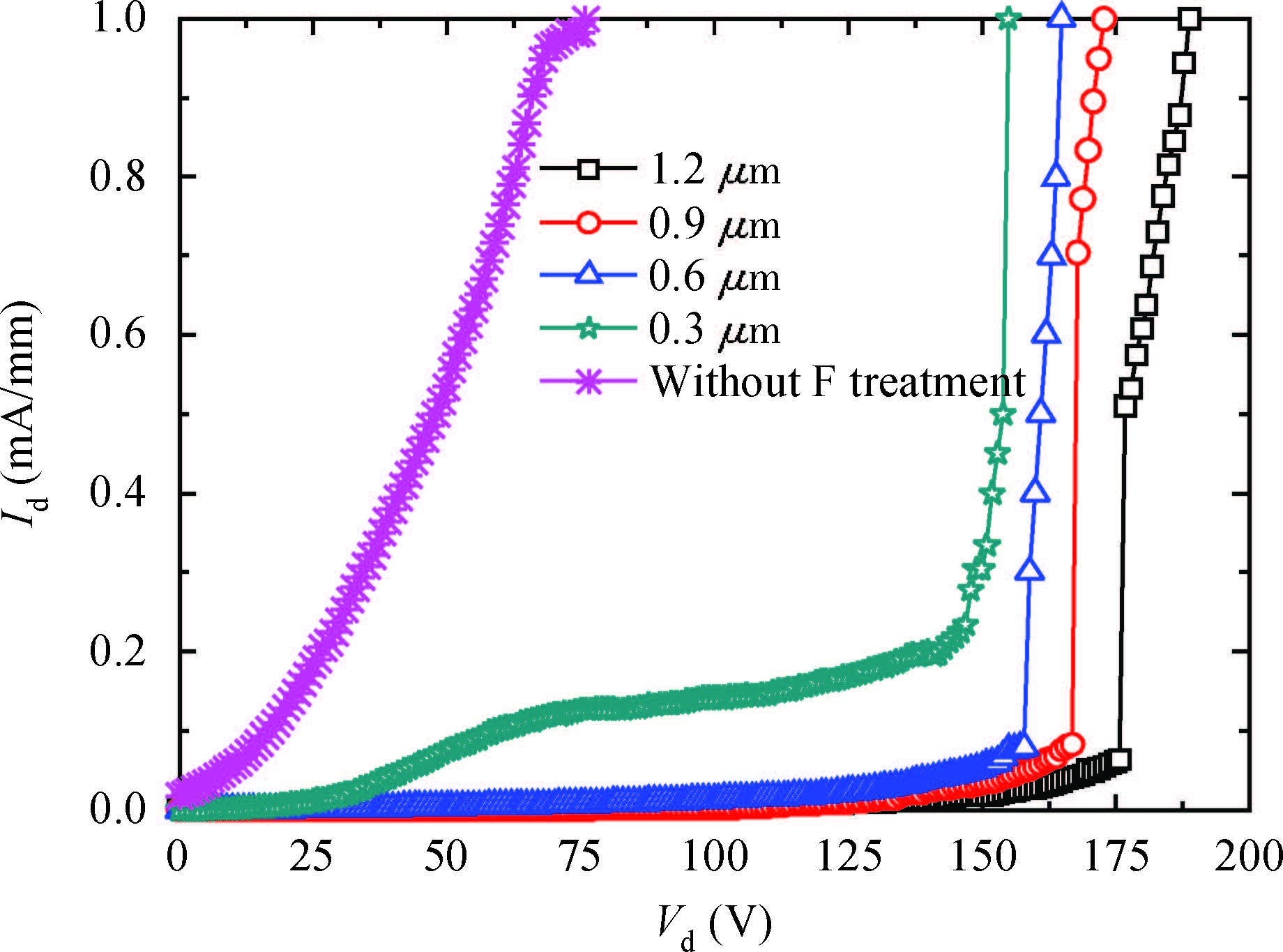
The Vth,Id,Gm and VB of different LDD-HEMTs with 0,0.3,0.6,0.9 and 1.2 μm LLDD were compared on the fixed F- plasma treatment power at 100W in this paper,as listed in Table 1. With the increase of LLDD,the saturation current and transconductance decreased significantly and the threshold voltages were almost the same. It can be explained by the reduction of 2DEG density and channel mobility with the increasing LLDD
| LLDD | Vth | Id (mA/mm) | Gm (mS/mm) | VB (V) |
| (μm) | (V) | (Vg = 2 V) | (Vd = 10 V) | |
| 0 | -3.2 | 950 | 200 | 75 |
| 0.3 | -2.7 | 870 | 190 | 155 |
| 0.6 | -2.5 | 440 | 140 | 165 |
| 0.9 | -2.5 | 390 | 68 | 173 |
| 1.2 | -2.5 | 358 | 55 | 188 |
 DownLoad:
CSV
| Show Table
DownLoad:
CSV
| Show Table
The shifted threshold voltages towards the negative direction were observed after annealing at 400 ℃ for 2 min in F implantation enhancement-mode AlGaN/GaN HEMTs[20],and the fluorine ions would diffuse in the AlGaN barrier until annealing temperature reached 600 ℃ . Therefore,the high temperature annealing effects on gate leakage current and breakdown characteristics of the LDD AlGaN/GaN HEMTs with different LLDD were investigated at 400 ℃ for 2 min in ambient N2,which are shown in Figures 6 and 7,respectively.
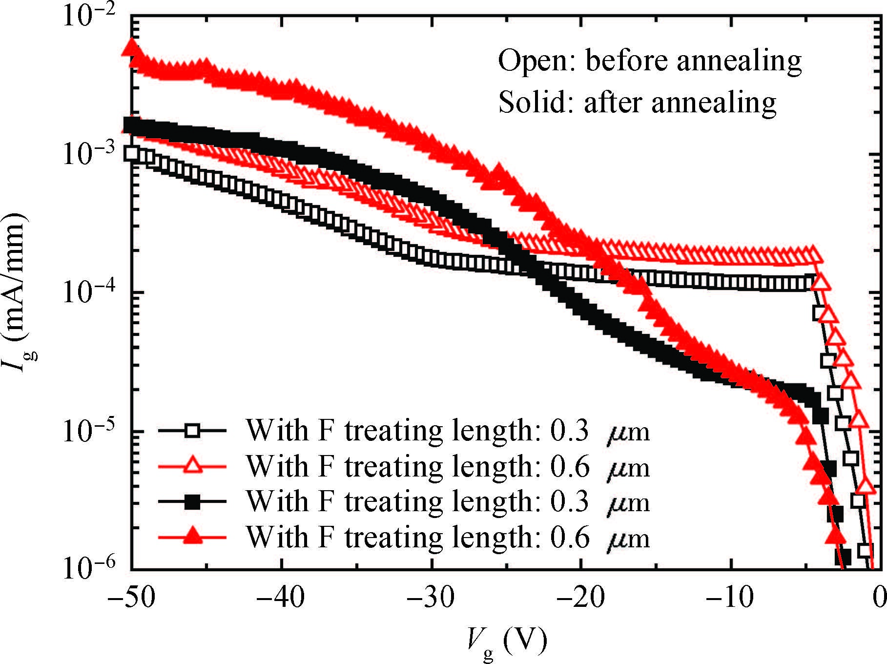
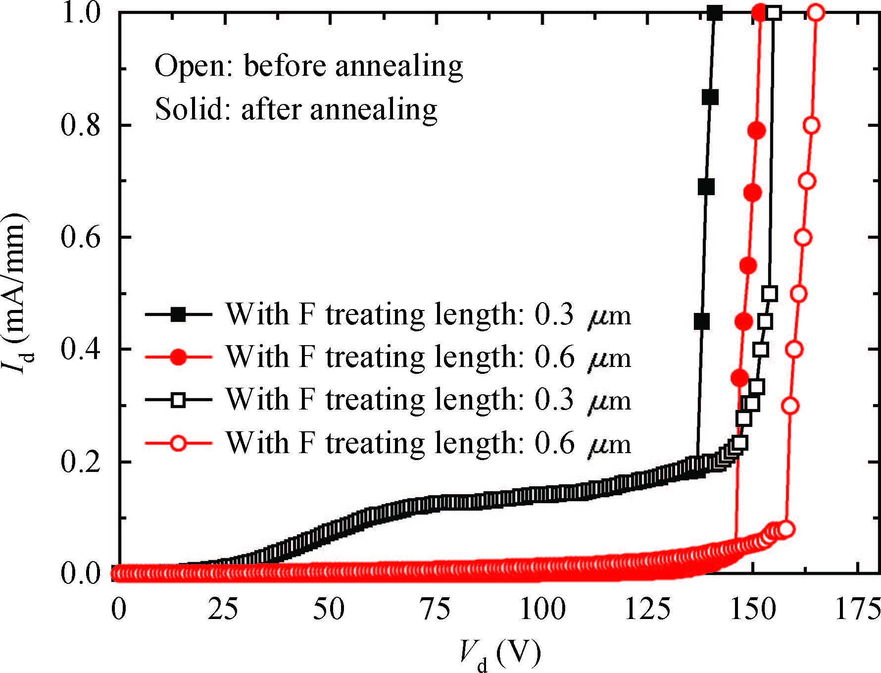
Fluoride plasma incorporated in the AlGaN layer creates states which are deep in the energy bandgap and effectively suppress the trapping-detrapping process on the surface[21]. Thus,the leakage current associated with shallow trap states is reduced by fluoride plasma treatment[20]. The F- ions implantation caused the leakage current to decrease by an order of magnitude compared with that of the conventional HEMT. It can be seen from Figure 6 that before annealing,the gate leakage currents were about 10-3 mA/mm at VGS=-50 V,and it has slightly increased after annealing. As the temperature increases,some of the electrons confined in the fluorine ions can be thermally excited,leading to a reduction in the density of the negatively-charged fluorine ions in the AlGaN layer[14]. The breakdown voltage of the LDD-HEMT with 0.6 μm LLDD was slightly reduced from 163 to 151 V after annealing. The depletion effect of F- ions and the increased barrier height of F- ions were weakened after annealing,so that the gate leakage current increases while the breakdown voltage decreases.
4. Conclusion
In this paper,investigations on LDD HEMTs with different F plasma treatment were implemented by simulation and experiments. As fluoride plasma implanted in the drain-side gate edge region,the reduction of peak electric field was verified by two-dimensional simulations using Silvaco simulation. The breakdown voltage enhancement and transfer characteristics reduction with the increase of LLDD were delivered. The breakdown voltage can be maximumly improved by 70% when the F- plasma treatment power was 100 W. Furthermore,annealing experiments were carried out at 400 ℃ for 2 min in ambient N2. The reverse gate leakage current of LDD-HEMT increased by less than one order of magnitude,and no severe reduction of breakdown voltages was observed.
 DownLoad: